

8XC196Kx, Jx, CA USER’S MANUAL
ANGND should be within about ± 50 mV of VSS. VREF should be well regulated and used only
for the A/D converter. The VREF supply can be between 4.5 and 5.5 V and must be able to source approximately 5 mA (see the datasheet for actual specifications). VREF should be approximately
the same voltage as VCC. VREF and VCC should power up at the same time, to avoid potential latchup conditions on VREF. Large negative current spikes on the ANGND pin relative to VSS may cause the analog circuitry to latch up. This is an additional reason to follow careful grounding practice.
The analog voltage reference (VREF) is the positive supply to which all A/D conversions are compared. It is also the supply to port 0 if the A/D converter is not being used. If high accuracy is not
required, VREF can be tied to VCC. If accuracy is important, VREF must be very stable. One way to accomplish this is through the use of a precision power supply or a separate voltage regulator
(usually an IC). These devices must be referenced to ANGND, not to VSS, to ensure that VREF tracks ANGND and not VSS.
11.6.1.4Using Mixed Analog and Digital Inputs
Port 0 may be used for both analog and digital input signals at the same time. However, reading the port may inject some noise into the analog circuitry. For this reason, make certain that an analog conversion is not in progress when the port is read. Refer to Chapter 6, “I/O Ports,” for information about using the port as digital inputs.
11.6.2 Understanding A/D Conversion Errors
The conversion result is the ratio of the input voltage to the reference voltage.
VIN – ANGND |
VIN – ANGND |
RESULT (8-bit) = 255 × ------------------------------------------ |
RESULT (10-bit) = 1023 × ------------------------------------------ |
VREF – ANGND |
VREF – ANGND |
This ratio produces a stair-stepped transfer function when the output code is plotted versus input voltage. The resulting digital codes can be taken as simple ratiometric information, or they provide information about absolute voltages or relative voltage changes on the inputs.
The more demanding the application, the more important it is to fully understand the converter’s operation. For simple applications, knowing the absolute error of the converter is sufficient. However, closing a servo-loop with analog inputs requires a detailed understanding of an A/D converter’s operation and errors.
11-14

ANALOG-TO-DIGITAL CONVERTER
In many applications, it is less critical to record the absolute accuracy of an input than it is to detect that a change has occurred. This approach is acceptable as long as the converter is monotonic and has no missing codes. That is, increasing input voltages produce adjacent, unique output codes that are also increasing. Decreasing input voltages produce adjacent, unique output codes that are also decreasing. In other words, there exists a unique input voltage range for each 10-bit output code that produces that code only, with a repeatability of typically ± 0.25 LSBs (1.5 mV).
The inherent errors in an analog-to-digital conversion process are quantizing error, zero-offset error, full-scale error, differential nonlinearity, and nonlinearity. All of these are transfer function errors related to the A/D converter. In addition, temperature coefficients, VCC rejection, samplehold feedthrough, multiplexer off-isolation, channel-to-channel matching, and random noise should be considered. Fortunately, one absolute error specification (listed in datasheets) describes the total of all deviations between the actual conversion process and an ideal converter. However, the various components of error are important in many applications.
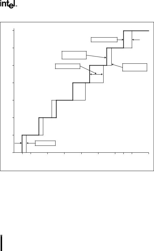
An unavoidable error results from the conversion of a continuous voltage to an integer digital representation. This error is called quantizing error and is always ± 0.5 LSB. Quantizing error is the only error seen in a perfect A/D converter, and is obviously present in actual converters. Figure 11-9 shows the transfer function for an ideal 3-bit A/D converter.
11-15

ANALOG-TO-DIGITAL CONVERTER
|
7 |
|
|
|
|
|
|
|
|
|
|
|
|
|
|
|
FULL SCALE ERROR |
|
|
|
|
|
6 |
|
|
|
|
|
|
|
|
|
|
|
|
|
IDEAL |
|
|
|
|
|
|
|
|
|
|
CHARACTERISTIC |
|
|
|
|
|
|
|
5 |
|
|
ABSOLUTE ERROR |
|
|
|
|
ACTUAL |
|
|
|
|
|
|
|
|
|
CHARACTERISTIC |
|
|
Ø |
4 |
|
|
|
|
|
|
|
|
|
OUTPUT |
|
|
|
|
|
|
|
|
|
|
Q CODE, |
3 |
|
|
|
|
|
|
|
|
|
|
|
|
|
|
|
|
|
|
|
|
|
2 |
|
|
|
|
|
|
|
|
|
|
1 |
|
|
|
|
|
|
|
|
|
|
|
|
ZERO OFFSET |
|
|
|
|
|
|
|
|
0 |
|
|
|
|
|
|
|
|
|
|
1/2 |
1 |
2 |
3 |
4 |
5 |
6 |
6 1/2 |
7 |
8 |
INPUT VOLTAGE (LSBs)
A0084-01
Figure 11-10. Actual and Ideal A/D Conversion Characteristics
The actual characteristic of a hypothetical 3-bit converter is not perfect. When the ideal characteristic is overlaid with the actual characteristic, the actual converter is seen to exhibit errors in the locations of the first and final code transitions and in code widths, as shown in Figure 11-10. The deviation of the first code transition from ideal is called zero-offset error, and the deviation of the final code transition from ideal is full-scale error. The deviation of a code width from ideal causes two types of errors: differential nonlinearity and nonlinearity. Differential nonlinearity is a measure of local code-width error, whereas nonlinearity is a measure of overall code-transition error.
11-17

8XC196Kx, Jx, CA USER’S MANUAL
Differential nonlinearity is the degree to which actual code widths differ from the ideal one-LSB width. It provides a measure of how much the input voltage may have changed in order to produce a one-count change in the conversion result. In the 10-bit converter, the code widths are ideally 5 mV (VREF / 1024). If such a converter is specified to have a maximum differential nonlinearity of 2 LSBs (10 mV), then the maximum code width will be no greater than 10 mV larger than ideal, or 15 mV.
Because the A/D converter has no missing codes, the minimum code width will always be greater than –1 (negative one). The differential nonlinearity error on a particular code width is compensated for by other code widths in the transfer function, such that 1024 unique steps occur. The actual code widths in this converter typically vary from 2.5 mV to 7.5 mV.
Nonlinearity is the worst-case deviation of code transitions from the corresponding code transitions of the ideal characteristic. Nonlinearity describes the extent to which differential nonlinearities can add up to produce an overall maximum departure from a linear characteristic. If the differential nonlinearity errors are too large, it is possible for an A/D converter to miss codes or to exhibit non-monotonic behavior. Neither behavior is desirable in a closed-loop system. A converter has no missing codes if there exists for each output code a unique input voltage range that produces that code only. A converter is monotonic if every subsequent code change represents an input voltage change in the same direction.
Differential nonlinearity and nonlinearity are quantified by measuring the terminal-based linearity errors. A terminal-based characteristic results when an actual characteristic is translated and scaled to eliminate zero-offset and full-scale error, as shown in Figure 11-11. The terminal-based characteristic is similar to the actual characteristic that would result if zero-offset and full-scale error were externally trimmed away. In practice, this is done by using input circuits that include gain and offset trimming. In addition, VREF could also be closely regulated and trimmed within the specified range to affect full-scale error.
Other factors that affect a real A/D converter system include temperature drift, failure to completely reject unwanted signals, multiplexer channel dissimilarities, and random noise. Fortunately, these effects are small. Temperature drift is the rate at which typical specifications change with a change in temperature. These changes are reflected in the temperature coefficients. Unwanted signals come from three main sources: noise on VCC, input signal changes on the channel being converted (after the sample window has closed), and signals applied to channels not selected by the multiplexer. The effects of these unwanted signals are specified as Vcc rejection, off-isolation, and feedthrough, respectively. Finally, multiplexer on-channel resistances differ slightly from one channel to the next, which causes channel-to-channel matching errors and repeatability errors. Differences in DC leakage current from one channel to another and random noise in general contribute to repeatability errors.
11-18

ANALOG-TO-DIGITAL CONVERTER
|
7 |
|
|
|
|
|
|
|
|
|
|
|
|
|
|
IDEAL FULL-SCALE CODE |
|
|
|
|
|
|
|
|
|
|
TRANSITION |
|
|
|
|
|
|
6 |
|
|
|
|
|
|
|
|
|
|
|
|
|
IDEAL STRAIGHT LINE |
|
|
|
|
|
|
|
|
|
|
TRANSFER FUNCTION |
|
|
|
|
ACTUAL |
|
|
|
|
|
|
|
|
|
FULL-SCALE CODE |
|
|
|
|
|
|
|
|
|
|
|
TRANSITION |
|
|
5 |
|
|
DIFFERENTIAL |
|
|
|
|
|
|
|
|
|
|
|
|
|
TERMINAL BASED |
|
||
|
|
|
|
NON-LINEARITY |
|
|
|
|
||
|
|
|
|
(POSITIVE) |
|
|
|
CHARACTERISTIC |
|
|
|
|
|
|
|
|
|
|
(corrected for zero-offset |
||
|
|
|
|
IDEAL |
|
|
|
and full-scale error) |
|
|
|
|
|
|
|
|
|
|
|
|
|
Ø |
4 |
|
CODE WIDTH |
|
|
|
|
|
|
|
OUTPUT |
|
|
|
|
|
|
|
|
ACTUAL |
|
|
|
|
|
|
|
|
CHARACTERISTIC |
|
||
|
|
|
|
|
|
|
|
|
|
|
Q CODE, |
3 |
|
|
|
|
|
|
|
|
|
|
|
|
|
|
|
|
|
|
|
|
|
|
|
|
NON-LINEARITY |
|
|
|
|
|
|
|
2 |
|
|
|
|
|
|
|
|
|
|
|
|
|
DIFFERENTIAL |
|
|
|
|
|
|
|
|
|
|
NON-LINEARITY (NEGATIVE) |
|
|
|
|
||
|
1 |
|
|
|
|
|
|
|
|
|
|
|
|
|
IDEAL CODE WIDTH |
|
|
|
|
|
|
|
|
|
ACTUAL FIRST TRANSITION |
|
|
|
|
|
|
|
|
|
|
IDEAL FIRST TRANSITION |
|
|
|
|
|
|
|
|
0 |
|
|
|
|
|
|
|
|
|
|
1/2 |
1 |
2 |
3 |
4 |
5 |
6 |
6 1/2 |
7 |
8 |
INPUT VOLTAGE (LSBs)
A0085-01
Figure 11-11. Terminal-based A/D Conversion Characteristic
11-19

12
CAN Serial
Communications
Controller

<PageNum>-22