Of crucial importance in many systems are time-related functions. This may manifest itself in the measurement of duration, event counting or control of an external physical event for known periods. An example of the former would be the time between pulses generated by the teeth on a flywheel to measure engine speed for a tachometer.
Where time is of the essence these functions are often best implemented by using hardware counters to time events. In this chapter we will look at the various timer modules which are available to the mid-range PIC family. After completion you should:
•Know how a Watchdog timer improves the robustness of a MCU-based system and how to use the integral PIC device.
•Be able to use the basic 8-bit Timer 0 module as both a counter and timer.
•Understand the function of the 16-bit Timer 1 module and its interaction with the Capture/Compare/PWM (CCP) modules.
•Be able to use the 8-bit Timer 2 module together with the CCP modules to generate a pulse-width modulated output.
Many MCU-based systems are hosted in an electrically hostile environment with noise induced outside both through logic lines and the power supply. Our example of an auto tachometer is typical of this situation, with induction from the high-voltage ignition sparks and alternator sourced ripple in the battery supply. No matter what precautions in shielding and filtering are taken, it is inevitable that on occasion the MCU will jump out of its proper location in Program memory and ‘run amok’ with potentially serious consequences on the controlled system.1 In some cases this is little more serious than requiring a manual reset.2 However, this is not possible in many situations; for example, in a pacemaker implanted in the patient’s body!
One solution to this problem is to use a counter/oscillator which resets the processor when it overflows. If the software is arranged to clear this counter on a regular basis so that overflow never occurs then the
1The same can happen due to software bugs.
2As in a Window’s PC.
362 The Quintessential PIC Microcontroller
MCU never resets. If something happens and the MCU jumps out of its normal loop then the counter will overflow and the MCU will be reset to its starting point. This counter circuit is given the name Watchdog timer.3
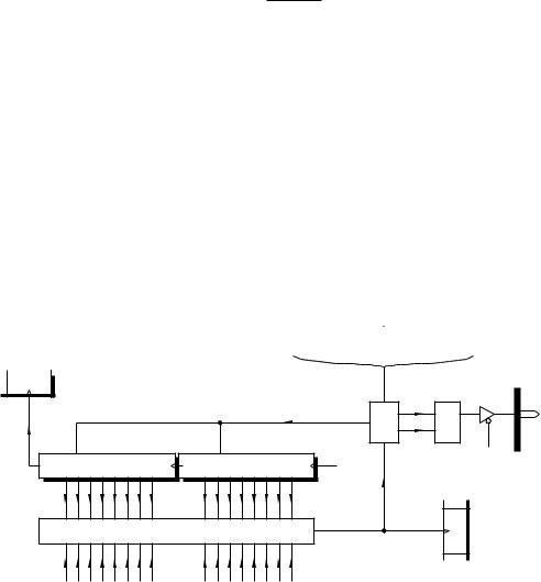
clrwdt
STATUS
File 03h
Reset PIC
reset up-Power
S 4
TO
R
Postscaler
÷128
÷64
÷32
÷16
÷8
÷4
÷2
÷1
110
101
100
011
010
001
111
000
R
CNTR8 C+ R
G
wdt fuse
Watchdog timer oscillator/counter 18 ms (nominal)
0
PS0
1
PS1
2
PS2
1 3 OPTION_REG
File 81h
Fig. 13.1 The integral PIC Watchdog timer.
Rather than rely on external Watchdog timers, all PIC MCUs, even the early 12-bit PIC16C5XX family, have an integral module as illustrated in Fig. 13.1. A built-in oscillator separate from the processor clock runs continually if the Watchdog timer is enabled, with a nominal period of 18 ms. The integral capacitor/resistor timing network is not tightly specified and as a consequence the period will vary with device process, temperature and supply voltage from a minimum of 7 ms (lowest temperature −40◦C,
highest VDD 6 V) up to a maximum of 33 ms (highest temperature +85◦C, lowest VDD 2 V) – see Fig. 15.8 on page 448.
The Watchdog oscillator is followed by an 8-bit Watchdog postscaler counter. This prescaler be set to give Watchdog counter overflow timeout periods going up in powers of two up to nominally 18 × 128 ≈ 2.3 s
– 0.9 s minimum, 4.2 s maximum. The actual value is selected by the programmer using the PS[2:0] (Pre/Post Scaler rate Select) bits in the Option register (OPTION_REG) – see Fig. 13.2. The Watchdog postscaler and counter are both cleared with the clrwdt (CLeaR WatchDoG Timer) instruction and issuing this at regular intervals is the mechanism whereby the programmer prevents time-out.
3Other approaches typically are based on a retriggerable monostable.
The Watchdog timer postscaler is a shared resource with Timer 0 (see Fig. 13.3) and cannot be used for both functions. The PSA (Pre/Post Scaler Assignment) bit is used to assign this resource either to the Watchdog timer or to Timer 0. On Reset the postscaler is assigned to the Watchdog timer and time-out is set to ÷128.
Even with this default assignment the programmer must enable the latter by setting the WDTE configuration fuse, as described in Fig. 10.5 on page 261; for example:
__config _HS_OSC & _WDT_ON & _PWRTE_OFF & _CP_OFF
or the equivalent that is appropriate to your C compiler; for instance, in the CCS compiler:
#fuses HS, WDT, NOPUT, NOPROTECT
If the Watchdog timer overflows it clears the TO (Time Out) bit in STATUS[4] – see Fig. 4.5 on page 89. This bit is set by the clrwdt or sleep instruction and on Power-on reset. clrwdt also sets the PD status bit. TO is cleared after Watchdog time-out has occurred; as listed in Table 10.3 on page 266. It is not changed if the PIC is manually reset. TO is a read-only bit and therefore cannot be altered by the programmer other than by using clrwdt or by putting the MCU in its Sleep state.
Unless the PIC is sleeping a Watchdog reset will force execution to begin at the normal Reset vector 000h. In some circumstances the programmer may want to distinguish between the two sources of reset. For example, assume that a system is counting cans of beans moving along a conveyer belt in the manner shown in Fig. 13.4, keeping a tally in a file register called BEAN_COUNT. On Power-on this tally is to be zeroed. If due to a glitch the PIC’s Watchdog times out and the PIC resets, then this tally should be left unchanged. To do this we can use code to check the state of TO and take the appropriate action; for instance:
364 The Quintessential PIC Microcontroller
__config
_WDT_ON
;
Enable the Watchdog timer
org
000h
;
The Reset vector
MAIN btfss
STATUS,NOT_TO ;
Was this a Watchdog reset?
clrf
BEAN_COUNT
;
IF not THEN zero tally
; more initializing code
clrwdt
;
Set NOT_TO and reset Watchdog
Resetting initializes the Watchdog timer and zeros the postscaler so it’s not necessary to issue an extra clrwdt as we have done above. However, the initializing process will add to the time it takes to get into the normal main code and the normal loop clrwdt, thus an extra clrwdt at the end of any initializing code is useful insurance.
In the 12-bit PIC family the Watchdog time-out was the only way short of a Manual reset to awaken a device in the Sleep state. The sleep instruction resets the Watchdog and postscaler counters to give a full timeout period when entering the Sleep state. As the Watchdog oscillator is stand-alone it continues to run while the PIC is asleep. After the ordained period a Watchdog reset occurs and the PIC resumes execution with the instruction following sleep. If necessary the programmer can determine that the time-out occurred during the Sleep state by examining the TO bit.
The Watchdog awaken mechanism is not so important for the midand high-range PIC families. These can be awakened by an external interrupt, and where applicable the Timer 1 and Analog modules, both of which have the option of a self-standing clock oscillator. Where the watchdog is enabled and used in the Sleep mode the designer should be aware that the typical current consumption4 rises from typically 1.5 µA (24 µA maximum) to 10.5 µA (42 µA maximum). Where long-term battery operation is required (for example, see SAQ 12.6 on page 360) this presents serious problems. Running the processor continually at the lower frequency of 32.768 kHz with the Watchdog disabled takes typically 52 µA (105 µA maximum) in comparison.
The original 12-bit PIC16C5XX family features a basic 8-bit counter/- prescaler which was called a Real-Time Clock/Counter. Although this term was still used in the early 14-bit PIC16CXXX data sheets, the introduction of additional timers lead to the more consistent term Timer 0 (TMR0). However, the term RTCC is still to be found as a relic in older textbooks and software. For example, the CCS C compiler sets the Timer 0 clock source to external low-going edge with a prescale value of 4 by calling setup_counters(rtcc_ext_l_to_h, rtcc_div_4);.
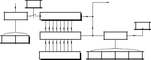
From Fig. 13.3 we see that Timer 0 comprises a primary 8-bit counter located at File 1 in tandem with an optional 8-bit prescaler counter. This gives eight selectable clock rates into the primary counter as selected by the three PS[2:0] bits in OPTION_REG. This Timer 0 prescaler is actually
4The PIC16C74 with VDD = 4 V, −40◦C to +85◦C.
File 1
TMR0
Timer 0
Overflow
2
T0IF
Fosc /4
Synch
INTCONh
File 0B
1
0
13. Time is of the Essence 365
Prescaler
0
Fosc
/4
RA4
÷256
÷128
÷64
÷32
÷16
÷8
÷4
÷2
101
100
011
1
T0CKI
111
110
010
001
000
0
PS0
1
PS1
2
PS2
4
T0SE
5
T0CS
PSA3 OPTION_REG
File 81h
Fig. 13.3 Simplified equivalent circuit for Timer 0.
the same circuit as the Watchdog’s postscaler5 and PSA in OPTION_REG[3] must be set to 0 to assign the prescaler to Timer 0.
The prescaler is assigned to the Watchdog timer by default on Poweron/Manual reset and in this situation the primary counter is either clocked by the internal cycle clock Fosc at a rate XTAL/4 or from an outside source via the Timer 0 Clock Input RA4/T0CKI pin. The Timer 0 Clock Select
T0SC bit at OPTION_REG[5] is used to select the internal/external mode. When clocked from outside, the active edge is set using the Timer 0 Set Edge T0SE bit at OPTION_REG[4].
In order to synchronize the outside clock to the internal Timer 0 primary counter, a 2-stage shift register is used at the latter’s clock input.
This causes a 2 × Fosc/4 delay; 1 µs with an 8 MHz crystal. Where the primary counter is directly connected to the internal clock, this will cause
a 2-count delay before anything happens after a datum is written into Timer 0 at File 1. This synchronization is such that Timer 0 may be read from or written to in the normal way without interfering with any possible count action.
When the primary counter overflows (11111111 → 00000000) the Timer 0 Interrupt Flag T0IF is set. This event can be sensed by polling
INTCON[2] or if the Timer 0 Interrupt Enable mask bit T0IE in INTCON[5] is set an interrupt will automatically be generated – see Fig. 7.4 on page 178.
An external clock signal going directly into the primary counter should
be high for at least 2Tosc +20 ns and low for at least the same time. Thus for a 8 MHz crystal, Thigh should be 270 ns and the same for Tlow; a max-
5The PIC18CXXX family use separate scalers for the Watchdog timer and Timer 0.
366 The Quintessential PIC Microcontroller
imum frequency of 1.8 MHz. When the prescaler is used this minimum
total period of 4Tosc + 40 ns can be divided by the prescaler ratio. The input waveform is subject only to a minimum 10 ns pulse width. Thus
with a ÷256 setting, a nominally 50 MHz signal at T0CKI will be counted. When assigned to Timer 0 the prescaler is not readable, so the timer is not strictly a 16-bit counter. Reading Timer 0 does not a ect the prescaler but any instruction writing to it (eg. clrf 1, movwf 1) will both clear the
prescaler and the clock synchronizer.
As the prescaler is assigned to the Watchdog on Power on/Manual reset it can be subsequently changed over by clearing PSA. However, it is possible that this change-over could cause a Watchdog reset even if it is disabled. Microchip therefore recommend that the change-over be preceded by a clrwdt instruction; for example:
clrwdt
;
Clears postscaler and wdt
bsf
STATUS,RP0
;
Change-over to Bank0
movlw
b’11110001’
;
External clock on low-going edge
movwf
OPTION_REG
;
1:4 Timer0 prescaler
bcf
STATUS,RP0
;
Back to Bank1
The code shows the prescaler divides clock input by four from the T0CKI pin, and incrementing on the \ . It is also possible to change the prescaler over from Timer 0 to the Watchdog timer ‘on the fly’. In the same manner the clrwdt should be executed before altering OPTION_REG to avoid a spurious Watchdog reset.
Timer 0 is mainly used either to count external events or to determine the period between external events. it can also be used to time software toggling port pins for precisely known durations, without tying up the processor in time-wasting delay routines.
VDD
To packing machine
RB1
Noise
buffer
T0CKI/RA4
Sensor
Fig. 13.4 Counting cans of beans on a conveyer belt.
13. Time is of the Essence 367
We will illustrate the usage of Timer 0 as an event counter and stop clock with two examples. The first is to tally cans of baked beans travelling along a conveyer belt, as shown in Fig. 13.4. Each 24 cans passing the sensor is to generate a pulse to a packing machine, so that the box can be replaced by a new empty container. This pulse need only be a few microseconds in duration. A double-byte count is also to be kept of the number of boxes packed since the last Power-up/Manual reset. This will be uploaded to the central plant computer at the end of the shift for inventory control.
Our first consideration is the setup and initialization code. The code shown below begins by checking the TO flag at the Reset vector. If zero then the bulk of the initialization code is omitted as reset was due to a Watchdog time-out. If this was not the case then port pin RA4/T0CKI is set up as an input and RB1 set up as an output to activate the packing machine.
include
"p16F84.inc"
__config
_WDT_ON
; Enable Watchdog
cblock 20h _work:1, _status:1 COUNT:2
endc
org
0
;
Reset vector
btfss
STATUS,NOT_TO ;
Ckeck if a Watchdog reset
goto
MAIN_LOOP
;
IF yes THEN no initialization
goto
MAIN
;
ELSE a fresh start
org
4
;
Interrupt vector
goto
ISR
;
Foreground program
MAIN
bsf
PORTB,1
;
Idle state of the Packing pulse
bsf
STATUS,RP0
;
Change to Bank1
bsf
TRISA,4
;
Make sure that T0CK1 is I/P
bcf
TRISB,1
;
& RB1/Packing machine an O/P
movlw
b’00101111’
;
Timer source external -ve edge
movwf
OPTION_REG
;
prescaler assigned to wdt
bcf
STATUS,RP0
;
Back to Bank0
bsf
INTCON,T0IE
;
Enable Timer0 interrupt
movlw
-d’24’
;
Initialize TMR0 to -24 (E8h)
movwf
TMR0
clrf
COUNT+1
;
Clear the 2-byte score count
clrf
COUNT
bsf
INTCON,GIE
;
Enable all interrupts
; The
background program which
amongst other things
MAIN_LOOP
clrwdt
;
Regularily resets the wdt
...
.....
;
More background code
368 The Quintessential PIC Microcontroller
The Option register, also in Bank 1, is set up to assign the prescaler to the Watchdog and extend its time-out period by ×128. The Timer 0 counter is set to be clocked from T0CKI on a negative-going edge. Finally, back in Bank 0 Timer 0 itself is set to E8h (i.e. −24 decimal) so that 24 can pulses will cause it to overflow and cause an interrupt. Both INTCON flags T0IE and GIE are then set to enable the interrupt.
The main background program commences with a clrwdt instruction. Provided that the background endless loop is no longer than 7 × 128 = 0.8961 s, the minimum Watchdog period, then time-out will not occur.
With the initialization code in situ all that remains is to implement the Interrupt Service Routine (ISR) that will be automaticlly entered after each batch of 24 cans. When this occurs, Timer 0 will set T0IF and the PIC will jump to the Interrupt vector at 004h. In our initialization code we have placed a goto ISR at this point and so named the routine in Program 13.1.
Program 13.1 The bean counter Interrupt Service Routine.
The ISR itself is sandwiched between the normal context switching wrapper described in Program 7.2 on page 183. The core simply implements the following task list in no particular order:
•Toggle RB1 to signal the packing machine.
•Reset Timer 0 to −24.
•Increment the double-byte score count.
•Reset the Timer 0 Interrupt flag T0IE.
In Program 13.1 T0IE is tested on entry and if not set the ISR is exited. If there are other sources of interrupt then the switch would be to another part of the ISR, as shown in the listing on page 179.
For an alternative approach using hardware interrupts see Program 7.2 on page 183.
Our second example illustrates the use of Timer 0 as a clock to measure time between events. The events in question are R-points peaks in the ECG waveform illustrated in Fig. 7.1 on page 172. Here a peak detector interrupts the MCU, which keeps a 2-byte count from a 10 kHz external oscillator. In this manner the period between events can be determined on each event in increments of 100 µs, which we call here ji es. For our example we will modify the specification to eliminate this oscillator and use Timer 0 to keep a 1 ms 2-byte Ji y tally.
For this task we need to use the main PIC oscillator as the clock source together with the prescaler that so that Timer 0 overflows once per millisecond (103 µs). If we choose a 4.096 MHz crystal we have:
Time-out = 4.0964 × 256 × prescale ratio
which gives a required prescale ratio of 1:4.
With these requirements in mind we have for our initialization background software:
org
0
; Reset vector
goto
MAIN
; Background program
org
4
; Interrupt vector
goto
ISR
; Foreground program
MAIN clrwdt
; Change prescaler to Timer0
bsf
STATUS,RP0
; Change to bank1
movlw
b’00000001’
; INT on -ve edge, internal clock
movwf
OPTION_REG
; prescale div4
bcf
STATUS,RP0
; Back to Bank0
bsf
INTCON,T0IE
; Enable Timer0 interrupt
bsf
INTCON,INTE
; Enable exteral interrupt
clrf
NEW
; Zero the New flag
bsf
INTCON,GIE
; Enable all interrupts
As well as enabling the Timer 0 interrupt, INTE is set to enable hardware interrupts from the INT pin which is going to signal an ECG peak. Neither
370 The Quintessential PIC Microcontroller
Program 13.2 Measuring the ECG waveform period to a resolution of 1 ms.
the double-byte Ji y count nor Timer 0 need be cleared as the first reading of the series will always be erroneous – as the patient’s heartbeat is not synchronized to the PIC reset! However, file register NEW which is set to non zero each time an ECG peak is detected is cleared.
The core of the ISR shown in Program 13.2 implements the following task list when an interrupt is received:
1.IF Timer 0 interrupt.
• Increment 2-byte Ji y count.
13. Time is of the Essence 371
•Reset Timer 0 interrupt flag.
•Return from interrupt.
2.ELSE a hardware interrupt form peak picker.
•Copy ji y count into general-purpose file registers.
•Zero Timer 0.
•Set New flag.
•Reset hardware interrupt flag.
•Return from interrupt.
Both bytes in COUNT:COUNT+1 are copied into the two data file registers DATUM:DATUM+1 when a hardware interrupt is received and the Ji y count/Timer 0 is then zeroed ready for the next event. When the background program polls file register NEW and finds a non-zero datum then it knows that a fresh count is ready for collection. It then, for instance, could send it to a serial EEPROM as in Example 12.3 on page 351 or down a serial link to a PC for subsequent processing and display.
Most midand high-range PICs have at least two additional timer/counters and associated circuitry with the following properties.
Timer 1
This 16-bit counter has its own dedicated oscillator and programmable prescaler. Its state can be sampled by an external event and it can control the state of a pin when it reaches a pedefined value.
Timer 2
This 8-bit counter has both programmable pre and postscaler facilities. Its count length can be set by the programmer and it may be used to generate a pulse-width modulated output with no on-going software overhead.
Capture/Compare/PWM
Both timers can be used in conjunction with additional logic called Capture/Compare/Pulse Width Modulation (CCP) to implement the Timer 1 sample instant (Capture), the Timer 1 roll-over value (Compare) and the automatic PWM generation from Timer 2.
Timer 1 comprises a primary 16-bit counter implemented as a pair of file registers at File 0Eh for the low byte TMR1L and File 0Fh for the high byte TMR1H. The Timer 1 CONtrol register TMR1CON at File 10h configures Timer 1 as shown in Fig. 13.5.
Timer 1 has the option (T1OSCEN in T1CON[3] = 1) of using a separate oscillator from the main PIC oscillator. This avoids having to pick the main crystal to suit the timer, as we did in our Timer 0 bean counter example. Some older PIC devices, such as the PIC16C74A, require the RC0/T1CKI pin to be set as input for the oscillator to function. Newer devices, such as the PIC16C74B, do not need this configuration. The Timer 1 oscillator has a maximum frequency of 200 kHz but is typically used with
372 The Quintessential PIC Microcontroller
File 0Ch
CCP
File 10h
special event trigger
0
PIR1
0
T1CON
TMR1IF
TMR1ON
2
T1CON
Overflow
Timer 1
T1SYNC
File 0Fh
File 0Eh
1R
C
1R
C1
Synchronize
TMR1H
TMR1L
F
Oscillator
osc
<200kHz
F
/4
T1OS0/T1CKI
osc
0
Prescale
1 ÷1, ÷2, ÷4, ÷8
T1OS1
EN
3
1
5
4
T1OSCEN
TMR1CS
T1CKPS1
T1CKPS0
T1CON
T1CON
T1CON
Fig. 13.5 Functional equivalent circuit for Timer 1
a 32.768 kHz watch crystal. Where this is the case, Timer 1 will overflow in 2 seconds with a prescale ratio of 1:1 (T1CKPS[1:0] = 00) and a maximum of 16 s for a prescale ratio of 1:8 (T1CKPS[1:0] = 11). When overflow takes place, the Timer 1 Interrupt Flag in the Peripheral Interrupt Register 1 PIR1[0] is set. If the corresponding TMR1IE mask in the Peripheral Interrupt Enable 1 register PIE1[0] then an interrupt will occur. All interrupt flags and mask bits for Timer 1, Timer 2 and their related CCP modules are located in PIR1, PIR2, PIE1 and PIE2 as shown in Fig 14.10(b) on page 408. To enable all these interrupts the PEIE (PEripheral Interrupt Enable) bit in INTCON[6] must be set as well as the overall GIE global mask bit in INTCON[7]. The latter should be 0 if the only action required is to awaken the PIC from its Sleep state, but PEIE must still be set.
The Timer 1 oscillator adds approximately 20 µa current drain which is a consideration that is especially important if it is intended to use Timer 1 to awaken the processor. Where power consumption is at a premium then a low-power external oscillator should be considered. In this situation with T1OSCEN = 0 the external oscillator should drive the T1CKI pin. Limitations on the upper frequency of such an input are similar to that discussed for Timer 0. Alternatively the internal PIC clock can be used if TMR1CS is zeroed (the reset condition), but of course this stops when the processor is in its Sleep state.
Output from the programmable prescaler is by default synchronized to the internal clock giving a 2-cycle delay. However, unlike Timer 0 this synchronization shift register can be bypassed with T1SYNC set to 1.
13. Time is of the Essence 373
This needs to be done to allow Timer 1 to operate in the Sleep mode as Fosc is disabled in this situation. Apart from this case T1SYNC should be 0 as the lack of synchronization can lead to an unpredictable outcome if data is written into the two Timer 1 primary registers. If the Timer 1 state is to be updated, then the count should be stopped by clearing TMR1ON during this process; for instance:
movlw
80h
bcf
T1CON,TMR1ON
; Stop the timer
movwf
TMR1H
;
Set Timer1 to 8000
clrf
TMR1L
bsf
T1CON,TMR1ON
;
Restart the timer
Altering the state of Timer 1 will always clear the prescale counter. Timer 1 can be read at any time whatever the state of T1SYNCH. How-
ever, as only one byte can be read at a time6 it is possible that the timer may have overflowed from lower to higher byte in between the two reads; for example:
; Assume Timer1 is at state
80FFh
movf
TMR1L,w
; Read low byte = FFh
movwf
TEMPL
; Store away
; «« Timer 1 now increments
to state 8100h »»
movf
TMR1H,w
; Get
high byte = 81h
movwf
TEMPH
; Store away
erroneously reads the state as 81FFh instead of 80FFh. This is even more likely to occur if another peripheral device interrupts between reads. A predictable reading can be obtained by either stopping Timer 1 before taking the readings or by reading the high byte first and then checking after the low byte has been read that the high byte has not changed.
The T1CON register is zeroed on Power-on and Manual reset – see Appendix B. This means that Timer 1 defaults to o with an internal clock source and prescale value of 1:1.
For our example assume that we have a low-power temperature logger that is to read the sensor and transmit its value back to base once every 15 minutes. It is proposed that Timer 1 be used to action this process and that the Timer 1 oscillator with a 32.768 kHz watch crystal is to give the timebase.
Timer 1 has a maximum overflow rate of 16 seconds, but if set to 4 seconds we will have a whole number of 15 interrupts per second. If we keep a Ji y count then a total of 15 × 15 = 225 will give 15 minutes. Thus our set up and main skeleton software would be something like that shown in Program 13.3. Here Timer 1 is set up to use the external
6In the PIC18CXXX family reading one of the bytes of Timer 1/3 automatically makes a copy of the other byte in a temporary register, e ectively giving a single 16-bit time sample.
374 The Quintessential PIC Microcontroller
Program 13.3 Generating a 15 minute data logger timebase.
oscillator with a prescale ratio of 2:1, giving our 4 s ji y. In addition, both TMR1IE, PEIE and GIE mask bits are set to enable the interrupt on Timer 1 overflow.
The ISR simply adds one onto the Ji y count. This is tested for 225 in the background program after sleep and if equal it is zeroed, the temperature taken and transmitted to base.
Timer 1 can be reset to zero by any Compare/Compare/PWM CCP module. Some PIC devices have two CCP modules sharing the same timer, such as the PIC16C74, and in such cases the second module CCP2 is virtually identical to CCP1 and can share the same timer. With this in mind we will look just at CCP1 for convenience, pointing out any di erences at the relevant point. All CCP operations require Timer 1 to be configured in its synchronous mode; that is SYNCH = 0.
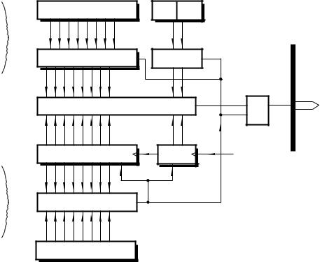
Each CCP module has an associated control register. For CCP1 this is CCP1CON at File 1Dh in which the lower four bits CCP1M[3:0] set the module mode. A setting of 0000, the reset value, disables the CCP module, resets the CCP output latch and clears the Capture mode prescaler. Modes 1000 – 1011 listed in Fig. 13.6 give four Compare modes. Here an equality comparator detects when the 16-bit Timer 1 datum equals the setting in the 16-bit CCPR1H:L (CCP Register 1) at File 15:16h respectively. When an equality match occurs the CCP1IF interrupt flag in PIR1[2] will be set and this can cause an interrupt if the corresponding CCP1IE mask bit in PIE1[2] is set.
Besides setting CCP1IF and depending on the setting of the CCP1M[3:0] mode bits, one of four actions are possible on Timer 1 matching CCPR1:
0000
CCP1 off
3
2
1
0
CCP1CON
1000
CCP1 pin high on match
CCP1M3
CCP1M2
CCP1M1
CCP1M0
File 17h
File 0Ch
1001
CCP1 pin low on match
1010
CCP1 pin unchanged on match
0
1011
Reset Timer 1 on match
TMR1IF
PIR1
CCP latch
RC2
R
O/P
CCP1
Overflow
1R TMR1H
1RTMR1L
logic
S
C1
File 0Fh
File 0Eh
TRISC[2]
Timer 1
PIR1
Comparator
Match
2 CCP1IF
=
CCP Register 1
CCPR1H
CCPR1L
File 16h
File 15h
Fig. 13.6 The CCP1 module set to Compare mode.
376 The Quintessential PIC Microcontroller
1000:
Pin RC2/CCP1 is forced high.
1001:
Pin RC2/CCP1 is forced low.
1010:
Pin RC2/CCP1 unchanged, but CCP1IF still set.
1011:
Timer 1 is cleared and with CCP2 only7 an analog module conversion is initialized by setting GO/DONE – see Fig. 14.8 on page 404.
Where RC2/CPP1 or RC1/CCP2 are to be used as CCP outputs then the appropriate TRISC bit(s) should be cleared to set the pin direction to output. There is no way to directly reset or set the CCP latch other than zeroing the CCPCON register which resets the latch and disables the CCP module. In this case the state of the RC2/CCP1 pin will be that of PORTC[2] until the module is set to an appropriate mode, in which case the pin will reflect the state specified above when the match occurs.
As an example consider that we wish to set up Timer 1 as configured in the last example to generate an interrupt each 10 seconds. To do this we need set the timer to time-out after 16 s (prescale ratio 8:1) and then shorten the cycle. This is implemented by loading the CCPR1 register with the fraction 1016 −1, which translates to 9FFFh. Whenever Timer 1 reaches this value it will automatically be reset on the next clock input (that would have normally incremented the timer to A000h) and an interrupt will occur if the CCP1IE mask bit (and global PEIE and GIE masks) are set.
Initialization code for this is:
movlw
9Fh
; Set up CCPR1 to 9FFFh
movwf
CCPR1H
movlw
FFh
movwf
CCPR1L
movlw
b’00001011’
; CCP Compare mode 1011
movwf
CCP1CON
movlw
b’00111011’
; Timer1 on (1), external clock (1)
movwf
T1CON
; Synched (0), oscillator (1) 8:1 (111)
bsf
STATUS,RP0
; Change to Bank 1
bsf
PIE1,CCP1IE
; Enable CCP1 interrupts
bcf
STATUS,RP0
; Change back to Bank 0
bsf
INTCON,PEIE
; Enable Timer/CCP interrupts
bsf
INTCON,GIE
; Enable all interrupts
The PIC will then automatically be interrupted every ten seconds.
As CCP1 is not changed by Compare mode 1011 this pin can be used as a normal Port C input/output independently of the CCP1 module.
Where there are two CCP modules they can work in tandem using di erent modes, but the timebase will be common – see Example 13.3.
7This is the only functional di erence between CCP1 and CCP2.
13. Time is of the Essence 377
Modes 0100 – 0111 configure the appropriate CCP module to capture the state of Timer 1 when an ‘event’ occurs at the appropriate CCP pin. We can see from Fig. 13.7 that an event can be a falling or rising edge on the RC2/CCP1 pin or every 4th or 16th rising edge according to the CCP1M[3:0] mode bits. This Event prescaler is cleared when the mode bits are set to 0000.
Once a defined event has taken place the 16-bit state of Timer 1 is parallel loaded into the CCP register 1 and CCP1IF set. The processor can then subsequently read this frozen value – that is the time. If Timer 1 is reset after each capture then the sampled datum is the time since the last event. Alternatively, as Timer 1 continues to increment, its captured value can be subtracted from the previous reading to give the di erence. As the mode may be altered on the fly, the time between rising and falling edge on CCP1 can be measured by toggling CCP1M[0] between captures. This may cause the CCP1IF flag to be set. To prevent false interrupts, CCP1IE should be cleared before the change-over and CCP1IF after the change-over. Alternatively, the CCP1 module can be used to capture the rising edge and CCP2 the falling edge – see Example 13.3. There is no room for the CCP2IF and the associated interrupt mask CCP2IE mask bit in PIR1/PIE1. Instead bit 0 of PIR2/PIE2 are pressed into service and in many mid-range processors is the only occupant of these registers.
As our example, consider that we wish to measure the period of our ECG signal with the peak detector connected to pin CCP1. If we assume Timer 1 is clocked by its own 32.768 kHz watch crystal, our set up code is something like this:
File
PIR1 h0C
CCP1IF
2
TMR2IF
1
TMR1IF
0
CCP1CON
File 17h
3
2
1
0
0100
Every falling edge
CCP1M3 CCP1M2 CCP1M1 CCP1M0
0101
Every rising edge
0110
Every 4th rising edge
CCP1 Control register
0111
Every 16th rising edge
Prescaler
CCP Register 1
÷1, ÷4, ÷16
File 16h
File 15h
C CCPR1H
C CCPR1L
Timer 1
CCP1
TMR1H
TMR1L
File 0Fh
File 0Eh
Fig. 13.7 Capturing the time of an event.
378 The Quintessential PIC Microcontroller
movlw
b’00001011’
; Timer on, external clock, synched
movwf
T1CON
; Oscillator enabled, PS ratio 1:1
movlw
b’00000100’
; Capture mode, event = falling edge
movwf
CCP1CON
clrf
NEW
; Zero NEW flag
bsf
STATUS,RP0
; To Bank1
bsf
PIE1,CCP1IE
; Enable the CCP1 interrupt
bcf
STATUS,RP0
; Back to Bank0
bsf
INTCON,PEIE
; Enable Timer/CCP interrupts
bsf
INTCON,GIE
; Global interrupts enabled
The ISR simply reads the contents of the CCP register and stores it away in two temporary locations, setting the file register NEW to indicate to background program that a new time datum exists. Timer 1 is then reset ready for the next event.
With a crystal of 32.768 kHz the time resolution of the captured datum is 30.5 µs with our 1:1 prescale setting. Timer 1 will overflow in 2 s, which is su cient to record a heart rate of 30 beats per minute.
Program 13.4 Capturing the instant of time an ECG R-point occurs.
A more robust software system would also enable the Timer 1 overflow interrupt. if this occurs it indicates that the subsequent captured data will be invalid – although time-outs can be counted and thus extend the validity of the captured time. However, in our system it is more likely to be used to set o an alarm!
Timer 2 is an 8-bit counter which has both pre and postscalers. Unlike the two previous timers, output is not taken from the counter chain but from the Timer 2 Comparator. This compares the state of Timer 2 with that in the Period Register PR2. On equality an output pulse is generated which resets Timer 2 at the next clock pulse. This reset signal also sets the Timer 2 Interrupt Flag TMR2IF in PIR1[1]. The number of equality events to set TMR2IF and optionally create an interrupt, is a function of the postscaler. Any integer number between 1 and 16 events can be set up using the TOUTPS[3:0] (Timer 2 OUTput Post Scaler) in the Timer 2 CONtrol register at T2CON[5:2]. T2CON at File 12h also controls the prescaler, giving four divide ratios for the internal clock, and can also be used to disable the timer. The reset state of T2CON is all zeros, disabling the timer and giving a pre/post scaler ratio of 1:1.
The advantage of this architecture is that time-out can be fine tuned by setting the Period Register to an appropriate value, independently of a CCP module. The period until TMR2IF is set is given as:
4/Fosc × Prescale × (PR2 + 1) × Postscale
For our example, consider the need for an interrupt 100 times per second to scan a 7-segment display (see Program 11.8 on page 302) and that the main crystal is 4 MHz. Choosing a prescale ratio of 4:1 gives a clocking period for Timer 2 of 4 µs. If the Period Register is set to 249 then the Timer 2 comparator output period is 250 × 4 = 1 ms. Thus setting
Fosc /4
T2CON
2
Timer 2 output
TMR2ON
(to SCI
port
baud clock)
File 11h
Prescaler
Timer 2
R
÷1, ÷4, ÷16
File 0Ch
TMR2
1
TMR2IF
TMR2 Comparator
Postscaler
PIR1
=
1
0
÷1 to ÷16
T2CKS1
T2CKS0
T2CON
File 12h
PR2
Period Register
5
4
3
2
TOUTPS3 TOUTPS2 TOUTPS1 TOUTPS0
File 92h
T2CON
Fig. 13.8 A simplified equivalent circuit for Timer 2.
380 The Quintessential PIC Microcontroller
the postscaler to 1:10 (1001) will give a 10 ms (100 Hz) interrupt rate. By varying the postscaler from 1 to 16 (TOUTPS[3:0] = 0000 to 1111) respectively we can have an interrupt rate from 1 to 16 ms. For fine adjustments a unit change in PR2 alters the rate by 4 × postscaler × µs.
Set up code for this example is:
movlw
b’01001101’
; Postscale 1:10 (1001), Timer2 on (1)
movwf
T2CON
; Prescale 1:4 (01)
bsf
STATUS,RP0
; Change
to Bank1
movlw
d’249’
; Set up
period register to 249
movwf
PR2
bsf
PIE1,TMR2IE
; Enable
Timer2 interrupts
bcf
STATUS,RP0
; Change
back to Bank0
bsf
INTCON,PEIE
; Enable
all Timer/CCP interrupts
bsf
INTCON,GIE
; Global
enable
One of the more common applications of MCU-based systems is the control of power circuits, such as heating, lighting and electric motor speed control. One approach to this problem would be to use a digital to analog converter, such as that discussed in Fig. 12.16 on page 328, driving a power amplifier. Linear control is expensive and ine cient due to the large current:voltage products that must be handled by the power amplifier. A rather more e cient and more cost e ective approach rapidly switches the load on and o at a reasonably fast rate. A power switch, such as a thyristor, dissipates relatively little power, as when the switch is o no current flows and when the switch is on the voltage across the switch is low – ideally zero.
An example of such a waveform is shown in Fig. 13.9. The average amplitude is simply A × N%, where N is the duty cycle percentage of the repeat period. If we vary N from 0 to 100% then the average power will vary in a like fashion – all without the benefit of analog circuitry. This digital to analog conversion technique is known as pulse width modulation (PWM).
The thermal or mechanical inertia of most high-power loads is such that even with a relatively low repetition rate (typically no lower than 100 Hz) the ‘bumps’ will be smoothed. Low switching rates are more efficient, as each switching action dissipates energy. If PWM is used for more conventional digital to analog conversion, such as for audio, then a
Duty
cycle
Period
A
Fig. 13.9 Pulse width modulation.
13. Time is of the Essence 381
low-pass filter may be utilized to reduce the high-frequency harmonics. In such cases a sampling rate of at least ten times the maximum analog signal should be used to space out the harmonics (see Fig. 14.3 on page 396) and reduce the necessary filtering burden.
It is relatively easy to generate a PWM waveform solely in software by simply counting and setting a port pin when the count rolls over to zero and resetting the pin when it equals the datum representing the duty cycle. Thus if the duty cycle datum was 9Fh and the period count was module-256 (00–FFh) then the average power would be 62.5% (58 ).
CCP modules have a PWM mode in conjunction with Timer 2, as shown in Fig. 13.10. Here Timer 2 runs with a period determined by the main crystal, prescaler and Period Register 2 as previously described. When the Timer 2 comparator causes the count to reset, it also sets the PWM latch. This gives the PWM repeat period.
A second CCP equality comparator matches the 10-bit duty cycle number which is set up by the program in CCPR1L and the two bits DC1B[1:0] (Duty Cycle 1 Bits) in CCP1CON[5:4]. Taken together this gives a 10-bit duty-cycle datum DC1B[9:0]. This datum is loaded into the CCPR1H and a slave 2-bit latch each time Timer 2 rolls over. CCPR1H is not directly writable to in this mode. Thus we have the following sequence of operations repeated indefinitely:
CCPR1L
5
4
CCP1CON
DC1B1 DC1B0
File 17h
Duty cycle
registers
Slave
CCPR1H
C
Latch
C
PWM latch
RC2/CCP1
10-bit PWM Comparator
=
R
S
Timer 2
Prescaler
Timer 2
1RC1
1R
C1
Fosc /4
T2CKPS[1:0]
Period
8-bit TMR2 Comparator =
registers
CCP1M[3:0] = 11XX
Period Register
Fig. 13.10 Timer 2 and the PWM CCP mode.
382 The Quintessential PIC Microcontroller
1.Timer 2 increments.
2.When Timer 2:Prescaler equals DC1B[9:0] the PWM latch resets and pin CCP1 goes low.
3. The
next clock pulse after Timer 2 reaches the datum in PR2 it is reset.
The
PWM latch is set, CCP1 goes high and the 10-bit slave duty cycle regis-
ter/latch us updated. 4. Goto item 1.
From the above description we see that:
•The PWM period is set by the Timer 2/PR2 time-out.
•The duty cycle is set by the 10-bit datum in CCPR1L:CCP1CON[5:4].
•The duty cycle datum can be glitchlessly changed by the software at any time by updating the slave registers and will take e ect in the PWM period following this update.
•The RC2/CCP1 pin direction should be set to output.
Where the Timer 2 prescale is set to 1:1 the lower two bits used on the timer side are the quadrature clock phases described in Fig. 4.4 on page 87. This gives a period resolution equal to the crystal period. In all cases the datum in CCPR1L must be smaller than that in PR2, otherwise the PWM latch will never reset!
If PR2 is FFh then the resolution of the system is a full ten bits. Smaller values of Timer 2 period data will reduce this resolution. For example, if PR2 = 3Fh then the resolution is reduced to eight bits – six in PR2 and two in the prescaler.
For our example let us assume a crystal frequency of 20 MHz, a prescale ratio of 1:16 and a PR2 value of FFh. In this case the PWM frequency is 204 × 161 ×256 = 1.22 kHz. A prescale ratio of 1:1 would increase the period frequency to 19.53 kHz. Reducing the value in PR2 would also increase the repetition frequency. The programmer need only place the duty cycle datum in CCPR1L and CCP1CON[5:4] (the latter can be left at its reset value of zero if the datum is to be treated as 8-bit) and a PWM signal will automatically be generated with no software overhead. Set up code for this instance would be:
bsf
STATUS,RP0
; Change to Bank0
movlw
FFh
; Set up Timer2 Period register
movwf
PR2
; to FFh
bcf
TRISC,2
; Make RC2/CCP1 an output
bcf
STATUS,RP0
; Change back to Bank1
movlw
b’00001100’
; CCP1 module PCM mode (1100)
movwf
CCP1CON
movlw
b’00000110’
; Timer2 prescale 16:1 (10),
movwf
T2CON
; Timer2 on (1)
The Timer 2 postscaler does not a ect the PWM generation but still sets the TMR2IF in the normal way. The CCP1IF is not altered in this mode.
13. Time is of the Essence 383
If a second CCP module is used, an extra PWM output at pin RC1/CCP2 is available with a separate duty cycle but an identical period, as Timer 2 is a shared resource.
Examples
Example 13.1
Show how you could use Timer 0 to generate a PWM version of a digital byte in file register DATUM using pin RA0 as the output. Assuming an 8 MHz crystal, calculate the PWM duration.
Solution
Timer 0 will give a time-out related to a number loaded into the timer at the beginning of the period. If we load in the the 2’s complement of the byte (the negative value) then the duration will be proportional to this value – the larger it is the longer the timer has to count before overflowing. Conversely loading in the value of DATUM will give a time-out duration inversely proportional to the value. By alternately loading the 2’s complement of DATUM and making the pin high followed by DATUM itself making the pin low will give us a total period approximately the same as a total Timer 0 time-out as if counting through all 256 states.
The coding of Program 13.5 sets up Timer 0 to count 2 MHz internal clock cycles with no prescale. Thus the total PWM rate is 2562 or 7.8125 KHz. When Timer 0 overflows it generates an interrupt. The ISR checks the state of PORTAA[0] and if 0 changes its state and then calculates the 2’s complement of the data byte (invert plus one). However, there is a 2-cycle delay in Timer 0 responding when its state is changed due to the clock synchronizer circuit and so another two is added to compensate for this extra delay. If the port pin was already 1 then it is zeroed and the datum itself plus the compensatory two is written into Timer 0.
Adding the compensation will cause problems at either extremes of the mark:space ratio. Why is this so and what action could you take to ameliorate it?
Example 13.2
A certain tachometer is to register engine speed in the range 0–12,000 rpm (revolutions per second). The engine generates one pulse per revolution and it is intended that a PIC16C74 be used to count the number of pulses each second and calculate the equivalent rpm. Using two of the three available timers can you design a suitable hardware-software configuration?
Solution
384 The Quintessential PIC Microcontroller
Program 13.5 Pulse-Width Modulation using Timer 0.
A speed of 12,000 rpm translates to a maximum pulse count of 200 rps (revolutions per second). Thus we propose to use Timer 0 as the pulse counter driven from pin T0CKI with no prescaler.
Timer 1 in conjunction with CCP1 set to a Compare mode will give a 1-second time-out if it uses its own oscillator and a 32.768 kHz watch crystal together with a count spanning 0000–7FFFh. However, to simplify the mathematical relationship rpm = rps × 60 it is proposed to shorten the timebase by the factor 6064 to implement the equivalent relationship
rps×60 × 64. The final ×64 can easily be implemented by either shifting
64
left six times (>>6) or more e ciently placing the rps count as the high byte of the double-byte rpm datum and shifting right twice; i.e.:
rpm = (rps × 256)> >2
This is considerably more e cient that using a 1 second timebase and multiplying by 60.
One possible solution is shown in Program 13.6. Here the initialization code implements the following task list:
• Set Timer 0 to count \ events at T0CKI.
•Set CCP1 to Compare mode 1011 to reset Timer 1 on equality.
•Enable an interrupt from this event.
•Set up the CCPR1H:L to set the timebase to 6064 s.
The ISR itself simply copies the rps reading from Timer 0, zeroing it and then converts the reading to rpm as described above. After the two shift right operation >>2, the top two bits of RPM are cleared to remove erroneous carry-ins. The resulting 14-bit datum in RPM:RPM+1 is the required outcome which can then perhaps be used by the background program to activate the display or maybe transmit the data to a computer over a serial link.
Example 13.3
A PIC16C74 is to be used to measure the duration of an event. This duration is the time a signal is high, as shown in Fig. 13.11. You an assume that the main crystal is 8 MHz and the duration of the event is guaranteed to be no more than 100 ms.
Solution
One way of tacking this problem is to feed the signal shown in the diagram into both pins RC1 and RC2 in parallel. Using one CCP module to capture the rising edge and the other to capture the falling edge gives the duration as the di erence in the two captured values. In Program 13.7 Timer 1 is zeroed on a rising edge and thus the second captured Timer 1 state is our duration. If we use a prescale ratio of 1:4 and the internal clock
Fig. 13.11 An event manifesting itself as a pulse duration.
then we have as our counting rate 500 kHz; i.e. the system resolution is 2 µs. The overall maximum duration that can be measured in this way is 216 × 2 = 131, 077µs which is large enough not to overflow.
The ISR in Program 13.7 simply tests each CCP interrupt flag in turn and goes to the appropriate routine. If CCP1 has signalled a / event
then the timer is zeroed to restart the count. Timer 1 has been configured to increment at a 500 kHz rate and when the next \ occurs the CCP2 module captures the state of this timebase and places it in the 16-bit CCPR2 register. The ISR then copies it into the two file registers TIME:TIME+1 and this is the period in 2 µs ticks.
Actually resetting Timer 1 on the first event introduces some inaccuracy into the process as the clearing event takes some time. In our application this is of little consequence but it may cause some problems in shorter high-resolution situations. In this case Timer 1 can be left to run continually and the two captured 16-bit data subtracted to give the required di erence at relative leisure.
Self-assessment questions
13.1Using Timer 1 and CCP1, design a system to generate a continuous square wave with a total period of 20 ms from RC2/CCP1. You may assume that the main crystal is 8 MHz. Hint: Remember that the state of the CCP pin will only change when a match occurs so the Compare mode will have to be changed on the fly each 10 ms.
13.2The echo sounding hardware shown in Fig. 7.6 on page 195 uses an external 1.72 kHz oscillator to interrupt the PIC once per 5.813 ms, that is once every time sound travels 1 cm through air. Assuming that a 20 MHz PIC is used, show how Timer 2 could be used to generate this interrupt rate to an accuracy better than 0.1%.
13.3The PIC family has only one hardware input, namely INT/RB0. Suggest
some way to use Timer 0 to simulate another hardware interrupt with pin T0CKI/RA4.
13.4As part of a software implementation of an asynchronous serial channel running at 300 baud a delay of 3.3˙ ms is to be generated. Assuming that a 8 MHz PIC16F84 is the host processor, show how you could use a timer to generate an interrupt each baud period. Extend your routine to enable baud rates up to 19,200 in doubling geometric progression.
13.5Show how you would use Timer 1 with its separate integral oscillator with a 32.768 kHz watch crystal, to keep the central heating real time clock array HOURS:MINUTES:SECONDS of Example 7.4 on page 191 up to date.
13.6The CCS C compiler has integral functions dealing with the timers and CCP modules. For example, Timer 1 can be written to using set_timer1(datum); and read from using get_timer1();. The function setup_timer_1(mode); is used to initialize the timer. Similarily setup_ccp1(mode); initializes the CCP1CON register. Mode
values for Timer 1 and the CCP Compare configuration are:
Where separate modes can be separated by the operator |.
Show how you would code your solution to SAQ 13.5 in C. In CCS C a function can be turned into a CCP1 interrupt service routine by preceeding it by the directive #INT_CPP1 – see Program 14.9 on page 427 for details. You an also assume that the reserved variable CCP_1 represents the 16-bit CCPR1H:L register.


 reset up-Power


 ÷1, ÷2, ÷4, ÷8