

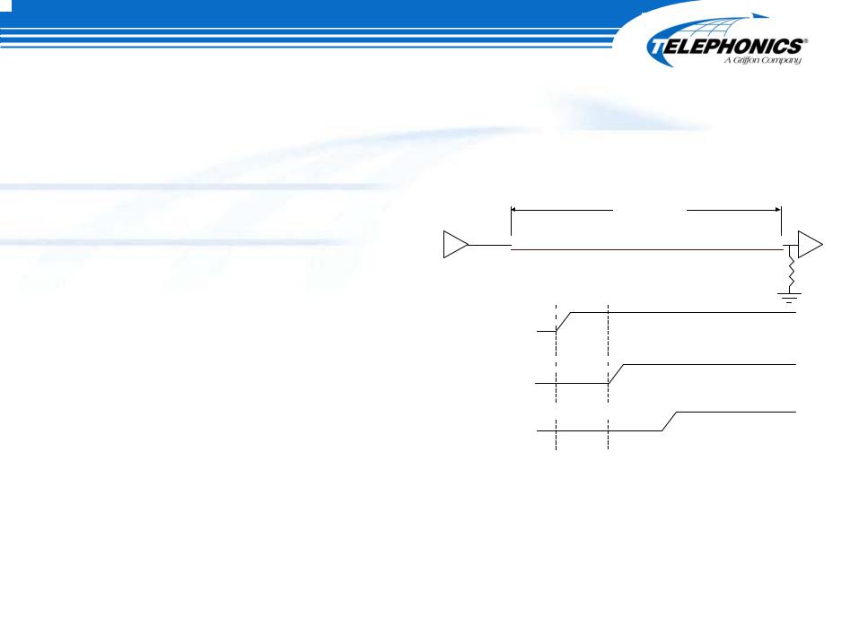
Destination Terminations
♦Driving waveform propagates at full intensity over trace
♦Reflections dampened
by terminating resistors(s)
♦Received voltage is equal to transmitting voltage (ignoring losses)
♦Increased peak current demands on driver
Delay = T |
|
Zo=50 Ω |
C |
A B
50 Ω
1 


 A
A 
0
1 


 B
B 


0
1 


 C
C 


0
0 |
T |
2T |
♦More applicable to daisy-chained receivers (first incident switching)
♦Thevenin termination reduces steady-state drive current
Revision 4 |
Copyright Telephonics 2002-2005 |
59 |
|
“Intentional” Mismatch Exampleple
♦
♦
♦
Five selectable sources Four destinations Modeled signal paths
-CCA PWB
-Back Plane PWB
-Connectors
-Driver
♦Took advantage of relatively slow clock (30 MHz)
Revision 4 |
Copyright Telephonics 2002-2005 |
60 |
|

“Intentional” Mismatch Exampleple
♦Allow reflections to dissipate before clocking data (Clocks distributed point-to-point)
Revision 4 |
Copyright Telephonics 2002-2005 |
61 |
|

Power Distribution
&
Grounding