

VIA Eden ESP Processor Datasheet |
Preliminary Information |
January 2002
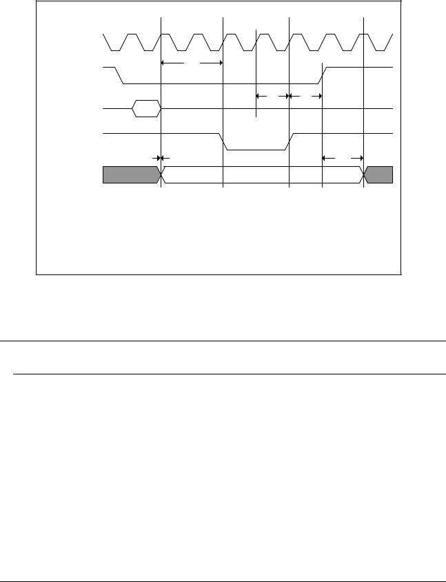
Figure 5-9: Stop Grant/Sleep Timing (SLP# assertion method)
|
Normal |
Stop Grant |
Sleep |
Stop Grant |
Normal |
BCLK |
|
|
|
|
|
|
|
Tv |
|
|
|
STPCLK# |
|
|
|
|
|
|
|
|
Tx |
Ty |
|
CPU bus |
stpgnt |
|
|
|
|
SLP# |
|
|
|
|
|
|
Tw |
|
|
Tz |
|
Compatibility |
Changing |
|
Frozen |
|
|
Signals |
|
|
|
||
|
|
|
|
|
NOTES:
Tv=T45 (Stop Grant Acknowledge Bus Cycle Completion to DPSLP# assertion)
Tw=T46 (Setup Time to Input Signal Hold Requirement)
Tx=T47 (Sleep PLL Lock Latency)
Ty=T48 (PLL lock to STPCLK# Hold Time)
Tz=T49 (Input Signal Hold Time)
5.2DC SPECIFICATIONS
5.2.1RECOMMENDED OPERATING CONDITIONS
Functional operation of the VIA Eden ESP processor is guaranteed if the conditions in Table 5-3 are met. Sustained operation outside of the recommended operating conditions may damage the device.
Table 5-7. Recommended Operating Conditions
PARAMETER |
MIN |
|
NOM |
MAX |
UNITS |
NOTES |
|
|
|
|
|
|
|
Operating Junction Temperature |
5 |
|
|
90 |
°C |
|
|
|
|
|
|
|
|
VCORE Voltage |
|
|
1.05 |
|
V |
Samuel 2 |
|
|
1.20 |
|
|||
|
|
|
|
|
|
|
|
|
|
|
|
|
|
VCORE Voltage |
|
|
1.10 |
|
V |
Ezra and Ezra-T |
|
|
|
|
|
|
|
VCORE Static Tolerance |
|
See Table 5-4 |
|
V |
(1) |
|
|
|
|
|
|
||
VCORE Dynamic Tolerance |
|
|
V |
(2) |
||
|
|
|
|
|||
|
|
|
|
|
|
|
VTT Voltage |
1.365 |
|
|
1.635 |
V |
Ezra |
|
|
|
|
|
|
|
VTT Voltage |
1.1375 |
|
1.25 |
|
V |
Ezra-T |
|
|
|
|
|
|
|
5-10 Electrical Specifications Section 5

Preliminary Information |
|
|
VIA Eden ESP Processor Datasheet |
||||
|
|
|
|
|
|
January 2002 |
|
|
|
|
|
|
|
|
|
|
RTT |
50 |
56 |
115 |
Ω |
(3) |
|
|
|
|
|
|
|
|
|
|
VREF |
-2% |
2/3 VTT |
+2% |
V |
|
|
|
|
|
|
|
|
|
|
Notes:
1.DC measurement
2.AC noise measured with bandwidth limited to 20MHz
3.Necessary for future VIA Eden processors. RTT is controlled by RTTCTRL ball. RTTCTRL should be 56Ω when relying upon on-die bus termination. RTTCTRL should be 110Ω when relying upon board termination.
Section 5 |
Electrical Specifications |
5-11 |

VIA Eden ESP Processor Datasheet |
|
|
|
Preliminary Information |
|||
January 2002 |
|
|
|
|
|
|
|
Table 5-8. VCC Static and Transient Tolerance |
|
|
|
||||
|
|
Voltage Deviation from VID Setting (mV) |
|
||||
|
|
Static Tolerance |
Transient Tolerance |
|
|||
|
Icc (A) |
Min |
Nom |
Max |
Min |
Max |
|
|
0 |
15 |
40 |
65 |
5 |
85 |
|
|
2 |
5 |
30 |
55 |
-5 |
74 |
|
|
4 |
-5 |
20 |
45 |
-15 |
62 |
|
|
6 |
-15 |
10 |
35 |
-25 |
51 |
|
|
8 |
-25 |
0 |
25 |
-35 |
40 |
|
|
10 |
-35 |
-10 |
15 |
-45 |
28 |
|
|
12 |
-45 |
-20 |
5 |
-55 |
17 |
|
|
14 |
-55 |
-30 |
-5 |
-65 |
6 |
|
|
16 |
-65 |
-40 |
-15 |
-76 |
-5 |
|
5.2.2 MAXIMUM RATINGS
While functional operation is not guaranteed beyond the operating ranges listed in Table 5-4, the device may be subjected to the limits specified in Table 5-5 without causing long-term damage.
These conditions must not be imposed on the device for a sustained period—any such sustained imposition may damage the device. Likewise exposure to conditions in excess of the maximum ratings may damage the device.
Table 5-9. Maximum Ratings
PARAMETER |
MIN |
MAX |
UNITS |
NOTES |
|
|
|
|
|
Operating Case Temperature |
5 |
85 |
°C |
|
|
|
|
|
|
Storage Temperature |
-65 |
150 |
°C |
|
|
|
|
|
|
Supply Voltage (VCC) |
-0.5 |
4.0 |
V |
|
|
|
|
|
|
CMOS I/O Voltage |
-0.5 |
2.0 |
V |
|
|
|
|
|
|
I/O Voltage |
-0.5 |
VTT +0.5 |
V |
|
|
|
|
|
|
5-12 |
Electrical Specifications |
Section 5 |

Preliminary Information |
VIA Eden ESP Processor Datasheet |
|
January 2002 |
5.2.3 DC CHARACTERISTICS
Table 5-10. DC Characteristics
PARAMETER |
MIN |
MAX |
UNITS |
NOTES |
|
|
|
|
|
IOL – Low level output current |
-9.0 |
|
mA |
@ V = VOL(max) |
|
|
|
|
|
VOH – High Level Output Voltage |
|
VTT |
V |
|
|
|
|
|
|
VOL – Low Level Output Voltage |
0 |
0.4 |
V |
@ Iol = -8mA |
|
|
|
|
|
IL – Input Leakage Current |
|
± 100 |
µA |
|
|
|
|
|
|
ILU – Input Leakage Current for inputs with pull-ups |
|
200 |
µA |
|
|
|
|
|
|
ILD – Input Leakage Current for inputs with pull-downs |
|
-400 |
µA |
|
|
|
|
|
|
Table 5-11. CMOS DC Characteristics
PARAMETER |
MIN |
MAX |
UNITS |
NOTES |
|
|
|
|
|
VIL -- Input Low Voltage |
-0.58 |
0.700 |
V |
|
|
|
|
|
|
VIH1.5 – Input High Voltage |
VREF + 0.2 |
VTT |
V |
(2) |
|
|
|
|
|
VIH2.5 – Input High Voltage |
2.0 |
3.18 |
V |
(3) |
|
|
|
|
|
VOL – Low Level Output Voltage |
|
0.40 |
V |
@ IOL |
|
|
|
|
|
VOH – High Level Output Voltage |
|
1.50 |
V |
(1) |
|
|
|
|
|
IOL – Low Level Output Current |
9 |
|
mA |
@ VOL |
|
|
|
|
|
ILI – Input Leakage Current |
|
±100 |
µA |
|
|
|
|
|
|
ILO – Output Leakage Current |
|
±100 |
µA |
|
|
|
|
|
|
Notes:
1.All CMOS signals are open drain.
2.Applies to all CMOS signals except BCLK.
3.Applies only to BCLK.
5.2.4 POWER DISSIPATION
Table 5-8 through Table 5-15 give the core power consumption for the VIA Eden ESP processor models. Note that this does not include the power consumed by the I/O pads.
Table 5-12. Normal Mode VCC Power Consumption
PARAMETER |
TYPICAL3,4 |
MAX1,2 |
UNITS |
NOTES |
PCC - Normal Mode Operating Power Con- |
|
|
|
|
sumption |
|
|
|
|
VIA Eden ESP 4000 (4.0 X 100 MHz) 1.05V |
1.7 |
3.0 |
W |
Samuel 2 |
VIA Eden ESP 5000 (4.0 X 133 MHz) 1.20V |
2.8 |
5.0 |
W |
Samuel 2 |
VIA Eden ESP 6000 (5.0 X 133 MHz) 1.10V |
2.8 |
5.0 |
W |
Ezra |
|
|
|
|
|
Notes:
1.100% tested. Consider these power numbers as the factory maximum. The factory will reject processors that exceed these values.
Section 5 |
Electrical Specifications |
5-13 |

VIA Eden ESP Processor Datasheet |
Preliminary Information |
January 2002
2.The above power consumption is preliminary and based on 90°C junction and 1.10 (Ezra) or 1.20/1.05 (Samuel 2) Volts.
3.Typical power is defined as the average power dissipated while running WinStone99 onWin98. Contact your VIA Sales Representative for further information.
4.Thermal solutions must be designed to account for worst-case core and I/O power consumption.
Table 5-13. StopGrant VCC Power Consumption
PARAMETER |
MAX1,2 |
UNITS |
NOTES |
PCC – StopGrant / AutoHalt Mode Operating |
|
|
No snooping activity |
Power Consumption |
|
|
|
|
|
|
|
VIA Eden ESP 4000 (4.0 X 100 MHz) 1.05V |
1.00 |
W |
Samuel 2 |
VIA Eden ESP 5000 (4.0 X 133 MHz) 1.20V |
1.00 |
W |
Samuel 2 |
VIA Eden ESP 6000 (5.0 X 133 MHz) 1.10V |
TBD |
W |
Ezra |
|
|
|
|
Notes:
1.100% tested. Consider these power numbers as the factory maximum. The factory will reject processors that exceed these values.
2.The above power consumption is preliminary and based on 90°C junction and 1.10 (Ezra) or 1.20/1.05 (Samuel 2) Volts.
Table 5-14. Sleep VCC Power Consumption
PARAMETER |
MAX1 |
UNITS |
NOTES |
PCC – Sleep Mode Operating Power Consump- |
|
|
|
tion |
|
|
|
VIA Eden ESP 4000 (4.0 X 100 MHz) 1.05V |
1.00 |
W |
Samuel 2 |
VIA Eden ESP 5000 (4.0 X 133 MHz) 1.20V |
1.00 |
W |
Samuel 2 |
VIA Eden ESP 6000 (5.0 X 133 MHz) 1.10V |
TBD |
W |
Ezra |
|
|
|
|
Notes:
1.100% tested. Consider these power numbers as the factory maximum. The factory will reject processors that exceed these values.
2.The above power consumption is preliminary and based on 90°C junction and 1.10 (Ezra) or 1.20/1.05 (Samuel 2) Volts.
Table 5-15. Deep Sleep VCC Power Consumption
PARAMETER |
MAX1 |
UNITS |
NOTES |
PCC – Deep Sleep Mode Operating Power |
|
|
|
Consumption |
|
|
|
VIA Eden ESP 4000 (4.0 X 100 MHz) 1.05V |
0.87 |
W |
Samuel 2 |
VIA Eden ESP 5000 (4.0 X 133 MHz) 1.20V |
0.87 |
W |
Samuel 2 |
VIA Eden ESP 6000 (5.0 X 133 MHz) 1.10V |
TBD |
W |
Ezra |
|
|
|
|
Notes:
1.100% tested. Consider these power numbers as the factory maximum. The factory will reject processors that exceed these values.
2.The above power consumption is preliminary and based on 90°C junction and 1.10 (Ezra) or 1.20/1.05 (Samuel 2) Volts.
5-14 |
Electrical Specifications |
Section 5 |
Preliminary Information |
|
|
|
VIA Eden ESP Processor Datasheet |
||||
|
|
|
|
|
|
|
|
January 2002 |
Table 5-16. VSS-I/O Power Consumption |
|
|
|
|
||||
|
PARAMETER |
|
TYPICAL |
|
MAX |
UNITS |
NOTES |
|
|
|
|
|
|
||||
|
Pss-I/O – I/O Operating |
|
300 |
|
820 |
mW |
|
|
|
Power Consumption |
|
|
|
|
|
|
|
Section 5 |
Electrical Specifications |
5-15 |