

XE167x
XE166 Family Derivatives
Electrical Parameters
4.6AC Parameters
These parameters describe the dynamic behavior of the XE167.
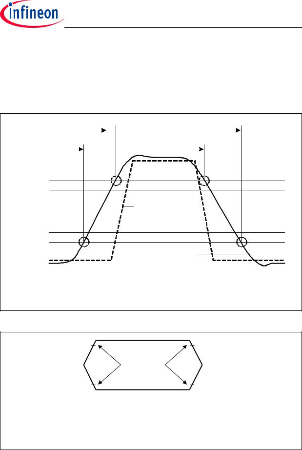
4.6.1Testing Waveforms
These values are used for characterization and production testing (except pin XTAL1).
Output delay |
Output delay |
Hold time |
Hold time |
0.8 VDDP
0.7 VDDP
Input Signal (driven by tester)
0.3 VDDP
0.2 VDDP Output Signal
(measured)
Output timings refer to the rising edge of CLKOUT.
Input timings are calculated from the time, when the input signal reaches VIH or VIL, respectively.
MCD05556C
Figure 16 Input Output Waveforms
VLoad + 0.1 |
V |
VOH - 0.1 V |
|
|
|
Timing |
|
|
|
Reference |
|
|
|
|
|
|
|
Points |
|
VLoad - 0.1 |
V |
VOL + 0.1 V |
|
For timing purposes a port pin is no longer floating when a 100 mV change from load voltage occurs, but begins to float when a 100 mV change from the loaded VOH /VOL level occurs (IOH / IOL = 20 mA).
MCA05565
Figure 17 Floating Waveforms
Data Sheet |
93 |
V2.1, 2008-08 |

XE167x
XE166 Family Derivatives
Electrical Parameters
4.6.2Definition of Internal Timing
The internal operation of the XE167 is controlled by the internal system clock fSYS.
Because the system clock signal fSYS can be generated from a number of internal and external sources using different mechanisms, the duration of the system clock periods
(TCSs) and their variation (as well as the derived external timing) depend on the mechanism used to generate fSYS. This must be considered when calculating the timing for the XE167.
Phase Locked Loop Operation (1:N) |
fIN |
fSYS |
TCS |
Direct Clock Drive (1:1) |
fIN |
fSYS |
TCS |
Prescaler Operation (N:1) |
fIN |
fSYS |
TCS |
MC_XC2X_CLOCKGEN |
Figure 18 Generation Mechanisms for the System Clock
Note: The example of PLL operation shown in Figure 18 uses a PLL factor of 1:4; the example of prescaler operation uses a divider factor of 2:1.
The specification of the external timing (AC Characteristics) depends on the period of the system clock (TCS).
Data Sheet |
94 |
V2.1, 2008-08 |

XE167x
XE166 Family Derivatives
Electrical Parameters
Direct Drive
When direct drive operation is selected (SYSCON0.CLKSEL = 11B), the system clock is derived directly from the input clock signal CLKIN1:
fSYS = fIN.
The frequency of fSYS is the same as the frequency of fIN. In this case the high and low times of fSYS are determined by the duty cycle of the input clock fIN.
Selecting Bypass Operation from the XTAL11) input and using a divider factor of 1 results in a similar configuration.
Prescaler Operation
When prescaler operation is selected (SYSCON0.CLKSEL = 10B, PLLCON0.VCOBY = 1B), the system clock is derived either from the crystal oscillator (input clock signal
XTAL1) or from the internal clock source through the output prescaler K1 (= K1DIV+1):
fSYS = fOSC / K1.
If a divider factor of 1 is selected, the frequency of fSYS equals the frequency of fOSC. In this case the high and low times of fSYS are determined by the duty cycle of the input
clock fOSC (external or internal).
The lowest system clock frequency results from selecting the maximum value for the divider factor K1:
fSYS = fOSC / 1024.
Phase Locked Loop (PLL)
When PLL operation is selected (SYSCON0.CLKSEL = 10B, PLLCON0.VCOBY = 0B), the on-chip phase locked loop is enabled and provides the system clock. The PLL multiplies the input frequency by the factor F (fSYS = fIN × F).
F is calculated from the input divider P (= PDIV+1), the multiplication factor N (=
NDIV+1), and the output divider K2 (= K2DIV+1):
(F = N / (P × K2)).
The input clock can be derived either from an external source at XTAL1 or from the onchip clock source.
The PLL circuit synchronizes the system clock to the input clock. This synchronization is performed smoothly so that the system clock frequency does not change abruptly.
Adjustment to the input clock continuously changes the frequency of fSYS so that it is locked to fIN. The slight variation causes a jitter of fSYS which in turn affects the duration of individual TCSs.
1) Voltages on XTAL1 must comply to the core supply voltage VDDI1.
Data Sheet |
95 |
V2.1, 2008-08 |

XE167x
XE166 Family Derivatives
Electrical Parameters
The timing in the AC Characteristics refers to TCSs. Timing must be calculated using the minimum TCS possible under the given circumstances.
The actual minimum value for TCS depends on the jitter of the PLL. Because the PLL is constantly adjusting its output frequency to correspond to the input frequency (from crystal or oscillator), the accumulated jitter is limited. This means that the relative deviation for periods of more than one TCS is lower than for a single TCS (see formulas and Figure 19).
This is especially important for bus cycles using waitstates and for the operation of timers, serial interfaces, etc. For all slower operations and longer periods (e.g. pulse train generation or measurement, lower baudrates, etc.) the deviation caused by the PLL jitter is negligible.
The value of the accumulated PLL jitter depends on the number of consecutive VCO output cycles within the respective timeframe. The VCO output clock is divided by the output prescaler K2 to generate the system clock signal fSYS. The number of VCO cycles is K2 × T, where T is the number of consecutive fSYS cycles (TCS).
The maximum accumulated jitter (long-term jitter) DTmax is defined by:
DTmax [ns] = ±(220 / (K2 × fSYS) + 4.3)
This maximum value is applicable, if either the number of clock cycles T > (fSYS / 1.2) or the prescaler value K2 > 17.
In all other cases for a timeframe of T × TCS the accumulated jitter DT is determined by:
DT [ns] = DTmax × [(1 - 0.058 × K2) × (T - 1) / (0.83 × fSYS - 1) + 0.058 × K2] fSYS in [MHz] in all formulas.
Example, for a period of 3 TCSs @ 33 MHz and K2 = 4:
Dmax = ±(220 / (4 × 33) + 4.3) = 5.97 ns (Not applicable directly in this case!)
D3 = 5.97 × [(1 - 0.058 × 4) × (3 - 1) / (0.83 × 33 - 1) + 0.058 × 4]
=5.97 × [0.768 × 2 / 26.39 + 0.232]
=1.7 ns
Example, for a period of 3 TCSs @ 33 MHz and K2 = 2:
Dmax = ±(220 / (2 × 33) + 4.3) = 7.63 ns (Not applicable directly in this case!) D3 = 7.63 × [(1 - 0.058 × 2) × (3 - 1) / (0.83 × 33 - 1) + 0.058 × 2]
=7.63 × [0.884 × 2 / 26.39 + 0.116]
=1.4 ns
Data Sheet |
96 |
V2.1, 2008-08 |

XE167x
XE166 Family Derivatives
Electrical Parameters
Acc. jitter DT |
|
|
|
|
|
|
ns |
|
fSYS = 33 MHz |
fSYS = 66 MHz |
|
||
±9 |
|
|
||||
|
|
|
|
|
||
±8 |
|
|
|
|
fVCO = 66 MHz |
|
±7 |
|
|
|
fVCO = 132 MHz |
||
±6 |
|
|
|
|||
|
|
|
|
|
||
±5 |
|
|
|
|
|
|
±4 |
|
|
|
|
|
|
±3 |
|
|
|
|
|
|
±2 |
|
|
|
|
|
|
±1 |
|
|
|
|
Cycles T |
|
0 |
|
|
|
|
||
20 |
40 |
60 |
80 |
100 |
||
1 |
||||||
MC_XC2X_JITTER
Figure 19 Approximated Accumulated PLL Jitter
Note: The specified PLL jitter values are valid if the capacitive load per pin does not exceed CL = 20 pF (see Table 12).
The maximum peak-to-peak noise on the pad supply voltage (measured between
VDDPB pin 100/144 and VSS pin 1) is limited to a peak-to-peak voltage of VPP = 50 mV. This can be achieved by appropriate blocking of the supply voltage as
close as possible to the supply pins and using PCB supply and ground planes.
Different frequency bands can be selected for the VCO so that the operation of the PLL can be adjusted to a wide range of input and output frequencies:
Table 25 |
VCO Bands for PLL Operation1) |
|
|
PLLCON0.VCOSEL |
VCO Frequency Range |
Base Frequency Range |
|
|
|
|
|
00 |
|
50 … 110 MHz |
10 … 40 MHz |
|
|
|
|
01 |
|
100 … 160 MHz |
20 … 80 MHz |
|
|
|
|
1X |
|
Reserved |
|
|
|
|
|
1) Not subject to production test - verified by design/characterization.
Data Sheet |
97 |
V2.1, 2008-08 |

XE167x
XE166 Family Derivatives
Electrical Parameters
Wakeup Clock
When wakeup operation is selected (SYSCON0.CLKSEL = 00B), the system clock is derived from the low-frequency wakeup clock source:
fSYS = fWU.
In this mode, a basic functionality can be maintained without requiring an external clock source and while minimizing the power consumption.
Selecting and Changing the Operating Frequency
When selecting a clock source and the clock generation method, the required parameters must be carefully written to the respective bitfields, to avoid unintended intermediate states.
Many applications change the frequency of the system clock (fSYS) during operation in order to optimize system performance and power consumption. Changing the operating frequency also changes the switching currents, which influences the power supply.
To ensure proper operation of the on-chip EVRs while they generate the core voltage, the operating frequency shall only be changed in certain steps. This prevents overshoots and undershoots of the supply voltage.
To avoid the indicated problems, recommended sequences are provided which ensure the intended operation of the clock system interacting with the power system.
Please refer to the Programmer’s Guide.
Data Sheet |
98 |
V2.1, 2008-08 |