

Philips Semiconductors Linear Products |
Product specification |
|
|
|
|
Tone decoder/phase-locked loop |
NE/SE567 |
|
|
|
|
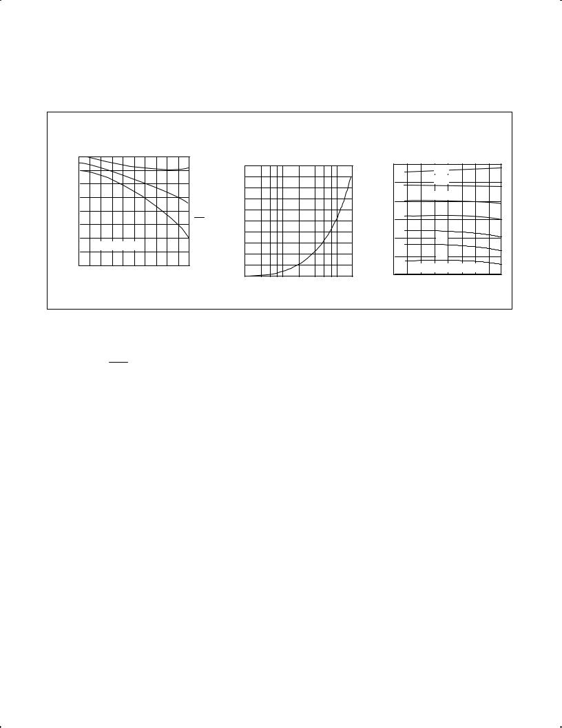
TYPICAL PERFORMANCE CHARACTERISTICS (Continued)
Center Frequency Temperature |
Center Frequency |
Typical Bandwidth Variation |
|
Shift With Supply |
|||
Coefficient |
|||
Voltage Change vs |
Temperature |
||
(Mean and SD) |
|||
Operating Frequency |
|
||
|
|
C |
100 |
|
|
|
|
|
ppm/ ° |
|
|
|
|
|
|
COEFFICIENTÐ |
0 |
|
|
|
|
|
±100 |
|
|
|
|
|
|
|
|
|
|
|
|
|
TEMPERATURE |
±200 |
|
|
|
|
|
|
t = 0°C to 70°C |
|
|
|
||
±300 |
|
|
|
|
|
|
|
4.5 |
5.0 |
5.5 |
6.0 |
6.5 |
7.0 |
SUPPLY VOLTAGE Ð V
|
|
1.0 |
|
|
|
|
|
|
|
|
|
15.0 |
|
|
14 |
|
|
|
|
0.9 |
|
|
|
|
|
|
|
|
|
12.5 |
|
|
12 |
|
|
|
|
0.8 |
|
|
|
|
|
|
|
|
|
|
|
|
|
|
|
|
|
|
|
|
|
|
|
|
|
O |
|
|
|
10 |
|
|
|
|
|
|
|
|
|
|
|
|
|
|
|
|
|
|
|
||
|
|
0.7 |
|
|
|
|
|
|
|
|
f |
|
|
|
|
|
|
|
|
|
|
|
|
|
|
|
|
OF |
10.0 |
|
|
|
|
|
|
|
|
|
|
|
|
|
|
|
|
|
|
|
8 |
|
|
||
|
|
|
|
|
|
|
|
|
|
|
|
|
|
|
|
||
tO |
0.6 |
|
|
|
|
|
|
|
|
% |
|
|
|
|
|
||
|
|
|
|
|
|
|
|
|
|
|
|
|
|
||||
t |
|
V * % V |
|
|
|
|
|
|
|
|
Ð |
7.5 |
|
|
|
|
|
O |
0.5 |
|
|
|
|
|
|
|
|
BANDWIDTH |
|
|
6 |
|
|
||
|
|
|
|
|
|
|
|
|
|
|
|
|
|
|
|||
|
|
0.4 |
|
|
|
|
|
|
|
|
5.0 |
|
|
|
|
|
|
|
|
0.3 |
|
|
|
|
|
|
|
|
|
|
|
4 |
|
|
|
|
|
|
|
|
|
|
|
|
|
|
|
|
|
|
|
|
|
|
|
0.2 |
|
|
|
|
|
|
|
|
|
2.5 |
|
|
2 |
|
|
|
|
|
|
|
|
|
|
|
|
|
|
|
|
|
|
|
|
|
|
0.1 |
|
|
|
|
|
|
|
|
|
|
BANDWIDTH AT 25°C |
|
|||
|
|
|
|
|
|
|
|
|
|
|
|
0 |
|
||||
|
|
0 |
|
|
|
|
|
|
|
|
|
|
|
|
|
|
|
|
|
|
|
|
|
|
|
|
|
|
|
|
|
|
|
|
|
|
|
1 |
2 |
3 |
4 |
5 |
10 |
20 |
40 |
100 |
|
±75 |
±25 |
0 |
25 |
75 |
125 |
|
|
|
|
CENTER FREQUENCY Ð kHz |
|
|
|
|
TEMPERATURE ± °C |
|
|||||||
DESIGN FORMULAS
fO |
[ |
1 |
|
|
|
|
|
1.1R1 |
C1 |
|
|
||||
|
|
|
|
||||
|
|
|
|||||
BW [ 1070 VI |
in % of fO |
||||||
|
|
|
|
fO |
C2 |
||
VI v 200mVRMS
Where
VI=Input voltage (VRMS)
C2=Low-pass filter capacitor (μF)
PHASE-LOCKED LOOP TERMINOLOGY CENTER FREQUENCY (fO)
The free-running frequency of the current controlled oscillator (CCO) in the absence of an input signal.
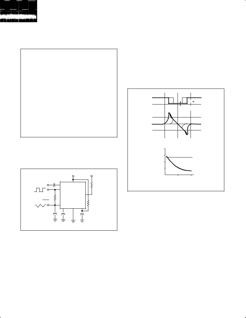
OPERATING INSTRUCTIONS
Figure 1 shows a typical connection diagram for the 567. For most applications, the following three-step procedure will be sufficient for choosing the external components R1, C1, C2 and C3.
1.Select R1 and C1 for the desired center frequency. For best temperature stability, R1 should be between 2K and 20K ohm, and the combined temperature coefficient of the R1C1 product should have sufficient stability over the projected temperature range to meet the necessary requirements.
2.Select the low-pass capacitor, C2, by referring to the Bandwidth versus Input Signal Amplitude graph. If the input amplitude Variation is known, the appropriate value of fO C2 necessary to give the desired bandwidth may be found. Conversely, an area of operation may be selected on this graph and the input level and
C2 may be adjusted accordingly. For example, constant bandwidth operation requires that input amplitude be above
200mVRMS. The bandwidth, as noted on the graph, is then controlled solely by the fO C2 product (fO (Hz), C2(μF)).
Detection Bandwidth (BW)
The frequency range, centered about fO, within which an input signal above the threshold voltage (typically 20mVRMS) will cause a logical zero state on the output. The detection bandwidth corresponds to the loop capture range.
Lock Range
The largest frequency range within which an input signal above the threshold voltage will hold a logical zero state on the output.
Detection Band Skew
A measure of how well the detection band is centered about the
center frequency, fO. The skew is defined as (fMAX+fMIN-2fO)/2fO where fmax and fmin are the frequencies corresponding to the
edges of the detection band. The skew can be reduced to zero if necessary by means of an optional centering adjustment.
April 15, 1992 |
408 |
Philips Semiconductors Linear Products |
Product specification |
|
|
|
|
Tone decoder/phase-locked loop |
NE/SE567 |
|
|
|
|
TYPICAL RESPONSE
INPUT
OUTPUT
NOTE:
RL = 100Ω
Response to 100mVRMS Tone Burst
OUTPUT
INPUT
NOTES:
S/N = ±6dB
RL = 100Ω
Noise Bandwidth = 140Hz
Response to Same Input Tone Burst
With Wideband Noise
3.The value of C3 is generally non-critical. C3 sets the band edge of a low-pass filter which attenuates frequencies outside the detection band to eliminate spurious outputs. If C3 is too small, frequencies just outside the detection band will switch the output stage on and off at the beat frequency, or the output may pulse on and off during the turn-on transient. If C3 is too large, turn-on and turn-off of the
|
|
+V |
+V |
INPUT |
3 |
4 |
RL |
|
|||
|
5 |
|
|
|
567 |
8 |
|
1 |
R1 |
|
|
fO R1C1 |
6 |
|
R2 |
|
|
||
|
2 |
7 |
1 |
|
C2 |
|
C3 |
|
C1 |
|
|
|
LOW |
|
OUTPUT |
|
PASS |
|
FILTER |
|
FILTER |
||
|
|
||
Figure 1.
saturates; its collector voltage being less than 1.0 volt (typically
0.6V) at full output current (100mA). The voltage at Pin 2 is the phase detector output which is a linear function of frequency over the range of 0.95 to 1.05 fO with a slope of about 20mV per percent of frequency deviation. The average voltage at Pin 1 is, during lock, a function of the in-band input amplitude in accordance with the transfer characteristic given. Pin 5 is the controlled oscillator square wave output of magnitude (+V -2VBE) (+V-1.4V) having a DC average of +V/2. A 1kΩ load may be driven from pin 5. Pin 6 is an exponential triangle of 1VP-P with an average DC level of +V/2. Only high impedance loads may be
OUTPUT |
V+ |
|
(PIN 8) |
||
7% 14% BW |
||
|
||
|
0 |
|
|
VCE (SAT) < 1.0V |
|
|
3.9V |
LOW PASS
FILTER 3.8V (PIN 2)
3.7V
0.9fO |
fO |
1.1fO |
PIN 1 |
|
|
VOLTAGE |
|
|
(AVG) 4.0 |
|
VREF |
THRESHOLD VOLTAGE |
||
3.5 |
|
|
3.0 |
|
|
f1 = fO |
|
|
2.5 |
|
|
0 |
100 |
200mVrms |
IN-BAND |
|
|
INPUT |
|
|
VOLTAGE |
|
|
Figure 2. Typical Output Response
output stage will be delayed until the voltage on C3 passes the threshold voltage. (Such delay may be desirable to avoid spurious outputs due to transient frequencies.) A typical minimum value for C3 is 2C2.
4.Optional resistor R2 sets the threshold for the largest ªno outputº input voltage. A value of 130kΩ is used to assure the tested limit
of 10mVRMS min. This resistor can be referenced to ground for increased sensitivity. The explanation can be found in the
ªoptional controlsº section which follows.
AVAILABLE OUTPUTS (Figure 1)
The primary output is the uncommitted output transistor collector, Pin 8. When an in-band input signal is present, this transistor
April 15, 1992 |
409 |

Philips Semiconductors Linear Products |
Product specification |
|
|
|
|
Tone decoder/phase-locked loop |
NE/SE567 |
|
|
|
|
|
V+ |
|
|
|
|
R |
|
|
|
567 |
1 |
567 |
1 |
|
|
C3 |
|
R |
|
|
|
|
C3 |
|
DECREASE |
INCREASE |
|||
SENSITIVITY |
||||
SENSITIVITY |
||||
|
|
|||
|
V+ |
|
RA |
DECREASE |
|
SENSITIVITY |
||
567 1 |
RB |
|
50k |
2.5k |
|
INCREASE |
||
C3 |
||
SENSITIVITY |
||
|
RC |
|
|
1.0k |
|
|
SILICON |
|
|
DIODES FOR |
|
|
TEMPERATURE |
|
|
COMPENSATION |
|
|
(OPTIONAL) |
Figure 3. Sensitivity Adjust
connected to pin 6 without affecting the CCO duty cycle or temperature stability.
OPERATING PRECAUTIONS
A brief review of the following precautions will help the user achieve the high level of performance of which the 567 is capable.
1.Operation in the high input level mode (above 200mV) will free the user from bandwidth variations due to changes in the in-band signal amplitude. The input
stage is now limiting, however, so that out-band signals or high noise levels can cause an apparent bandwidth reduction as the inband signal is suppressed. Also, the limiting action will create in-band components from sub-harmonic signals, so the 567 becomes sensitive to signals at fO/3, fO/5, etc.
2.The 567 will lock onto signals near (2n+1) fO, and will give an output for signals near (4n+1) fO where n=0, 1, 2, etc. Thus, signals at 5fO and 9fO can cause an unwanted output. If such signals are anticipated, they should be attenuated before reaching the 567 input.
3.Maximum immunity from noise and out-band signals is afforded
in the low input level (below 200mVRMS) and reduced bandwidth operating mode. However, decreased loop damping causes the
worst-case lock-up time to increase, as shown by the Greatest Number of Cycles Before Output vs Bandwidth graph.
4.Due to the high switching speeds (20ns) associated with 567 operation, care should be taken in lead routing. Lead lengths
should be kept to a minimum. The power supply should be adequately bypassed close to the 567 with a 0.01μF or greater capacitor; grounding paths should be carefully chosen to avoid ground loops and unwanted voltage variations. Another factor which must be considered is the effect of load energization on the power supply. For example, an incandescent lamp typically draws 10 times rated current at turn-on. This can be somewhat greater when the output stage is made less sensitive, rejection of third harmonics or in-band harmonics (of lower frequency signals) is also improved.
cause supply voltage fluctuations which could, for example, shift the detection band of narrow-band systems sufficiently to cause momentary loss of lock. The result is a low-frequency oscillation into and out of lock. Such effects can be prevented by supplying heavy load currents from a separate supply or increasing the supply filter capacitor.
SPEED OF OPERATION
Minimum lock-up time is related to the natural frequency of the loop.
The lower it is, the longer becomes the turn-on transient. Thus, maximum operating speed is obtained when C2 is at a minimum. When the signal is first applied, the phase may be such as to initially drive the controlled oscillator away from the incoming frequency rather than toward it. Under this condition, which is of course unpredictable, the lock-up transient is at its worst and the theoretical minimum lock-up time is not achievable. We must simply wait for the transient to die out.
The following expressions give the values of C2 and C3 which allow highest operating speeds for various band center frequencies. The minimum rate at which digital information may be detected without information loss due to the turn-on transient or output chatter is about 10 cycles per bit, corresponding to an information transfer rate of fO/10 baud.
|
V+ |
|
|
V+ |
V+ |
V+ |
|
|
|
|
|
||
|
|
RL |
|
|
|
RA |
|
|
|
RL |
|
200 TO 1k |
|
|
|
|
|
|
|
|
567 |
8 |
|
567 |
8 |
|
|
1 |
|
Cf |
1 |
Rf |
|
Rf RL |
|
|
|
|
|||
|
|
|
1 |
10k |
||
|
|
|
|
10k |
|
|
|
Rf* |
|
|
C3 |
567 |
8 |
C3 |
|
|
|
|||
10k |
|
|
|
|
|
|
|
|
|
|
RA |
|
|
*OPTIONAL - PERMITS |
|
200 TO |
|
|
||
|
1k |
|
|
|||
LOWER VALUE OF Cf |
|
|
|
|||
|
|
|
|
|||
|
Figure 4. Chatter Prevention |
|
||||
|
|
|
V+ |
|
|
|
|
|
|
R |
|
|
|
|
567 |
2 |
|
567 |
2 |
|
|
|
|
C2 |
|
|
R |
|
LOWERS fO |
|
|
C2 |
||
|
|
RAISES fO |
|
|||
RA
567 1
50k

 C2 RAISES fO
V+ |
|
|
LOWERS fO |
RB |
|
2.5k |
|
RC |
RAISES fO |
1.0k |
|
|
SILICON |
|
DIODES FOR |
|
TEMPERATURE |
|
COMPENSATION |
|
(OPTIONAL) |
Figure 5. Skew Adjust
April 15, 1992 |
410 |

Philips Semiconductors Linear Products |
Product specification |
|
|
|
|
Tone decoder/phase-locked loop |
NE/SE567 |
|
|
|
|
130
C2 + fO mF
260
C3 + fO mF
In cases where turn-off time can be sacrificed to achieve fast turn-on, the optional sensitivity adjustment circuit can be used to move the quiescent C3 voltage lower (closer to the threshold voltage). However, sensitivity to beat frequencies, noise and extraneous signals will be increased.
OPTIONAL CONTROLS (Figure 3)
The 567 has been designed so that, for most applications, no external adjustments are required. Certain applications, however, will be greatly facilitated if full advantage is taken of the added control possibilities available through the use of additional external components. In the diagrams given, typical
values are suggested where applicable. For best results the resistors used, except where noted, should have the same temperature coefficient. Ideally, silicon diodes would be low-resistivity types, such as forward-biased transistor base-emitter junctions. However, ordinary low-voltage diodes should be adequate for most applications.
|
250 |
|
|
|
|
|
|
|
|
|
|
|
0.5k |
0.9k |
1.4k |
|
1.9k |
2.5k |
3.2k |
4.0k |
|
Ð RMS |
200 |
|
|
|
|
|
|
|
|
|
|
|
|
|
|
|
|
|
10k |
|
|
MV |
150 |
|
|
|
|
|
|
|
|
|
|
|
|
|
|
|
|
|
|
||
|
|
|
|
|
|
|
|
|
|
|
VOLTAGE |
|
|
|
|
|
|
|
|
20k |
|
100 |
|
|
|
|
|
|
|
|
|
|
|
|
|
|
|
|
|
100k |
|
||
INPUT |
|
|
|
|
|
|
|
|
||
50 |
|
|
|
|
|
|
|
R |
|
|
|
|
|
|
|
|
|
|
|
||
|
|
|
|
|
|
|
|
|
|
|
|
0 |
2 |
|
4 |
6 |
8 |
10 |
12 |
14 |
16 |
|
0 |
|
||||||||
|
|
|
DETECTION BAND Ð % OF fO |
|
||||||
RA
50k
PIN 2 567
C2
V+
RB
RBRC
R + R )
A RB ) RC
RC
OPTIONAL SILICON
DIODES FOR
TEMPERATURE
COMPENSATION
NOTE: |
|
|
|
|
|
|
|
||
130 |
10k |
R |
|
|
1300 |
10k R |
|
||
f |
|
) |
|
|
f |
|
) |
|
|
O |
|
R |
t C2 |
t |
O |
R |
|
||
|
|
|
|
|
|
|
|
||
Adjust control for symmetry of detection band edges about fO.
Figure 6. BW Reduction
SENSITIVITY ADJUSTMENT (Figure 3)
When operated as a very narrow-band detector (less than 8 percent), both C2 and C3 are made quite large in order to improve noise and out-band signal rejection. This will inevitably slow the response time. If, however, the output stage is biased closer to the threshold level, the turn-on time can be
improved. This is accomplished by drawing additional current to terminal 1. Under this condition, the 567 will also give an output for lower-level signals (10mV or lower).
By adding current to terminal 1, the output stage is biased further away from the threshold voltage. This is most useful when, to obtain maximum operating speed, C2 and C3 are made very small.
Normally, frequencies just outside the detection band could cause false outputs under this condition. By desensitizing the output stage, the out-band beat notes do not feed through to the output stage.
Since the input level must
V+ |
V+ |
|
RL |
567 |
8 |
1 |
|
RA |
|
10k |
|
|
Rf |
CA |
20k |
C3 |
UNLATCH
|
V+ |
V+ |
RL |
|
|
567 |
8 |
UNLATCH |
|
1 |
|
|
Rf |
|
20k |
|
C3 |
NOTE:
CA prevents latch-up when power supply is turned on.
Figure 7. Output Latching
April 15, 1992 |
411 |