

analog_system_lab_pro_manual
.pdfAnalog
System
Lab Kit PRO
MANUAL


Table of contents
Introduction |
|
9 |
|
Analog System Lab |
10 |
||
Organization of the Analog System Lab Course |
11 |
||
Lab Setup |
|
12 |
|
System Lab Kit ASLK PRO - An overview |
13 |
||
|
Hardware |
13 |
|
|
Software |
|
13 |
Getting to know ASLK PRO |
14 |
||
Organization of the Manual |
16 |
||
Experiment 1: |
17 |
||
Study the characteristics of negative feedback amplifiers and |
|
||
design of an instrumentation amplifier |
|
||
1.1 |
Brief theory and motivation |
18 |
|
|
1.1.1 |
Unity Gain Amplifier |
18 |
|
1.1.2 |
Non-inverting Amplifier |
19 |
|
1.1.3 |
Inverting Amplifier |
19 |
1.2 |
Exercise Set 1 |
20 |
|
1.3 |
Measurements to be taken |
20 |
|
1.4 |
What should you submit |
21 |
|
1.5 |
Other related ICs |
21 |
|
Experiment 2: |
|
23 |
|
Study the characteristics of regenerative feedback system with |
|
||
extension to design an astable and monostable multivibrator |
|
||
2.1 |
Brief theory and motivation |
24 |
|
 Analog System Lab Kit PRO
|
2.1.1 |
Inverting Regenerative Comparator |
24 |
|
2.1.2 |
Astable Multivibrator |
24 |
|
2.1.3 |
Monostable Multivibrator (Timer) |
25 |
2.2 |
Exercise Set 2 |
26 |
|
Experiment 3: |
|
27 |
|
Study the characteristics of integrators and differentiator circuits |
|
||
3.1 |
Brief theory and motivation |
28 |
|
|
3.1.1 |
Integrators |
28 |
|
3.1.2 |
Differentiators |
28 |
3.2 |
Specifications |
28 |
|
3.3 |
Measurements to be taken |
28 |
|
3.4 |
What should you submit |
29 |
|
3.5Exercise Set 3 - Grounded Capacitor Topologies
|
of Integrator and Differentiator |
30 |
Experiment 4: |
31 |
|
Design of Analog Filters |
|
|
4.1 |
Brief theory and motivation |
32 |
4.2 |
Specification |
33 |
4.3 |
Measurements to be taken |
33 |
4.4 |
What should you submit |
33 |
4.5 |
Exercise Set 4 |
34 |
page 3

Table of contents
Experiment 5:
Design of a self-tuned filter
5.1Brief theory and motivation
5.1.1Multiplier as a Phase Detector
5.2Specification
5.3Measurements to be taken
5.3.1Transient response
5.4What should you submit
5.4.1Exercise Set 5
Experiment 6:
Design a function generator and convert it to Voltage-Controlled Oscillator/FM Generator
6.1Brief theory and motivation
6.2Specifications
6.3Measurements to be taken
6.4What should you submit
6.5Exercise Set 6
Experiment 7:
Design of a Phase Lock Loop (PLL)
7.1Brief theory and motivation
7.2Specifications
7.3Measurements to be taken
7.4What should you submit
7.5Exercise Set 7
page 4
35 |
Experiment 8: |
|
47 |
||
|
Automatic Gain Control (AGC) Automatic Volume Control (AVC) |
|
|||
36 |
8.1 |
Brief theory and motivation |
48 |
||
36 |
|||||
8.2 |
Specifications |
48 |
|||
37 |
|||||
8.3 |
Measurements to be taken |
48 |
|||
37 |
|||||
8.4 |
What should you submit |
48 |
|||
37 |
|||||
8.5 |
Exercise Set 8 |
49 |
|||
37 |
|||||
|
|
|
|
||
38 |
|
|
|
|
|
39 |
Experiment 9: |
|
51 |
||
DC-DC Converter |
|
|
|||
|
|
|
|||
|
9.1 |
Brief theory and motivation |
52 |
||
|
9.2 |
Specification |
52 |
||
40 |
9.3 |
Measurements to be taken |
52 |
||
|
9.3.1 |
Time response |
52 |
||
40 |
|
||||
|
9.3.2 |
Transfer function |
52 |
||
40 |
|
||||
9.4 |
What should you submit |
53 |
|||
41 |
|||||
9.5 |
Exercise Set 9 |
53 |
|||
41 |
|||||
|
|
|
|
||
43 |
Experiment 10: |
55 |
|||
|
Design a Low Dropout (LDO) regulator |
|
|||
44 |
10.1 |
Brief theory and motivation |
56 |
||
44 |
10.2 |
Specifications |
56 |
||
45 |
10.3 |
Measurements to be taken |
56 |
||
45 |
10.4 |
What should you submit |
57 |
||
45 |
10.5 |
Exercise Set 10 |
57 |
||
Analog System Lab Kit PRO 

Table of contents
Experiment 11: |
59 |
|
To study the parameters of an LDO integrated circuit |
|
|
11.1 |
Brief theory and motivation |
60 |
11.2 |
Specifications |
60 |
11.3 |
Measurements to be taken |
60 |
11.4 |
What should you submit |
61 |
Experiment 12: |
63 |
|
To study the parameters of a DC-DC Converter using on-board |
|
|
Evaluation module |
|
|
12.1 |
Brief theory and motivation |
64 |
12.2 |
Specifications |
65 |
12.3 |
Measurements to be taken |
65 |
12.4 |
What should you submit |
65 |
Experiment 13: |
67 |
|
Design of a Digitally Controlled Gain Stage Amplifier |
|
|
13.1 |
Brief theory and motivation |
68 |
13.2 |
Specifications |
68 |
13.3 |
Measurements to be taken |
68 |
13.4 |
What should you submit |
68 |
13.5 |
Exercise Set 13 |
69 |
Experiment 14: |
71 |
|
Design of a Digitally Programmable Square and Triangular wave |
|
|
generator/oscillator |
|
|
14.1 |
Brief theory and motivation |
72 |
 Analog System Lab Kit PRO
14.2 |
Specifications |
72 |
14.3 |
Measurements to be taken |
72 |
14.4 |
What should you submit |
72 |
14.5 |
Exercise Set 14 |
73 |
A ICs used in ASLK PRO |
75 |
||
A.1 |
TL082: JFET-Input Operational Amplifier |
76 |
|
|
A.1.1 |
Features |
76 |
|
A.1.2 |
Applications |
76 |
|
A.1.3 |
Description |
76 |
|
A.1.4 |
Download Datasheet |
76 |
A.2 |
MPY634: Wide Bandwidth Analog Precision Multiplier |
77 |
|
|
A.2.1 |
Features |
77 |
|
A.2.2 |
Applications |
77 |
|
A.2.3 |
Description |
77 |
|
A.2.4 |
Download Datasheet |
77 |
A.3 |
DAC 7821: 12 Bit, Parallel, Multiplying DAC |
78 |
|
|
A.3.1 |
Features |
78 |
|
A.3.2 |
Applications |
78 |
|
A.3.3 |
Description |
78 |
|
A.3.4 |
Download Datasheet |
78 |
A.4 |
TPS40200: Wide-Input, Non-Synchronous Buck |
|
|
|
DC/DC Controller |
79 |
|
|
A.4.1 |
Features |
79 |
|
A.4.2 |
Applications |
79 |
|
A.4.3 |
Description |
79 |
|
A.4.4 |
Download Datasheet |
79 |
page 5

Table of contents |
List of figures |
A.5 |
TLV7250: Micropower Low-Dropout Voltage Regulator |
|
80 |
|
|
A.5.1 |
Features |
|
80 |
|
A.5.2 |
Applications |
|
80 |
|
A.5.3 |
Description |
|
80 |
|
A.5.4 |
Download Datasheet |
|
80 |
A.6 |
Transistors: 2N3906, 2N3904, BS250 |
|
81 |
|
|
A.6.1 2N3906 Features, A.6.2 Download Datasheet |
81 |
||
|
A.6.3 2N3904 Features, A.6.4 Download Datasheet |
81 |
||
|
A.6.5 BS250 Features, A.6.6 Download Datasheet |
|
81 |
|
A.7 |
Diode: 1N4448 Small Signal Diode |
|
82 |
|
|
A.7.1 |
Features |
|
82 |
|
A.7.2 |
Download Datasheet |
|
82 |
B Introduction to Macromodels |
83 |
|||
B.1 |
Micromodels |
|
84 |
|
B.2 |
Macromodels |
|
84 |
|
C Activity - Convert your |
|
|
||
PC/laptop into an Oscilloscope |
87 |
|||
C.1 |
Introduction |
|
88 |
|
C.2 |
Limitations |
|
88 |
|
D Analog System Lab Kit PRO |
|
|
||
Connection Diagrams |
89 |
|||
Bibliography |
|
99 |
||
page 6
Signal Chain in an Electronic System |
10 |
Analog System Lab Kit PRO |
13 |
Picture of ASLK PRO |
15 |
1.1An ideal Dual-Input, Single-Output OP-Amp and its I-O
|
characteristic |
18 |
1.2 |
A Unity Gain System |
18 |
1.3 |
Magnitude and Phase response of a Unity Gain System |
19 |
1.4Time Response of an Amplifier for
a step input of size Vp |
19 |
1.5(a) Non-inverting amplifier of gain 2,
|
(b) Inverting amplifier of gain 2 |
19 |
1.6 |
Negative Feedback Amplifiers |
19 |
1.7 |
Frequency Response of Negative Feedback Amplifiers |
20 |
1.8Outputs VF1 , VF2 and VF3 of Negative Feedback
Amplifiers of Figure 2.6 for Square-wave Input VG1 |
20 |
1.9Instrumentation Amplifiers with (a) three and (b) two
operational amplifiers |
20 |
2.1Inverting Schmitt-Trigger and
|
its Hysteresis Characteristic |
24 |
2.2 |
Symbol for an Inverting Schmitt Trigger |
24 |
2.3Non-inverting Schmitt Trigger
|
and its Hysteresis Curve |
24 |
2.4 |
Astable Multivibrator and its characteristics |
25 |
2.5 |
Trigger waveform |
25 |
2.6 |
Monostable Multivibrator and its outputs |
25 |
3.1 |
Integrator |
28 |
3.2 |
Differentiator |
28 |
3.3 |
Frequency Response of integrator and differentiator |
29 |
3.4Outputs of integrator and differentiator for
square-wave and triangular-wave inputs |
30 |
Analog System Lab Kit PRO 

List of figures
3.5 |
Circuits for Exercise 3 |
30 |
4.1 |
A Second-order Universal Active Filter |
32 |
4.2Magnitude and Phase Response of
|
LPF, BPF, BSF, and HPF filters |
32 |
5.1 |
Analog Multiplier |
36 |
5.2A Self-Tuned Filter based on a Voltage Controlled
|
Filter or Voltage Controlled Phase Generator |
36 |
5.3 |
Output of the Self-Tuned Filter |
|
|
based on simulation |
37 |
6.1 |
Function Generator |
40 |
6.2 |
Function Generator Output |
40 |
6.3 |
Voltage-Controlled Oscillator (VCO) |
41 |
7.1 |
Phase Locked Loop (PLL) and its characterisitics |
44 |
7.2Sample output waveform for
|
the Phase Locked Loop (PLL) Experiment |
44 |
7.3 |
Block Diagram of Frequency Optimizer |
45 |
8.1Automatic Gain Control (AGC)/
|
Automatic Volume Control (AVC) |
48 |
8.2 |
Input-Output Characteristics of AGC/AVC |
48 |
8.3 |
AGC circuit and its output |
49 |
9.1 |
DC-DC Converter and PWM waveform |
52 |
9.2 |
(a) SMPS Circuit (b) Ouptut Waveforms |
53 |
10.1 |
Low Dropout Regulator (LDO) |
56 |
10.2A regulator circuit and its simulated outputs - line
|
regulation and load regulation |
56 |
11.1 |
Schematic diagram of on-board evaluation module |
60 |
11.2(a) |
Line regulation |
61 |
11.2(b) |
Load regulation |
61 |
12.1 |
Schematic of the on-board EVM |
64 |
 Analog System Lab Kit PRO
12.2Simulation waveforms - TP3 is the PWM waveform
|
and TP4 is the switching waveform |
65 |
13.1 |
Circuit for Digital Controlled Gain Stage Amplifier |
68 |
13.2 |
Equivalent Circuit for simulation |
69 |
13.3Simulation output of digitally controlled Oscillator when
|
the input pattern for the DAC |
69 |
|
was selected to be 0x800 |
|
14.1 |
Circuit for Digital Controlled Oscillator |
72 |
14.2 |
Circuit for Simulation |
73 |
14.3 |
Simulation Results |
73 |
A.1 |
TL082 - JFET-Input Operational Amplifier |
76 |
A.2 |
MPY634 - Analog Multiplier |
77 |
A.3 |
DAC 7821 - Digital to Analog Converter |
78 |
A.4 |
TPS40200 - DC/DC Controller |
79 |
A.5 |
TPS7250 -Micropower Low-Dropout Voltage Regulator |
80 |
A.6 |
2N3906 PNP General Purpose Amplifier |
81 |
A.7 |
2N3906 NPN General Purpose Amplifier |
81 |
A.8 |
BS250 P-Channel Enh. Mode Vertical DMOS FET |
81 |
A.9 |
1N4448 Small Signal Diode |
82 |
C.1 |
Buffer circuit needed to interface an Analog Signal to |
|
|
Oscilloscope |
88 |
D.1 |
OP-Amp 1A connected in Inverting Configuration |
90 |
D.2 |
OP-Amp 1B connected in inverting configuration |
90 |
D.3 |
OP-Amp 2A can be used in both inverting |
|
|
and non-inverting configuration |
91 |
D.4 |
OP-Amp 2B can be used in both inverting |
|
|
and non-inverting configuration |
91 |
D.5 |
OP-Amp 3A can be used in unity gain configuration |
|
|
or any other custom configuration |
92 |
page 7

introduction
List of figures
D.6 |
OP-Amp 3B can be used in unity gain configuration |
|
|
or any other custom configuration |
92 |
D.7 |
Connections for analog multiplier MPY634 - SET I |
92 |
D.8 |
Connections for analog multiplier MPY634 - SET II |
93 |
D.9 |
Connections for analog multiplier MPY634 - SET III |
93 |
D.10 |
Connections for A/D converter DAC7821 - DAC I |
94 |
D.11 |
Connections for A/D converter DAC7821 - DAC II |
95 |
D.12 |
Connections for TPS40200 Evaluation |
|
|
step-down DC/DC converter |
96 |
D.13 |
Connections for TP7250 low-dropout linear voltage reg. 97 |
|
D.14 |
MOSFET socket |
97 |
D.15 |
Bipolar Junction Transistor socket |
97 |
D.16 |
Diode sockets |
98 |
D.17 |
Trimmer-potentiometers |
98 |
D.18 |
Main power supply |
98 |
D.19 |
General purpose area (2.54mm / 100mills pad spacing) |
98 |
List of tables
1.1Plot of Peak to Peak amplitude of output
Vpp w.r.t. Input Frequency |
21 |
1.2Plot of Magnitude and Phase variation
w.r.t. Input Frequency |
21 |
1.3Plot of DC output voltage and phase variation
|
w.r.t. DC input voltage |
21 |
2.1 |
Plot of Hysteresis w.r.t. Regenerative Feedback |
25 |
page 8
3.1 |
Plot of Magnitude and Phase w.r.t. Input Frequency |
29 |
3.2 |
Plot of Magnitude and Phase w.r.t. Input Frequency |
29 |
3.3Variation of Peak to Peak value of output
|
w.r.t. Peak value of Input |
29 |
4.1 |
Transfer Functions of Active Filters |
32 |
4.2 |
Frequency Response of a BPF with ~0 = 1 kHz , Q = 1 |
33 |
4.3Frequency Response of a BSF with ~0 = 10 kHz , Q = 10 33
5.1 |
Variation of output amplitude with input frequency |
37 |
6.1 |
Change in frequency as a function of Control Voltage |
41 |
7.1 |
Output Phase as a function of Input Frequency |
45 |
7.2 |
Control Voltage as a function of Input Frequency |
45 |
8.1 |
Transfer characteristic of the AGC circuit |
48 |
9.1Variation of output voltage with reference voltage
in a DC-DC converter |
53 |
9.2Variation of duty cycle with reference voltage
in a DC-DC converter |
53 |
10.1Variation of Load Regulation with Load Current
in an LDO |
56 |
10.2Variation of Line Regulation with Input Voltage
|
in an LDO |
57 |
11.1 |
Line regulation |
61 |
11.2 |
Load regulation |
61 |
12.1Variation of the duty cycle of PWM waveform
|
with input voltage |
66 |
12.2 |
Line regulation |
66 |
12.3 |
Load regulation |
66 |
13.1 |
Variation in output amplitude with bit pattern |
68 |
14.1 |
Varying the bit pattern input to the DAC |
72 |
B.1 |
Operational Amplifiers available from Texas Instruments 85 |
|
Analog System Lab Kit PRO 

Introduction
What you need to know before you get started
Analog System Lab Kit PRO |
page 9 |
introduction
 Analog System Lab
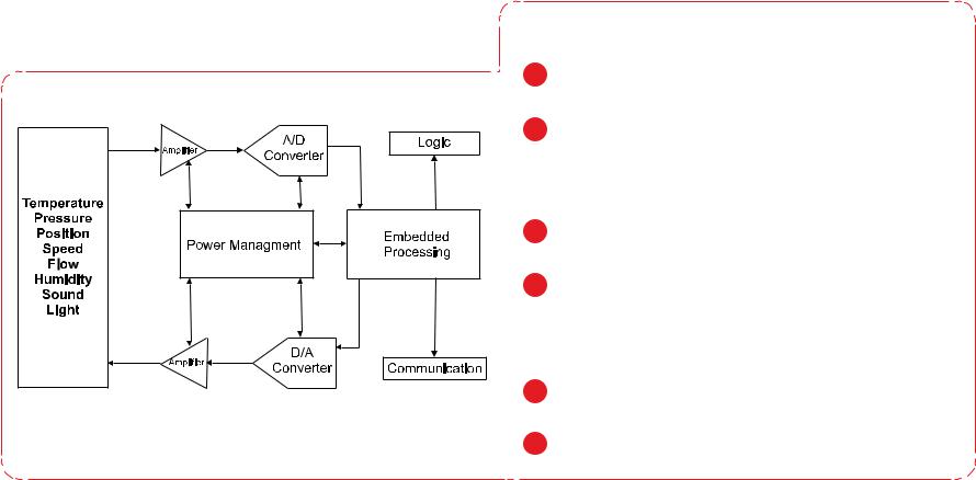
Although digital signal processing is the most common form of processing signals, analog signal processing cannot be completely avoided since the real world is analog in nature. Consider a typical signal chain (Figure below).
Figure: Signal Chain in an Electronic System
Typical signal chain
1A sensor converts the real-world signal into an analog electrical signal. This analog signal is often weak and noisy.
2Amplifiers are needed to strengthen the signal. Analog filtering may be necessary to remove noise from the signal. This “front end” processing improves the signal-to-noise ratio. Three of the most important building blocks used in this stage are (a) Operational Amplifiers, (b) Analog multipliers and (c) Analog Comparators.
3An analog-to-digital converter transforms the analog signal into a stream of 0s and 1s.
4The digital data is processed by a CPU, such as a DSP, a microprocessor, or a microcontroller. The choice of the processor depends on how intensive the computation is. A DSP may be necessary when realtime signal processing is needed and the computations are complex.
Microprocessors and microcontrollers may suffice in other applications.
5Digital-to-analog conversion (DAC) is necessary to convert the stream of 0s and 1s back into analog form.
6The output of the DAC has to be amplified before the analog signal can drive an external actuator.
It is evident that analog circuits play a crucial role in the implementation of an electronic system.
The goal of the Analog System Lab Course is to provide students an exposure to the fascinating world of analog and mixed-signal signal processing. The course can be adapted
page 10
for an undergraduate or a postgraduate curriculum. As part of the lab course, the student will build analog systems using analog ICs and study their macro models, characteristics and limitations. Our philosophy in designing this lab course has been to focus on system design rather than circuit design. We feel that many Analog Design classes
in the colleges focus on the circuit design aspect, ignoring the issues encountered in system design. In the real world, a system designer uses the analog ICs as building blocks. The focus of the system designer are to optimize system-level cost, power, and performance. IC manufacturers such as
Texas Instruments offer a large number
of choices of integrated circuits keeping in mind the diverse requirements of system designers. As a student, you must be aware of these diverse offerings of semiconductors and select the right IC for the right application. We have tried to emphasize this aspect in designing the experiments in this manual.
Analog System Lab Kit PRO 