

диафрагмированные волноводные фильтры / 2fb6bb1f-b73f-464b-bb4a-f78efd67023d
.pdfHome Search Collections Journals About Contact us My IOPscience
Graphene-based waveguide resonators for submillimeter-wave applications
This content has been downloaded from IOPscience. Please scroll down to see the full text. 2016 J. Phys. D: Appl. Phys. 49 325105 (http://iopscience.iop.org/0022-3727/49/32/325105)
View the table of contents for this issue, or go to the journal homepage for more
Download details:
IP Address: 128.243.46.132
This content was downloaded on 28/07/2016 at 15:11
Please note that terms and conditions apply.

|
|
Journal of Physics D: Applied Physics |
|
|
|
J. Phys. D: Appl. Phys. 49 (2016) 325105 (14pp) |
doi:10.1088/0022-3727/49/32/325105 |
|
Graphene-based waveguide resonators for submillimeter-wave applications
Andjelija Ž Ilić1, Branko Bukvić2, Milan M Ilić2,3 and Djuradj Budimir4
1 Institute of Physics, University of Belgrade, Pregrevica 118, 11080 Zemun-Belgrade, Serbia
2 School of Electrical Engineering, University of Belgrade, Bulevar Kralja Aleksandra 73, 11120 Belgrade, Serbia
3 ECE Department, Colorado State University, Fort Collins, CO, USA
4 Wireless Communications Research Group, University of Westminster, London W1W 6UW, UK
E-mail: andjelijailic@ieee.org
Received 12 March 2016, revised 22 May 2016
Accepted for publication 14 June 2016
Published 21 July 2016
Abstract
Utilization of graphene covered waveguide inserts to form tunable waveguide resonators is theoretically explained and rigorously investigated by means of full-wave numerical electromagnetic simulations. Instead of using graphene-based switching elements, the
concept we propose incorporates graphene sheets as parts of a resonator. Electrostatic tuning of the graphene surface conductivity leads to changes in the electromagnetic field boundary conditions at the resonator edges and surfaces, thus producing an effect similar to varying the electrical length of a resonator. The presented outline of the theoretical background serves to give phenomenological insight into the resonator behavior, but it can also be used to develop customized software tools for design and optimization of graphene-based resonators and filters. Due to the linear dependence of the imaginary part of the graphene surface impedance on frequency, the proposed concept was expected to become effective for frequencies above 100 GHz, which is confirmed by the numerical simulations. A frequency range from 100 GHz up to 1100 GHz, where the rectangular waveguides are used, is considered. Simple, all- graphene-based resonators are analyzed first, to assess the achievable tunability and to check the performance throughout the considered frequency range. Graphene–metal combined waveguide resonators are proposed in order to preserve the excellent quality factors typical for the type of waveguide discontinuities used. Dependence of resonator properties on key design parameters is studied in detail. Dependence of resonator properties throughout the frequency range of interest is studied using eight different waveguide sections appropriate for different frequency intervals. Proposed resonators are aimed at applications in the submillimeter-wave spectral region, serving as the compact tunable components for the design of bandpass filters and other devices.
Keywords: tunable circuits and devices, submillimeter-wave devices, graphene, boundary conditions, graphene–metal combined waveguide resonators
(Some figures may appear in colour only in the online journal)
1. Introduction
Millimeter and submillimeter wave regions of the electro magnetic (EM) spectrum are traditionally utilized in astrophysics, remote sensing, defense and security, as well as in biomedical imaging applications [1–4]. Recently, there has
been an increased interest in utilization of these frequencies in a range of commercial applications, including broadband communications, motivated mainly by the availability of large bandwidths required for the multigigabit short-range wireless communications [5]. Consequently, there is a constant advance in the development of components and systems for millimeter
0022-3727/16/325105+14$33.00 |
1 |
© 2016 IOP Publishing Ltd Printed in the UK |
J. Phys. D: Appl. Phys. 49 (2016) 325105 |
A Ž Ilić et al |
|
|
and submillimeter wave frequencies [6–8]. A major limiting factor hindering broader exploitation of this spectral region for some time is the shortage of efficient low-cost power sources. With the recent increased research efforts in this direction, more efficient power sources are to be devised [4]. Another difficulty to be resolved is the choice of appropriate materials for the design of devices and systems operating in this spectral region, i.e. at the boundary between microwaves and optics. Performance of PIN and varicap diodes, traditionally employed to obtain frequency reconfigurability and tunability, deteriorates with frequency. Micro electro-mechanical systems are used as an alternative; however, their switching speed is typically much lower and their power handling capability is low. Hence, there is a need to investigate alternative methods for attaining frequency tunability.
Graphene emerged, relatively recently, as a promising new material for photonics applications. In addition to its superior structural, mechanical and electrical properties, its electrically, magnetically and optically controllable conductivity makes it a good choice for the realization of tunable or reconfigurable components and devices. EM field interaction with graphene at terahertz frequencies has been successfully investigated for a variety of applications including plasmonic antennas, wave modulators, and terahertz lasers [9–15]. Possible utilization of this controllable conductivity in the millimeter and submillimeter wave range has yet to be addressed more thoroughly. The method for microwave and millimeter wave characterization of graphene surface impedance, presented in [16], has been illustrated by material characterization at X and Ka bands. The reactive component of surface impedance at these frequencies is not large enough to produce significant frequency tunability, regardless of the wave attenuation in graphene. Frequency independent surface inductivity, as well as the resistivity of graphene, leads to a linear increase of the reactive comp onent—versus the resistive impedance component ratio in the considered frequency range [17, 18]. We show here that reasonable tunability can be achieved for frequencies above 100 GHz using the electrostatic tuning.
Rectangular waveguides and rectangular waveguide resonators are an attractive solution for millimeter and submillimeter applications requiring large power handling capability along with reasonably low losses. An additional good property of rectangular waveguides is the fact that they have a wide bandwidth of operation within the monomode regime. Dimensions and corresponding frequency ranges for the commercially available waveguide sections [19, 20] operating at frequencies from about 100 GHz up to 1100 GHz are listed in table 1. A good five percent tunability has been achieved in our preliminary study [18] using graphene-based resonators, where the focus was on the 300 GHz frequency, which is currently investigated as a good candidate for employment in the multigigabit short-range wireless communications. This work presents a significant extension of [18], where we have presented only a proof of concept that the chosen method of attaining frequency tunability could be successfully employed at higher frequencies. We here start with the development of theoretical expressions for EM fields in the vicinity of the proposed waveguide discontinuities, which for the first time
give some physical insight into functioning principles of the suggested devices. Physics of graphene-based resonators is further illustrated in section 3, where an appropriately chosen example shows the impact on the EM boundary conditions and thus the field distribution of four distinct choices of the graphene stripe widths. The developed theoretical expressions are also applicable to other 2D materials that could be developed in the future. In addition, they can be directly embedded in the specialized filter design software. Moreover, the necessity to perform certain trade-offs among the design parameters, indicated in [18], is now thoroughly investigated. In addition to the illustrative examples showing the resonance curves, detailed numerical EM analyses of the dependence of the tunability range, insertion loss, and loaded quality factor on the graphene stripe width are performed, systematically varying the width of the graphene stripe from nonexistent to completely covering the E-plane insert in steps of 2.5% of the insert length. Finally, the dependence of graphene-based waveguide resonator properties on the frequency is investigated.
We propose and investigate here applications of graphene in waveguide resonators in the spectral region from 100 to 1100 GHz. For the proposed applications we present the theoretical background and thorough numerical validations using rigorous full-wave computational simulations based on the method of moments (MoM), and the finite element method (FEM) algorithms. In analyses we consider standard rectangular waveguide sections as canonical examples for invest igation of graphene efficiency in the considered frequency range, noting that graphene can be employed in the surface integrated waveguides and the hollow integrated waveguides as well. In particular, we study a single resonator, as a basic building block for millimeter and submillimeter wave filters.
An E-plane insert, considered in this study, is a waveguide discontinuity often employed in all-metal resonators and filters due to its simplicity and potential for accurate realization. Analytical expressions are initially derived to provide valuable insight into the underlying physical mechanisms of graphene-based resonator operation. However, equivalent analytical models of E-plane inserts exhibit nonlinear frequency dependence around the desired central frequency of operation. Hence, accurate analysis of E-plane inserts requires numer ical simulations or optimization algorithms [21]. Moreover, losses in graphene are higher than in the purely metallic parts of the surrounding resonator structure, hence mandating fullwave numerical computations of wave propagation. Detailed investigation of the proposed structure is conducted using the full-wave computational EM analysis tools based on the MoM and FEM, namely utilizing, respectively, the state-of-the-art commercial software packages WIPL-D [22] and HFSS [23].
2. Theoretical background
Standard rectangular waveguide section containing the resonator, which consists of two equally sized and symmetrically placed E-plane inserts, is shown in figure 1. The length of an E-plane insert, lT, is represented as lT = lM + lG to include the case where only a part of an insert (of length lG) is covered
2
J. Phys. D: Appl. Phys. 49 (2016) 325105 |
|
|
|
|
|
|
|
|
|
|
|
|
|
|
|
|
|
|
|
|
|
|
|
A Ž Ilić et al |
|||||||
|
|
|
|
|
|
|
|
|
|
|
|
|
|
|
|
|
|
|
|
|
|
|
|
|
|
|
|
|
|
|
|
|
|
|
|
Table 1. Rectangular metallic waveguides: frequency bands and waveguide dimensions. |
|
|
|
|
|
||||||||||||||||||||||
|
|
|
|
|
|
|
|
|
|
|
|
|
|
|
|
|
|
|
|
|
|
|
|
|
|
|
|
|
|
|
|
|
EIA designation/ |
IEEE |
Frequency |
|
|
Cut-off (TE10) |
Aperture |
Aperture |
|||||||||||||||||||||||
|
extended MIL [17] |
designation [16] |
range (GHz) |
|
|
frequency (GHz) |
width a (µm) |
height b (µm) |
|||||||||||||||||||||||
|
|
|
|
|
|
|
|
|
|
|
|
|
|
|
|
|
|
|
|
|
|
|
|
|
|
|
|
|
|
|
|
|
WR-10 |
WM-2540 |
75–110 |
59.01 |
|
|
|
|
|
|
2540.0 |
|
|
|
|
1270.0 |
|
||||||||||||||
|
WR-8 |
WM-2032 |
90–140 |
73.77 |
|
|
|
|
|
|
2032.0 |
|
|
|
|
1016.0 |
|
||||||||||||||
|
WR-6 |
WM-1651 |
110–170 |
90.79 |
|
|
|
|
|
|
1651.0 |
|
|
|
|
825.5 |
|
||||||||||||||
|
WR-5 |
WM-1295 |
140–220 |
115.75 |
|
|
|
|
|
|
1295.0 |
|
|
|
|
647.5 |
|
||||||||||||||
|
WR-4 |
WM-1092 |
170–260 |
137.27 |
|
|
|
|
|
|
1092.0 |
|
|
|
|
546.0 |
|
||||||||||||||
|
WR-3 |
WM-864 |
220–330 |
173.49 |
|
|
|
|
|
|
864.0 |
|
|
|
|
432.0 |
|
||||||||||||||
|
WR-2.8 |
WM-710 |
265–400 |
211.12 |
|
|
|
|
|
|
710.0 |
|
|
|
|
355.0 |
|
||||||||||||||
|
WR-2.2 |
WM-570 |
325–500 |
268.15 |
|
|
|
|
|
|
559.0 |
|
|
|
|
279.5 |
|
||||||||||||||
|
WR-1.9 |
WM-470 |
400–600 |
318.93 |
|
|
|
|
|
|
470.0 |
|
|
|
|
235.0 |
|
||||||||||||||
|
WR-1.5 |
WM-380 |
500–750 |
393.43 |
|
|
|
|
|
|
381.0 |
|
|
|
|
190.5 |
|
||||||||||||||
|
WR-1.2 |
WM-310 |
600–900 |
491.47 |
|
|
|
|
|
|
305.0 |
|
|
|
|
152.5 |
|
||||||||||||||
|
WR-1.0 |
WM-250 |
750–1100 |
590.15 |
|
|
|
|
|
|
254.0 |
|
|
|
|
127.0 |
|
||||||||||||||
|
|
|
|
|
|
|
|
|
|
|
|
|
|
|
|
|
|
|
|
|
|
|
|
|
|
|
|
|
|
|
|
|
|
|
|
|
|
|
|
|
|
|
|
|
|
|
|
|
|
|
|
|
|
|
|
|
|
|
|
|
|
|
|
|
|
|
|
|
|
|
|
|
|
|
|
|
|
|
|
|
|
|
|
|
|
|
|
|
|
|
|
|
|
|
|
|
|
|
|
|
|
|
|
|
|
|
|
|
|
|
|
|
|
|
|
|
|
|
|
|
|
|
|
|
|
|
|
|
|
|
|
|
|
|
|
|
|
|
|
|
|
|
|
|
|
|
|
|
|
|
|
|
|
|
|
|
|
|
|
|
|
|
|
|
|
|
|
|
|
|
|
|
|
|
|
|
|
|
|
|
|
|
|
|
|
|
|
|
|
|
|
|
|
|
|
|
|
|
|
|
|
|
|
|
|
|
|
|
|
|
|
|
|
|
|
|
|
|
|
|
|
|
|
|
|
|
|
|
|
|
|
|
|
|
|
|
|
|
|
|
|
|
|
|
|
|
|
|
|
|
|
|
|
|
|
|
|
|
|
|
|
|
|
|
|
|
|
|
|
|
|
|
|
|
|
|
|
|
|
|
|
|
|
|
|
|
|
|
|
|
|
|
|
|
|
|
|
|
|
|
|
|
|
|
|
|
|
|
|
|
|
|
|
|
|
|
|
|
|
|
|
|
|
|
|
|
|
|
|
|
|
|
|
|
|
|
|
|
|
|
|
|
|
|
|
|
|
|
|
|
|
|
|
|
|
|
|
|
|
|
|
|
|
|
|
|
|
|
|
|
|
|
|
|
|
|
|
|
|
|
|
|
|
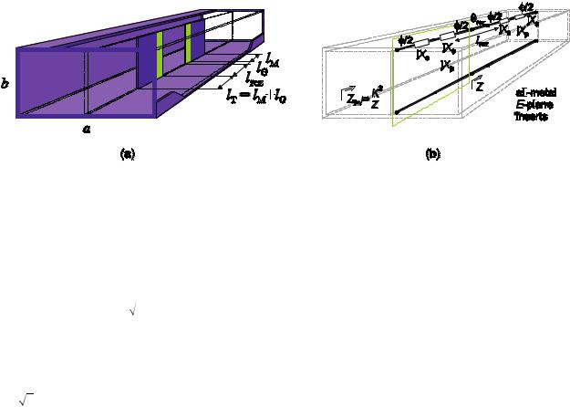
Figure 1. Waveguide resonator comprising two equal and symmetrically placed E-plane inserts: (a) the usual case of all-metal inductive inserts of the resonator, and (b) the normalized dominant mode equivalent circuit. When the resonator E-plane inserts consist of graphene layers, their surface impedance can be controlled via the bias voltage, influencing EM field distribution in the vicinity of waveguide discontinuities of total length lT. The resulting effects are similar to the effects of varying the effective resonator length by changing the distance, lrez, between the inserts. For the improved stop-band performance there should be the least difference in EM field distribution around the outer resonator edges, compared to the case of perfectly conducting inserts. This is addressed by applying graphene stripes, of length lG, only along the inner edges of the resonator E-plane inserts, whereas the remaining part of each insert, of length lM, is metallic.
by graphene. Propagation of the transverse electric (TE) and transverse magnetic (TM) modes is supported above the cutoff
frequency, given by fc,mn = ((m/a)2 + (n/b)2)/4εµ, with integer m and n. These modes can be derived from a magnetictype Hertzian potential and from an electric-type Hertzian potential, respectively [24]. Dominant mode of propagation is the TE10 mode, since a > b is usually considered. For stan-
dard |
waveguides a = 2b, so that fc,20 = fc,01 = 2fc,10 and |
fc, 11 |
= 5 fc, 10, allowing for as large as possible single-mode |
bandwidth from fc, 10 to 2fc, 10. Air filled waveguides are used in our analysis, with permittivity ε = ε0 and permeability
μ = μ0.
Waveguide discontinuities lead to the excitation of higher order evanescent modes, which vanish at a distance from the discontinuity planes; however, changes are introduced in the reflection from and transmission through the considered section. Due to similarity of waveguide modal field solutions and wave propagation along a transmission line, formally identical systems of equations can be written for the modal field solutions and transmission line voltage and current relations. Namely, each mode can be represented as an equivalent transmission line, thus a circuit representation of waveguide
discontinuities is possible. This is often utilized to facilitate analytical description of waveguide discontinuities.
2.1. All-metal E-plane resonators
Waveguide resonators and bandpass filters consisting of allmetal E-plane inserts were introduced as an answer to the need for an efficient, low cost, device, which can easily be mass -produced with desired accuracy [25]. Ever since, all-metal inserts remain appealing due to their small size and low losses.
Variational expression for the normalized admittance of an inductive insert is obtained according to [24], leading to the normalized dominant mode equivalent circuit of the discontinuity shown in figure 1(b). The equivalent symmetrical T-circuit of an E-plane insert can be symmetrically embedded in a length of a waveguide, incorporating the electrical length of φ/2 on each port. With the convenient choice of φ, equivalent T-circuit acts as an impedance inverter, or K-inverter, in a very narrow frequency range. In an idealized impedance inverter, impedance seen at one port, Z, appears at the other
port as Zinv = K2/Z. In the case of an E-plane insert, however, parameter K has nonlinear frequency dependence and
3

J. Phys. D: Appl. Phys. 49 (2016) 325105 |
A Ž Ilić et al |
|
|
can serve only as a first step approximation. Upon the calcul ation of equivalent circuit reactances Xs, Xp, normalized with respect to the waveguide characteristic impedance for the dominant mode, ZC, the electrical length φ is chosen as
φ = −arctan(2Xp + Xs) − arctan(Xs), |
(1) |
in order to approximate the equivalent circuit as a K-inverter defined by:
tan(2 arctan K) = |
2Xp |
|
. |
(2) |
|
1 + 2X X |
|
+ X2 |
|||
|
p |
s |
s |
|
|
The normalized reactances, Xs and Xp, are functions of the length, lT, of an E-plane insert. Frequency dependent para meters φ and K are in the first approximation calculated at some predefined ‘center’ frequency, f0. The electrical length θrez, corresponding to the distance between the two inserts, lrez, is then calculated taking into account the waveguide wavelength and subtracting the φ/2 electrical lengths of the two impedance inverters, in this case equal. In accordance with the resonator and filter synthesis using the half-wave prototypes, the resulting electrical length must be equal to π at the frequency f0:
θrez = lrez πa ε0µ0(2af0 )2 − 1 − φ = π. |
(3) |
Given Xs and Xp, the dimensions of a resonator can be approximately determined using (1)–(3).
To determine Xs and Xp, EM field in the vicinity of the insert of width g has to be represented as a sum of modal field solutions including the higher order modes, for the rectangular waveguide of width a and height b, on one side of the discontinuity plane, and for the two waveguides of width (a − g)/2 and height b, on the other side of the discontinuity plane. (Due to symmetry, only odd modes are required for the main waveguide.) A sufficient finite number of modes in an expansion has to be matched over the discontinuity plane, whereas the sum of field components at the metallic insert tends to zero (exactly
Figure 2. Waveguide discontinuity comprising a dielectric slab of finite length, lT, and thickness, d, and a layer of metallization or graphene of negligible thickness covering the dielectric slab side along the midline of the waveguide. The coordinate system shown is used in analytical expressions throughout the paper.
2.2. Dielectric slab with and without conductive layer
If a metallic E-plane insert, or any part of it, is to be replaced by graphene, a dielectric holder is needed as a support. Phase shifts of the guided wave, introduced by the dielectric slab, should be accounted for in the resonator design. In our case, dielectric slab of finite length, lT, is placed asymmetrically as shown in figure 2, so that a very thin layer of metallization or a graphene layer runs along the midline of the waveguide. An excellent example of analysis of asymmetrically placed dielectric slab, without the conductive layer, is given in [26] including the complete final expressions needed to numer ically calculate the scattering matrix. A very limited outline of the major derivation steps pertinent to the special case in figure 2 will be given next.
Since the discontinuity is uniform along the y-axis, higher order modes excited at the junction are the TEm0 modes. The appropriate x-component of the Hertzian vector potential for the considered case is
|
∞ |
|
|
|
|
|
|
|
|
|
|
|
|
|
|
|
|
|
|
|
|
|
|
|
|
|
|
|
|
|
|
|
|
∑ AIm sin(maπ x)e−jkIzmz, |
|
0 z |
lrez |
|
or z |
lrez |
|
+ lT , |
|
0 x a , |
(region I) |
|
|
||||||||||||||||||||
|
2 |
2 |
|
|
|||||||||||||||||||||||||||||
m=1 |
|
|
|
|
|
|
|
|
|
|
|
|
|
|
|
|
|
|
|
|
|
|
|
|
|
|
|
|
|
|
|
|
|
|
∞ |
|
|
|
|
|
|
|
|
|
|
|
|
|
|
|
|
|
|
|
|
|
|
|
|
|
|
|
|
|
|
|
|
|
∑(AIIm cos(kDxm x) + BIIm sin(kDxmx))e−jkzmz, |
lrez |
z |
lrez |
+ lT, |
|
a |
x |
a |
+ d, |
(region II) |
|
|||||||||||||||||||||
2 |
2 |
2 |
2 |
|
|
||||||||||||||||||||||||||||
Qx = m=1 |
|
|
|
|
|
|
|
|
|
|
|
|
|
|
|
|
|
|
|
|
|
|
|
|
|
|
|
|
|
|
|
|
|
|
∞ |
III |
A |
|
|
A |
|
A |
−jkzmz |
|
|
lrez |
|
lrez |
|
|
|
a |
|
|
(5) |
||||||||||||
|
∑ Am |
(−tan(kxma) cos(kxmx) + sin(kxmx))e |
|
|
|
, |
|
2 |
z |
2 |
+ lT, 2 + d x a, (region III) |
|
|||||||||||||||||||||
m=1 |
|
|
|
|
|
|
|
|
|
|
|
|
|
|
|
|
|
|
|
|
|
|
|
|
|
|
|
|
|
|
|
|
|
|
∞ |
IV |
A |
−jkzmz |
|
|
lrez |
|
lrez |
|
|
|
|
|
|
a |
|
|
|
|
|
|
|
|
|
|
|
||||||
|
∑ Am |
sin(kxm x)e |
|
, |
|
|
z |
|
|
+ lT, |
0 x |
|
|
, (region IV). |
|
|
|||||||||||||||||
|
|
|
2 |
2 |
2 |
|
|
||||||||||||||||||||||||||
m=1 |
|
|
|
|
|
|
|
|
|
|
|
|
|
|
|
|
|
|
|
|
|
|
|
|
|
|
|
|
|
|
|
|
|
equals zero for the perfect electric conductor (PEC)). For an accurate solution, computer aided calculations are required.
Alternatively, a commercial computer aided engineering (CAE) software tool can be used to determine the discontinuity scattering parameters, for different lengths of an insert in some predefined range of values. Equivalent T-circuit nor malized reactances are obtained from S-parameters as:
jX |
= |
1 + S11 |
− S21 |
, jX = |
2S21 |
. |
(4) |
|
|
|
|||||
s |
|
1 − S11 |
|
p |
(1 − S11)2 − S21 2 |
|
|
|
|
+ S21 |
|
|
|||
Three components of the EM field vanish, namely: Ex = 0, Hy = 0, Ez = 0. The nonzero components of the EM field are calculated using:
Ey = −jωµ |
∂Qx , |
Hx = ω2µ ε0εrQx + |
∂2Qx , |
Hz = |
∂2Qx . |
|
0 ∂z |
0 |
∂x2 |
|
∂x∂z |
|
|
|
|
|
(6) |
In the above, ω = 2πf is the angular frequency and εr is the relative permittivity, considered equal to unity everywhere
4

J. Phys. D: Appl. Phys. 49 (2016) 325105 |
A Ž Ilić et al |
|
|
except in region II, which is defined by (5) for the coordinate system given in figure 2. Equality of the tangential field components, Ey and Hz, at the region’s interfaces at x = a/2 and x = a/2 + d yields a system of linear equations. For a non-trivial solution, the system’s determinant has to vanish, leading to a transcendental equation for the transverse mode
propagation constants in air, kAxm, and in dielectric, kDxm:
D |
|
kDxm |
A a |
|
A |
|
|
a |
|
|
|
|
|
|||||
tan(kxmd) + |
|
|
(tan(kxm |
|
) + tan(kxm( |
|
− d))) |
|
|
|
|
|||||||
kAxm |
|
|
|
|
|
|||||||||||||
2 |
2 |
|
|
|
|
|||||||||||||
|
|
D 2 |
|
|
|
|
|
|
|
|
|
|
||||||
|
− |
kxm |
|
tan kD d |
) |
tan kA |
a |
|
) |
tan kA |
a |
− d |
)) |
= 0. |
||||
|
|
|
A |
( xm |
( xm |
2 |
|
( xm( |
2 |
|
|
|||||||
|
|
kxm |
|
|
|
|
|
|
|
|
|
|
|
|
(7) |
|||
|
|
|
|
|
|
|
|
|
|
|
|
|
|
|
|
|
|
|
Both kAxm and kDxm are expressed in terms of the longitudinal propagation factor kzm, which is equal for regions II, III, and IV, defined by (5) and figure 2. Equation (7) is numerically solved for kzm, further determining
kA |
2 = k 2 |
− k2 , |
kD |
2 = εrk 2 |
− k2 , |
k 2 |
= ω2µ ε0. |
(8) |
xm |
0 |
zm |
xm |
0 |
zm |
0 |
0 |
|
With respect to the longitudinal propagation factors of the
main waveguide, kIzm, obtained from kIzm2 = k20 −(mπ/a)2, amplitudes of the modal propagation constants, kzm, are larger,
implying shorter modal wavelengths. Considering the TE10 mode, the only one that can actually propagate in the main waveguide, the discontinuity section can be viewed as if it is filled with material of an equivalent dielectric constant εre,
given by εre = k−0 2(k2z1 + (π/a)2), reducing the phase velocity by a factor of εre . The phase shift introduced by the dielectric slab is approximately equal to
θD = lT |
|
kz1 |
|
− |
k20 − |
π 2 |
. |
|
|
|
|
||||||
|
|
|
|
|
|
(a ) |
|
(9) |
If the dielectric slab side at x = a/2 were covered with a negligibly thick PEC sheet (g 0 ), the boundary conditions would dictate the vanishing of the tangential field components, Ey and Hz, at both sides of the PEC sheet. This simplifies the field equations derived from the following x-component of the Hertzian potential:
using dependencies given in (8). For a metal of finite conductivity m, and permeability µ0, surface impedance of the
thin metal sheet can be calculated as ZS = (1+j) πfµ0 /σm. It corresponds to the ratio of the total tangential electric field component and total tangential magnetic field component at any point on a surface, i.e. ZS = Ey/Hz for a thin metallic sheet located at x = a/2. The attenuation is small and EM field distribution is almost identical to the PEC case.
2.3. Influence of the graphene surface conductivity
Surface conductivity of graphene, in the considered range of frequencies, stems solely from the intraband contributions. It is given by [17, 27]
|
2 |
|
|
|
|
µc |
|
σ(ω, µc, , T ) = |
−j qekBT |
|
|
µc |
+ 2 ln(e− |
|
+ 1) , |
|
kBT |
||||||
( |
) |
|
|||||
|
kBT |
|
|
|
|||
|
π 2 ω − j2 |
|
|
|
|||
|
|
|
|
|
(12) |
||
where ω is the angular frequency, µc is the chemical potential of graphene, represents the carrier scattering rate, T is the temperature, and kB the Boltzmann constant. The chemical potential, µc, kBT product, as well as the scattering rate,, are expressed in electronvolts, although in s−1 is used in (12). Elementary charge and the reduced Planck constant are denoted as qe and , respectively. Room temperature, T = 300 K, is assumed throughout the paper. The above equation is accurate at room temperature, in the millimeter and submillimeter wave frequency range where spatial-dispersion effects are negligible, provided that there is no magnetic field bias. The chemical potential, µc, depends on the level of chemical doping; however, it is also tunable using the relation between the chemical potential and the electrostatic bias field, Ebias [27]:
ε0π 2v2F |
Ebias = ∫ |
+∞ ϑ[(1 + e(ϑ−µc)/kBT)−1 − (1 + e(ϑ+µc)/kBT)−1]dϑ. |
|
q |
|||
0 |
|||
e |
|
(13) |
|
|
|
||
Electrostatic bias field, perpendicular to the graphene surface, is created by applying the bias voltage across the capacitor formed by the graphene layer and the gating electrode,
|
∞ |
|
|
|
|
|
|
|
|
|
|
|
|
|
|
|
|
|
|
|
|
|
|
|
|
|
|
|
|
|
|
|
|
|
|
|
|
∑ AIm sin(maπ x)e−jkIzmz, |
0 z |
lrez |
|
or z |
lrez |
+ lT, |
0 x a, (region I) |
|
|
|
|
|
|||||||||||||||||||||||||
2 |
2 |
|
|
|
|
|
|||||||||||||||||||||||||||||||
m=1 |
|
|
|
|
|
|
|
|
|
|
|
|
|
|
|
|
|
|
|
|
|
|
|
|
|
|
|
|
|
|
|
|
|
|
|
|
|
|
∞ |
|
|
|
|
|
|
|
|
|
|
|
|
|
|
|
|
|
|
|
|
|
|
|
|
|
|
|
|
|
|
|
|
|
|
|
|
|
∑ AIIm |
|
−tan(kDxm |
a |
) cos(kDxmx) + sin(kDxmx) e−jkzmz, |
|
lrez |
z |
lrez |
+ lT, |
|
a |
x |
a |
+ d, |
(region II) |
|
||||||||||||||||||||
|
|
|
|
|
|
|
|
|
|
|
|
|
|
||||||||||||||||||||||||
m=1 |
|
( |
2 |
|
|
|
|
|
) |
|
|
|
2 |
|
|
2 |
|
|
2 |
|
2 |
|
|
|
|||||||||||||
Qx = |
|
|
|
|
|
|
|
|
|
|
|
|
|
|
|
|
|
|
|
|
|
|
|
|
|
|
|
|
|
|
|
|
|
|
|
|
|
|
∞ |
III |
|
A |
A |
|
A |
−jkzmz |
|
lrez |
lrez |
a |
|
|
|
|
(10) |
||||||||||||||||||||
|
∑ Am |
|
(−tan(kxma) cos(kxmx) + sin(kxmx))e |
|
|
, |
|
|
|
|
z |
|
|
+ lT, |
|
|
|
+ d x a, |
(region III) |
|
|||||||||||||||||
|
|
|
|
2 |
|
2 |
2 |
|
|
|
|||||||||||||||||||||||||||
m∞=1 |
|
|
|
|
|
|
|
|
|
|
|
|
|
|
|
|
|
|
|
|
|
|
|
|
|
|
|
|
|
|
|
|
|
|
|
|
|
|
∑ AIVm |
sin(2maπ x)e−jkIVzmz, |
|
lrez |
z |
lrez |
+ lT, |
0 x |
a |
, (region IV). |
|
|
|
|
|
|
|
|
|
||||||||||||||||||
|
2 |
2 |
2 |
|
|
|
|
|
|
|
|
|
|||||||||||||||||||||||||
m=1 |
|
|
|
|
|
|
|
|
|
|
|
|
|
|
|
|
|
|
|
|
|
|
|
|
|
|
|
|
|
|
|
|
|
|
|
|
|
I 2 |
2 |
mπ |
2 |
and |
IV |
2 |
2 |
|
2 |
|||
In the above, kzm |
= k0 − |
( a ) |
|
kzm |
|
= k0 |
− (2mπ/a) , |
|||||
whereas kIIzm = kIIIzm = kzm is obtained from |
|
|
|
|
||||||||
tan(kDxmd) + |
kDxm |
tan(kAxm( |
a |
− d)) = 0, |
(11) |
|||||||
A |
||||||||||||
|
||||||||||||
|
|
|
|
2 |
|
|
|
|
|
|||
|
|
kxm |
|
|
|
|
|
|
|
|
|
|
separated by a thin dielectric layer. A metallic gating electrode in proximity to the graphene layer would affect the EM wave propagation; a metallic layer parallel to the graphene surface would itself present an E-plane insert, masking the effects of the tunable conductivity of graphene. Therefore, another graphene layer has to play the role of the gate electrode. Utilization
5

J. Phys. D: Appl. Phys. 49 (2016) 325105 |
|
|
|
|
|
|
|
|
|
|
|
|
|
|
|
|
|
|
|
|
|
|
|
|
|
|
|
|
|
A Ž Ilić et al |
||||||||||||||||
|
|
|
|
|
|
|
|
|
|
|
|
|
|
|
|
|
|
|
|
|
|
|
|
|
|
|
|
|
|
|
|
|
|
|
|
|
|
|
|
|
|
|
|
|
|
|
|
|
|
|
|
|
|
|
|
|
|
|
|
|
|
|
|
|
|
|
|
|
|
|
|
|
|
|
|
|
|
|
|
|
|
|
|
|
|
|
|
|
|
|
|
|
|
|
|
|
|
|
|
|
|
|
|
|
|
|
|
|
|
|
|
|
|
|
|
|
|
|
|
|
|
|
|
|
|
|
|
|
|
|
|
|
|
|
|
|
|
|
|
|
|
|
|
|
|
|
|
|
|
|
|
|
|
|
|
|
|
|
|
|
|
|
|
|
|
|
|
|
|
|
|
|
|
|
|
|
|
|
|
|
|
|
|
|
|
|
|
|
|
|
|
|
|
|
|
|
|
|
|
|
|
|
|
|
|
|
|
|
|
|
|
|
|
|
|
|
|
|
|
|
|
|
|
|
|
|
|
|
|
|
|
|
|
|
|
|
|
|
|
|
|
|
|
|
|
|
|
|
|
|
|
|
|
|
|
|
|
|
|
|
|
|
|
|
|
|
|
|
|
|
|
|
|
|
|
|
|
|
|
|
|
|
|
|
|
|
|
|
|
|
|
|
|
|
|
|
|
|
|
|
|
|
|
|
|
|
|
|
|
|
|
|
|
|
|
|
|
|
|
|
|
|
|
|
|
|
|
|
|
|
|
|
|
|
|
|
|
|
|
|
|
|
|
|
|
|
|
|
|
|
|
|
|
|
|
|
|
|
|
|
|
|
|
|
|
|
|
|
|
|
|
|
|
|
|
|
|
|
|
|
|
|
|
|
|
|
|
|
|
|
|
|
|
|
|
|
|
|
|
|
|
|
|
|
|
|
|
|
|
|
|
|
|
|
|
|
|
|
|
|
|
|
|
|
|
|
|
|
|
|
|
|
|
|
|
|
|
|
|
|
|
|
|
|
|
|
|
|
|
|
|
|
|
|
|
|
|
|
|
|
|
|
|
|
|
|
|
|
|
|
|
|
|
|
|
|
|
|
|
|
|
|
|
|
|
|
|
|
|
|
|
|
|
|
|
|
|
|
|
|
|
|
|
|
|
|
|
|
|
|
|
|
|
|
|
|
|
|
|
|
|
|
|
|
|
|
|
|
|
|
|
|
|
|
|
|
|
|
|
|
|
|
|
|
|
|
|
|
|
|
|
|
|
|
|
|
|
|
|
|
|
|
|
|
|
|
|
|
|
|
|
|
|
|
|
|
|
|
|
|
|
|
|
|
|
|
|
|
|
|
|
|
|
|
|
|
|
|
|
|
|
|
|
|
|
|
|
|
|
|
|
|
|
|
|
|
|
|
|
|
|
|
|
|
|
|
|
|
|
|
|
|
|
|
|
|
|
|
|
|
|
|
|
|
|
|
|
|
|
|
|
|
|
|
|
|
|
|
|
|
|
|
|
|
|
|
|
|
|
|
|
|
|
|
|
|
|
|
|
|
|
|
|
|
|
|
|
|
|
|
|
|
|
|
|
|
|
|
|
|
|
|
|
|
|
|
|
|
|
|
|
|
|
|
|
|
|
|
|
|
|
|
|
|
|
|
|
|
|
|
|
|
|
|
|
|
|
|
|
|
|
|
|
|
|
|
|
|
|
|
|
|
|
|
|
|
|
|
|
|
|
|
|
|
|
|
|
|
|
|
|
|
|
|
|
|
|
|
|
|
|
|
|
|
|
|
|
|
|
|
|
|
|
|
|
|
|
|
|
|
|
|
|
|
|
|
|
|
|
|
|
|
|
|
|
|
|
|
|
|
|
|
|
|
|
|
|
|
|
|
|
|
|
|
|
|
|
|
|
|
|
|
|
|
|
|
|
|
|
|
|
|
|
|
|
|
|
|
|
|
|
|
|
|
|
|
|
|
|
|
|
|
|
|
|
|
|
|
|
|
|
|
|
|
|
|
|
|
|
|
|
|
|
|
|
|
|
|
|
|
|
|
|
|
|
|
|
|
|
|
|
|
|
|
|
|
|
|
|
|
|
|
|
|
|
|
|
|
|
|
|
|
|
|
|
|
|
|
|
|
|
|
|
|
|
|
|
|
|
|
|
|
|
|
|
|
|
|
|
|
|
|
|
|
|
|
|
|
|
|
|
|
|
|
|
|
|
|
|
|
|
|
|
|
|
|
|
|
|
|
|
|
|
|
|
|
|
|
|
|
|
|
|
|
|
|
|
|
|
|
|
|
|
|
|
|
|
|
|
|
|
|
|
|
|
|
|
|
|
|
|
|
|
|
|
|
|
|
|
|
|
|
|
|
|
|
|
|
|
|
|
|
|
|
|
|
|
|
|
|
|
|
|
|
|
|
|
|
|
|
|
|
|
|
|
|
|
|
|
|
Figure 3. Effects on the resonator parameters of (a) the graphene surface inductance only, with Rg set to zero, (b) the realistic graphene surface impedance, and (c) the quartz support thickness. Standard WR-3 waveguide section with lrez = 360 µm, and lT = 280 µm
completely covered by the graphene layers, was analyzed. Scattering parameters for the all-metal case, with the f Mrez = 300.75 GHz, are
presented by the dash–dot–dot line in all graphs. In part (a), the dashed lines correspond to the 2D graphene sheet without a dielectric support revealing the tunability effect due to the graphene only, whereas the solid lines show the combined resonant frequency shifts and tunability due to the graphene-on-quartz. Additional phase shifts introduced by the dielectric slab are functions of the graphene surface inductance, resulting in a broader tunability range when the dielectric support is used. Different line colors (shades) in parts (a) and
(b) correspond to the graphene chemical potential values given in the legend. Scattering parameters accounting for the realistic loss in graphene-on-quartz resonators are shown in part (b). Results of an investigation into the effect of the quartz thickness on S-parameters are shown in part (c), through a comparison of S-parameters for two values of graphene chemical potential: 0.4 eV and 1.0 eV. Larger thickness yields a slightly broader tunability range, however at the expense of a larger shift between the reflected and the transmitted wave and somewhat worse quality factor (line colors/shades are explained in the legend). Therefore, the dielectric support should remain thin.
of such all-graphene gating and the graphene stacks, structures composed of two or more graphene layers separated by electrically thin dielectrics, has been theoretically investigated and experimentally verified [9, 12, 28–30]. Alumina, Al2O3, is often employed as the dielectric layer in-between the graphene sheets. We will assume a 100 nm thick Al2O3 layer, which is thick enough to neglect the quantum capacitance of graphene, but still sufficiently thin to allow for the low bias voltages of the graphene-based top gate. From the point of view of EM wave propagation, the described graphene stack is electrically very thin and the boundary conditions can be assumed constant throughout the graphene stack. Likewise, very small slits needed to connect the outer voltage generator to the two graphene layers are not deemed influential on the EM field distribution along the resonator edges nor the further EM wave propagation. Without the loss of generality, we will perform numerical EM modeling of the proposed structures, replacing the graphene stacks with single layers of negligible thickness exhibiting tunable surface conductivity. All of the results will be given for several chemical potentials in the range of interest, rather than for the corresponding bias volt ages, thus allowing for easier interpretation of results, once actual biasing conditions and the equivalent total stack conductivity are determined [29]. The Fermi velocity in graphene is vF ≈ 106 m s−1 and the chemical potential is easily tuned in the range (−1 eV, 1 eV). Graphene surface impedance,
Zg = Rg + jωLg, is obtained directly, with the surface resist ance and surface inductance given by
Rg = 2 |
qe |
|
Lg = |
|
|
π 2 |
|
|
Lg, |
|
|
|
. |
||
|
qe3kB T( |
µc |
+ 2 ln(e−µc/(kBT ) + 1)) |
||||
|
|
kBT |
|||||
|
|
|
(14) |
||||
The Boltzmann constant kB = 8.617 3325 × 10−5 eV K−1 and the reduced Planck constant = 1.054 571 726 × 10−34 Js are used, whereas µc is varied in the range (−1 eV, 1 eV).
If in the dielectric slab configuration shown in figure 2, the slab side located at x = a/2 is covered with a graphene layer, the EM field at this boundary surface will be significantly reduced compared with the pure dielectric slab. This effect is brought by the graphene conductivity, leading to the resonating effect when there are two conducting surfaces as in figure 1. Still, the EM field at x = a/2 will be far from zero, due to the finite, much larger than in the metallic case, real
part of the surface impedance, Rg πfµ0/σm, in the frequency range of interest. The real part of the surface impedance induces attenuation of the guided wave, whereas the imaginary, reactive component of the surface impedance is responsible for the resonant frequency shift. This is illustrated in figure 3, for the standard WR-3 waveguide section. High quality, low resistivity graphene, should be used to minimize losses.
6

J. Phys. D: Appl. Phys. 49 (2016) 325105 |
A Ž Ilić et al |
|
|
The appropriate x-component of the Hertzian vector potential is again given by (5). There is no need to introduce the new region at x = a/2, since the total tangential electric fields, Ey, can be considered constant at both sides and throughout the graphene layers belonging to the electrically thin conductive sheet. At the interface of regions II and III, where there are no free charges or currents, Ey, as well as Hz, have to be continuous over the interface. In order to satisfy the electric field boundary conditions at the graphene surface at x = a/2, and at x = a/2 + d boundary, we have to enforce the equality of the longitudinal propagation factor, kzm, for regions II, III, and IV. Resulting from the total Ey, the surface current density
of the graphene sheet equals JS = σEyι^y = Z−g 1Eyι^y. It is also related to the tangential magnetic fields at x = a/2, through JS = n × (HIVz − HIIz )ι^z, where n ≡ −ι^x represents the region IV surface normal. We thus develop the field components, Ey and Hz, in regions II, III, and IV using (6). Appropriate boundary conditions lead to the following system of equations:
in magnitude with varying longitudinal propagation factors. As a result, elements of the equivalent T-circuit in figure 1(b) become tunable. Changes in the equivalent circuit elements are reflected in the varying appropriate electrical length φ needed to obtain the function of the K-inverter element, further affecting the total electrical length of a resonator, θrez. In short, the tunable graphene surface impedance can be considered as a tunable effective length of the E-plane inserts, changing the length of a resonator, and thus leading to the change in its resonant frequency. As the modifications of resonator length are desired, there is no benefit in changing the overall length of the section comprising the two E-plane inserts, i.e. the allmetal inserts exhibit the best stop band performance. This led us to the proposal of the graphene–metal combined waveguide resonators, where an inner side of each E-plane insert adjacent to the resonator, lrez, is coated with graphene, whereas the rest of the inserts is purely metallic. With the aid of numerical simulations, different configurations will be analyzed and compared in the following sections.
|
cos(kDxm( |
a |
|
+ d)) |
sin(kDxm( |
a |
|
+ d)) |
|
sin(kAxm( 2a − d)) |
|
|||||||||||||
|
|
|
|
|
A |
|||||||||||||||||||
|
|
2 |
|
|
|
|
|
|
|
|
2 |
|
|
|
|
|
|
|
|
|
||||
|
|
|
|
|
|
|
|
|
|
|
|
|
|
|
|
|
|
|
|
|
|
cos(kxma) |
||
|
|
|
|
|
|
|
|
|
|
|
|
|
|
|
|
|
|
|
|
|
|
kAxm cos(kAxm( 2a − d)) |
||
|
D |
D |
a |
D |
D |
|
|
a |
||||||||||||||||
kxm sin(kxm( |
|
|
|
+ d)) |
−kxm cos(kxm( |
|
|
+ d)) |
|
|
||||||||||||||
2 |
2 |
|
A |
|||||||||||||||||||||
|
|
|
|
|
|
|
|
|
|
|
|
|
|
|
|
|
|
|
|
|
|
|
cos(kxma) |
|
|
|
|
D a |
|
|
D a |
|
|
|
|||||||||||||||
|
|
cos(kxm |
|
) |
|
|
sin(kxm |
|
) |
|
|
0 |
|
|||||||||||
|
2 |
|
2 |
|
||||||||||||||||||||
|
|
D |
D a |
|
D |
|
|
D a |
|
|
|
|||||||||||||
|
|
kxm sin(kxm |
|
) |
−kxm cos(kxm |
|
) |
0 |
|
|||||||||||||||
|
2 |
2 |
|
|||||||||||||||||||||
|
|
|
|
|
|
|
|
|
|
|
|
|
|
|
|
|
|
|
|
|
|
|
|
|
0
0
−sin(kAxm a2 )
jωµ0 sin(kA a ) + kA
Zg xm 2 xm
|
|
|
|
|
|
|
|
|
|
|
|
II |
|
0 |
|
|
|
|
|
|
|
|||||
|
|
|
AIIm |
|
|
|
|
|
|
|
Bm |
|
0 |
|
|||
|
|
Am |
|
|
|
|
|
|
|
|
|
III |
|
= |
0 |
. |
(15) |
|
|
AIVm |
|
0 |
|
|
||
A a |
|
|
|
|
|
|
|
|
cos(kxm |
|
) |
|
|
|
|
|
|
2 |
|
|
|
|
|
|
||
|
|
|
|
|
|
|
|
|
For a non-trivial solution, the system’s determinant has to vanish, yielding
|
D |
kDxm |
|
|
A a |
|
|
|
|
|
|
|
A |
a |
|
|
|
|
|
|||||||||
ξg tan(kxmd) + |
|
|
(tan(kxm |
|
) + ξg tan(kxm( |
|
|
− d))) |
|
|||||||||||||||||||
kAxm |
|
|
|
|||||||||||||||||||||||||
2 |
2 |
|
|
|||||||||||||||||||||||||
|
D 2 |
|
|
|
|
|
|
|
|
|
|
|
|
|
|
|
|
|
|
|
|
|
|
|
|
|
|
|
− |
kxm |
tan kD d |
) |
tan |
kA |
a |
) |
tan kA |
a |
− d |
)) |
= 0, |
|
|||||||||||||||
|
A |
( |
xm |
|
( |
|
xm |
2 |
|
|
( xm( |
2 |
|
|
|
|
|
(16a) |
||||||||||
kxm |
|
|
|
|
|
|
|
|
|
|
|
|
|
|
|
|
|
|
|
|
|
|
|
|
|
|||
|
ξg = 1 |
+ |
|
|
jωµ0 |
tan (kAxm |
a |
), |
|
|
|
|
|
|
|
|
|
|
|
|||||||||
|
|
|
|
A |
|
|
|
|
|
|
|
|
|
|||||||||||||||
|
|
|
|
|
|
|
|
|
|
|
|
|
|
|||||||||||||||
|
|
|
|
|
|
|
|
|
|
|
|
|
2 |
|
|
|
|
|
|
|
|
|
|
|
|
|||
|
|
|
|
|
Zgkxm |
|
|
|
|
|
|
|
|
|
|
|
|
|
|
|
|
|
|
|
|
|||
|
|
|
|
|
ω2Lgµ a + jωRgµ a tan (kAxm |
a |
) |
|
|
|||||||||||||||||||
|
|
|
|
|
|
|
||||||||||||||||||||||
|
ξ = 1 |
+ |
|
|
|
|
|
0 |
|
|
|
|
|
0 |
|
|
|
|
|
|
2 |
. |
(16b) |
|||||
|
|
|
|
|
|
|
|
|
|
|
|
|
|
|
|
|
|
|
|
|
|
|||||||
|
g |
|
|
|
|
2(Rg2 + ω2 Lg2) |
kAxma/2 |
|
|
|
||||||||||||||||||
|
|
|
|
|
|
|
|
|
|
|||||||||||||||||||
In the limit Zg 0, we have to multiply the equation (16a) with Zg. The only remaining non-zero terms result in
IV a |
( |
D |
|
kDxm |
A |
|
a |
) |
|
|||
(sin kxm |
|
) |
tan(kxmd) + |
|
tan(kxm( |
|
− d)) = 0, |
leading to |
||||
2 |
kAxm |
2 |
||||||||||
equations |
|
(10) and |
(11). |
In the |
limit Zg ∞, |
we obtain |
||||||
ξg ≡ 1, and (16a) reduces to equation (7), describing the purely dielectric slab.
In between the two limits, Zg modifies the EM fields significantly, depending on intrinsic material properties, frequency, and the applied bias field. With a change in Zg, evanescent higher order modes of the coated surface at x = a/2 decrease
2.4. Full-wave EM analysis
The numerical simulations assume quartz as a support for graphene layers and a thin film metallization. This choice has been motivated by two reasons. Firstly, fused silica quartz is an excellent substrate for the millimeter and submillimeter wave applications due to the relatively low dielectric constant and a small loss tangent. Secondly, quartz is a substrate material highly compatible with graphene. In addition to very usual wet-etching techniques for the transfer of graphene films grown on another substrate [31], there are also many recent techniques for direct generation of graphene on quartz, e.g. laser-based direct synthesis [32]. Reasonable adhesion of metallic thin films, copper (Cu) and gold (Au), on quartz, requires somewhat more complicated deposition techniques. Thin film metallization on quartz is usually comprised of two layers, the first one being a strongly oxidized metal such as chromium or titanium [33, 34]. The quartz dielectric constant and loss tangent equal εr = 3.78 and tan δ = 0.000 228, respectively. Quartz substrate thickness for the WR-3 waveguide is chosen as the commercially available 50 µm. For consistency, the ratio of quartz support thickness and the waveguide broad wall is kept equal to d /a = 1/16 for all considered waveguide sections, given in table 1. Close to 1 THz, a different material might be a better choice. In that case, phase shift and loss could differ with the same qualitative behavior of resonators.
7

J. Phys. D: Appl. Phys. 49 (2016) 325105 |
|
|
|
|
|
|
|
|
|
|
|
|
|
|
|
|
|
|
|
|
A Ž Ilić et al |
||||||||||||||||||||||
|
|
|
|
|
|
|
|
|
|
|
|
|
|
|
|
|
|
|
|
|
|
|
|
|
|
|
|
|
|
|
|
|
|
|
|
|
|
|
|
|
|
|
|
|
|
|
|
|
|
|
|
|
|
|
|
|
|
|
|
|
|
|
|
|
|
|
|
|
|
|
|
|
|
|
|
|
|
|
|
|
|
|
|
|
|
|
|
|
|
|
|
|
|
|
|
|
|
|
|
|
|
|
|
|
|
|
|
|
|
|
|
|
|
|
|
|
|
|
|
|
|
|
|
|
|
|
|
|
|
|
|
|
|
|
|
|
|
|
|
|
|
|
|
|
|
|
|
|
|
|
|
|
|
|
|
|
|
|
|
|
|
|
|
|
|
|
|
|
|
|
|
|
|
|
|
|
|
|
|
|
|
|
|
|
|
|
|
|
|
|
|
|
|
|
|
|
|
|
|
|
|
|
|
|
|
|
|
|
|
|
|
|
|
|
|
|
|
|
|
|
|
|
|
|
|
|
|
|
|
|
|
|
|
|
|
|
|
|
|
|
|
|
|
|
|
|
|
|
|
|
|
|
|
|
|
|
|
|
|
|
|
|
|
|
|
|
|
|
|
|
|
|
|
|
|
|
|
|
|
|
|
|
|
|
|
|
|
|
|
|
|
|
|
|
|
|
|
|
|
|
|
|
|
|
|
|
|
|
|
|
|
|
|
|
|
|
|
|
|
|
|
|
|
|
|
|
|
|
|
|
|
|
|
|
|
|
|
|
|
|
|
|
|
|
|
|
|
|
|
|
|
|
|
|
|
|
|
|
|
|
|
|
|
|
|
|
|
|
|
|
|
|
|
|
|
|
|
|
|
|
|
|
|
|
|
|
|
|
|
|
|
|
|
|
|
|
|
|
|
|
|
|
|
|
|
|
|
|
|
|
|
|
|
|
|
|
|
|
|
|
|
|
|
|
|
|
|
|
|
|
|
|
|
|
|
|
|
|
|
|
|
|
|
|
|
|
|
|
|
|
|
|
|
|
|
|
|
|
|
|
|
|
|
|
|
|
|
|
|
|
|
|
|
|
|
|
|
|
|
|
|
|
|
|
|
|
|
|
|
|
|
|
|
|
|
|
|
|
|
|
|
|
|
|
|
|
|
|
|
|
|
|
|
|
|
|
|
|
|
|
|
|
|
|
|
|
|
|
|
|
|
|
|
|
|
|
|
|
|
|
|
|
|
|
|
|
|
|
|
|
|
|
|
|
|
|
|
|
|
|
|
|
|
|
|
|
|
|
|
|
|
|
|
|
|
|
|
|
|
|
|
|
|
|
|
|
|
|
|
|
|
|
|
|
|
|
|
|
|
|
|
|
|
|
|
|
|
|
|
|
|
|
|
|
|
|
|
|
|
|
|
|
|
|
|
|
|
|
|
|
|
|
|
|
|
|
|
|
|
|
|
|
|
|
|
|
|
|
|
|
|
|
|
|
|
|
|
|
|
|
|
|
|
|
|
|
|
|
|
|
|
|
|
|
|
|
|
|
|
|
|
|
|
|
|
|
|
|
|
|
|
|
|
|
|
|
|
|
|
|
|
|
|
Figure 4. Dependence of the resonator S-parameters on the relaxation time of charge carriers, τ. Results are presented for the standard WR- 2.2 waveguide section with lrez = lT = 210 µm, with lT completely covered by the graphene layers (line colors/shades are explained in the
legend). The S-parameters corresponding to the all-metal resonator are given for comparison by the dash–dot–dot line ( f Mrez 478 GHz). Results are shown for two values of the graphene chemical potential: 0.4 eV and 1.0 eV. There is no impact of the carrier relaxation time on
the tunability range. However, the observed increase in the insertion loss makes the concept impractical for low quality graphene layers.
In the analyses of the graphene–metal combined waveguide resonators we assume a thin film metallization of Cu for the WR-6, WR-4 and WR-3 waveguide sections, and a thin film metallization of Au in all other cases. The skin effect has been modeled accordingly, taking the DC conductivities of Cu and Au, σCu = 58.0 MS m−1 and σAu = 41.0 MS m−1, respectively. It has been shown previously, that the losses in graphene stripe were dominant in comparison with metallization as well as dielectric loss [18]; therefore, the effects of the metallization surface roughness were not considered here.
As mentioned above, the surface conductivity of graphene at room temperature, for a given frequency, depends on the chemical potential of graphene, µc, and the carrier scattering rate, . The chemical potential, related to the level of chemical doping and the applied electrostatic bias field, is easily tuned in the range (−1 eV, 1 eV), with the ±(0.2 eV, 1.0 eV) interval of interest in this study. This choice of working interval corresponds to the concentration of charge carriers that is already somewhat increased, either by the chemical doping, or by the initially applied bias voltage. Further biasing allows for the precise control of the chemical potential, and thus the attained low resistivity, as the chemical potential variation with bias voltage in this interval is less steep than at zero chemical potential. Additionally, the relation between the chemical potential and the electrostatic bias field is more linear, as shown in figure 3 in [27]. The phenomenological scattering rate, , is related to the relaxation time of charge carriers, τ = (2 )−1, which can differ significantly in the cases of intrinsic and doped graphene [35]. Carrier relaxation time at subterahertz frequencies can be identified with the DC relaxation time, τ ≈ τDC = µ nc π /(qevF), which arises mainly from impurities [36]. DC relaxation time is directly proportional to the charge carrier mobility, µ, and the square root of the carrier concentration, nc. Experimental investigation of high-purity graphene, found in nature on the surface of bulk graphite, sets the low temperature scattering time limit at τ ≈ 20 ps [35]. High mobility of charge carriers has also been obtained in the case of the suspended graphene [37, 38], up to μ = 200 000 cm2 V−1 s−1 at low temper atures and μ = 120 000 cm2 V−1 s−1 near room temperature.
Influence of substrate type and quality on carrier mobility can be significant. In a study utilizing the Monte Carlo method to investigate the substrate influence on the carrier mobility for three different substrates [39], high charge carrier mobility was obtained only for the hexagonal boron nitride (h-BN) substrate (μ ≈ 170 000 cm2 V−1 s−1. That finding is in accordance with the experimental results [40]. High carrier mobility has been observed for the multiple-graphene-layer (MGL) structures grown epitaxially on SiC, as well [14, 41–44]. Growth on the Si-face of SiC results in a lower mobility few-layer graphene, whereas growth on the C-face results in a high mobility multilayer graphene (μ ≈ 200 000 cm2 V−1 s−1). The number and mobility of graphene layers can thus be controlled by controlling the crystal orientation of the SiC. Once fabricated, such MGL structures can be transferred to a different substrate [44]. The real part of the intraband graphene conductivity always contributes as a loss. Since introducing large losses is highly undesirable in the waveguiding applications, high-quality low-loss graphene should be used. Therefore, the moderately long relaxation time, τ = 3 ps, is considered in the numerical examples. The impact of the carrier relaxation time on tunability and insertion loss of the proposed waveguide resonators is illustrated in figure 4.
The tunability effect achieved by the utilization of the adjustable graphene surface impedance in resonators comprised of E-plane inserts stems from the adjustment of the boundary conditions, as described by equations (16a) and (16b). Numerical analysis of a resonator using the WR-3 waveguide section is performed first, to qualitatively illustrate the effects on the resonator parameters of the real and imaginary parts of the surface impedance as well as the dielectric support thickness. As listed in table 2, the resonator length and the E-plane
insert length were chosen as lrez = 360 µm and lT = 280 µm, respectively. The results are shown in figure 3. For this first
resonator, all-graphene E-plane inserts were considered, i.e. the quartz support of the total length lT was assumed to be covered completely by the graphene. Simulations confirm the dependence of the obtained tunability range on the graphene surface inductance, both with Rg =0 and Rg ≠0. The real part of the graphene surface impedance contributes as a loss, on
8

J. Phys. D: Appl. Phys. 49 (2016) 325105 |
A Ž Ilić et al |
|
|
Table 2. Graphene-on-quartz waveguide resonators: considered dimensions and resonant frequencies.
EIA/Ext. MIL |
|
|
lrez (µm) |
lT (µm) |
|
f Mrez (GHz) |
|
|
f 0.2rez eV (GHz) |
|
|
f 0.4rez eV (GHz) |
|
|
f 1.0rezeV (GHz) |
|||||||||||||||||||||||||||||||||||||||||||
WR-6 |
720.0 |
|
|
|
535.3 |
|
|
|
|
|
|
155.00 |
143.00 |
|
|
|
|
|
147.50 |
|
|
|
|
|
|
|
151.25 |
|
|
|
|
|
||||||||||||||||||||||||||
WR-4 |
420.0 |
|
|
|
354.1 |
|
|
|
|
|
|
244.00 |
216.00 |
|
|
|
|
|
226.50 |
|
|
|
|
|
|
|
235.25 |
|
|
|
|
|
||||||||||||||||||||||||||
WR-3 |
360.0 |
|
|
|
280.0 |
|
|
|
|
|
|
300.75 |
262.00 |
|
|
|
|
|
276.00 |
|
|
|
|
|
|
|
288.50 |
|
|
|
|
|
||||||||||||||||||||||||||
WR-2.8 |
260.0 |
|
|
|
230.6 |
|
|
|
|
|
|
380.25 |
320.50 |
|
|
|
|
|
341.00 |
|
|
|
|
|
|
|
360.50 |
|
|
|
|
|
||||||||||||||||||||||||||
WR-2.2 |
210.0 |
|
|
|
181.2 |
|
|
|
|
|
|
479.50 |
393.75 |
|
|
|
|
|
421.25 |
|
|
|
|
|
|
|
449.50 |
|
|
|
|
|
||||||||||||||||||||||||||
WR-1.5 |
146.0 |
|
|
|
123.5 |
|
|
|
|
|
|
700.25 |
549.50 |
|
|
|
|
|
590.00 |
|
|
|
|
|
|
|
640.25 |
|
|
|
|
|
||||||||||||||||||||||||||
WR-1.2 |
132.0 |
|
|
|
98.8 |
|
|
|
|
|
|
840.50 |
656.00 |
|
|
|
|
|
700.00 |
|
|
|
|
|
|
|
762.00 |
|
|
|
|
|
||||||||||||||||||||||||||
WR-1.0 |
104.0 |
|
|
|
82.4 |
|
|
|
|
|
|
1029.50 |
786.50 |
|
|
|
|
|
835.00 |
|
|
|
|
|
|
|
915.50 |
|
|
|
|
|
||||||||||||||||||||||||||
|
|
|
|
|
|
|
|
|
|
|
|
|
|
|
|
|
|
|
|
|
|
|
|
|
|
|
|
|
|
|
|
|
|
|
|
|
|
|
|
|
|
|
|
|
|
|
|
|
|
|
|
|
|
|
|
|
|
|
|
|
|
|
|
|
|
|
|
|
|
|
|
|
|
|
|
|
|
|
|
|
|
|
|
|
|
|
|
|
|
|
|
|
|
|
|
|
|
|
|
|
|
|
|
|
|
|
|
|
|
|
|
|
|
|
|
|
|
|
|
|
|
|
|
|
|
|
|
|
|
|
|
|
|
|
|
|
|
|
|
|
|
|
|
|
|
|
|
|
|
|
|
|
|
|
|
|
|
|
|
|
|
|
|
|
|
|
|
|
|
|
|
|
|
|
|
|
|
|
|
|
|
|
|
|
|
|
|
|
|
|
|
|
|
|
|
|
|
|
|
|
|
|
|
|
|
|
|
|
|
|
|
|
|
|
|
|
|
|
|
|
|
|
|
|
|
|
|
|
|
|
|
|
|
|
|
|
|
|
|
|
|
|
|
|
|
|
|
|
|
|
|
|
|
|
|
|
|
|
|
|
|
|
|
|
|
|
|
|
|
|
|
|
|
|
|
|
|
|
|
|
|
|
|
|
|
|
|
|
|
|
|
|
|
|
|
|
|
|
|
|
|
|
|
|
|
|
|
|
|
|
|
|
|
|
|
|
|
|
|
|
|
|
|
|
|
|
|
|
|
|
|
|
|
|
|
|
|
|
|
|
|
|
|
|
|
|
|
|
|
|
|
|
|
|
|
|
|
|
|
|
|
|
|
|
|
|
|
|
|
|
|
|
|
|
|
|
|
|
|
|
|
|
|
|
|
|
|
|
|
|
|
|
|
|
|
|
|
|
|
|
|
|
|
|
|
|
|
|
|
|
|
|
|
|
|
|
|
|
|
|
|
|
|
|
|
|
|
|
|
|
|
|
|
|
|
|
|
|
|
|
|
|
|
|
|
|
|
|
|
|
|
|
|
|
|
|
|
|
|
|
|
|
|
|
|
|
|
|
|
|
|
|
|
|
|
|
|
|
|
|
|
|
|
|
|
|
|
|
|
|
|
|
|
|
|
|
|
|
|
|
|
|
|
|
|
|
|
|
|
|
|
|
|
|
|
|
|
|
|
|
|
|
|
|
|
|
|
|
|
|
|
|
|
|
|
|
|
|
|
|
|
|
|
|
|
|
|
|
|
|
|
|
|
|
|
|
|
|
|
|
|
|
|
|
|
|
|
|
|
|
|
|
|
|
|
|
|
|
|
|
|
|
|
|
|
|
|
|
|
|
|
|
|
|
|
|
|
|
|
|
|
|
|
|
|
|
|
|
|
|
|
|
|
|
|
|
|
|
|
|
|
|
|
|
|
|
|
|
|
|
|
|
|
|
|
|
|
|
|
|
|
|
|
|
|
|
|
|
|
|
|
|
|
|
|
|
|
|
|
|
|
|
|
|
|
|
|
|
|
|
|
|
|
|
|
|
|
|
|
|
|
|
|
|
|
|
|
|
|
|
|
|
|
|
|
|
|
|
|
|
|
|
|
|
|
|
|
|
|
|
|
|
|
|
|
|
|
|
|
|
|
|
|
|
|
|
|
|
|
|
|
|
|
|
|
|
|
|
|
|
|
|
|
|
|
|
|
|
|
|
|
|
|
|
|
|
|
|
|
|
|
|
|
|
|
|
|
|
|
|
|
|
|
|
|
|
|
|
|
|
|
|
|
|
|
|
|
|
|
|
|
|
|
|
|
|
|
|
|
|
|
|
|
|
|
|
|
|
|
|
|
|
|
|
|
|
|
|
|
|
|
|
|
|
|
|
|
|
|
|
|
|
|
|
|
|
|
|
|
|
|
|
|
|
|
|
|
|
|
|
|
|
|
|
|
|
|
|
|
|
|
|
|
|
|
|
|
|
|
|
|
|
|
|
|
|
|
|
|
|
|
|
|
|
|
|
|
|
|
|
|
|
|
|
|
|
|
|
|
|
|
|
|
|
|
|
|
|
|
|
|
|
|
|
|
|
|
|
|
|
|
|
|
|
|
|
|
|
|
|
|
|
|
|
|
|
|
|
|
|
|
|
|
|
|
|
|
|
|
|
|
|
|
|
|
|
|
|
|
|
|
|
|
|
|
|
|
|
|
|
|
|
|
|
|
|
|
|
|
|
|
|
|
|
|
|
|
|
|
|
|
|
|
|
|
|
|
|
|
|
|
|
Figure 5. Tunability and loss analysis for the graphene-on-quartz waveguide resonators. (a) Realistic values for the tunability range (Rg ≠0) are denoted as ‘quartz’. Theoretical maxima obtained assuming the lossless graphene are denoted as ‘maximal’ (for the chosen length of the E-plane inserts). (b) Insertion loss: mean value, maximum and minimum, for the graphene chemical potential varied in the
range from 0.2 to 1.0 eV. Frequency points are determined by the f Mrez for the considered waveguide section.
the order of 3 dB for the considered case. Lower mobility graphene sheets have the same dependence of the graphene surface inductance on the chemical potential; therefore, the tunability range remains the same, regardless of the carrier relaxation time. Insertion loss, on the other hand, increases, which suggests that the low quality graphene is not appropriate for the considered resonator type. This has been illustrated by the results shown in figure 4, corresponding to several values of the carrier relaxation time, τ, and the WR-2.2 waveguide
section with lrez = lT = 210 µm. A slightly broader tunability range with the increase in dielectric slab thickness, as
seen from figure 3, does not compensate for the deteriorated quality factor and the larger frequency mismatch between the reflected and the transmitted wave; therefore, it should remain thin. With the above considerations in mind, we proceed with analyses of a total of eight waveguides chosen from table 1.
3. Results and discussion
We analyze the graphene-based waveguide resonators corresp onding to the WR-6, WR-4, WR-3, WR-2.8, WR-2.2, WR-1.5, WR-1.2, and WR-1.0 waveguide sections listed in table 1. It is of interest to confirm the validity of the proposed concept throughout the frequency range from 100 to 1100 GHz, and to check for the expected frequency dependence of the obtained tunability and loss. For each of the eight considered waveguides, resonator length is chosen so that the all-metal
resonant frequency, f Mrez, falls into the upper portion of the useful frequency range. Under the influence of the graphene surface impedance, the resonant frequency is shifted toward the lower end of the frequency range. To make different waveguide resonators comparable, the E-plane insert length is kept at a multiple of the waveguide broad wall a, in all analyzed cases. For the graphene-on-quartz resonators, where the complete length of an insert is covered by graphene, lT = 0.324a was considered. Similarly, in all simulations, the quartz thickness is a multiple of the waveguide broad wall, d = a/16. The results are summarized in table 2 and figure 5. The same eight values of the graphene chemical potential used in figure 3 were also utilized for the S-parameter calculation for each of the waveguide sections analyzed and presented in figure 5.
Results shown in figure 5 reveal the increase of the tunability range with frequency, with the obtained tunability percentage above 12% at higher frequencies, for the given insert length of lT = 0.324a. Resonant frequencies for the all-metal resonators, for the two values of graphene chemical potential corresponding to the limits of the considered tunability range, as well as the resonant frequency for µc = 0.4 eV, located close to the center of the tunability range, are listed in table 2. As can be seen in figure 5, insertion loss decreases with frequency, which, along with the increase of tunability, makes the concept of graphene-based waveguide resonators appealing for the considered frequency range. However, as can be observed from figure 3(b), and this is similar for all
9