

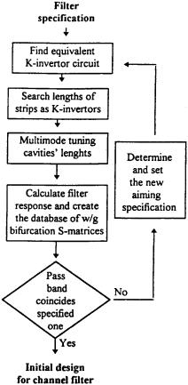
Figure 2. Flow chart for filter synthesis scheme.
In the next step, the band edge frequencies of the filter are corrected by compensating for the frequency dispersion of the septa and the phase velocity. This is done in the following way. Let the desired cut-off frequencies of the filter be fb and
fc. Let the corresponding analyzed cut-off fre- |
|||
quencies after |
the first analysis be |
fbX and |
fcX. |
Therefore, we |
obtain the corrections D fb c. s |
||
fb c. y fbX c.. Using this correction factor, we |
set |
||
our new input |
cut-off frequencies |
fb c. new. s |
|
D fb c. old. q D fb c.. With these new values of the input frequencies we enter the K-inverter stage of the filter synthesis. The iteration process is repeated until the desired passband is realized. Not more than four iterations are needed to achieve the desired cut-off frequencies, within 1%, even in the upper part of the waveguide operating frequency range. Also, each iteration of tuning does not require recalculation of the S- matrices of bifurcated junction discontinuities. The database generated for the bifurcated junction in the first iteration is used in subsequent iterations.
CAD of Wa¨eguide E-Plane Diplexers 107
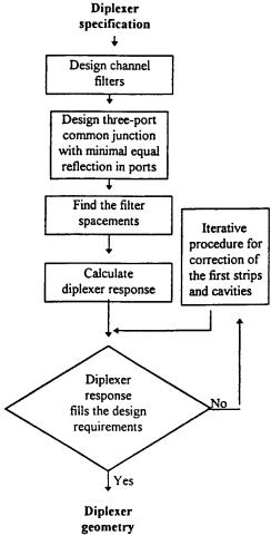
V. DIPLEXER DESIGN PROCEDURE BASED ON EQUIREFLECTION THREE-PORT JUNCTION
This procedure of diplexer design is based on matching two arms of a three-port junction by positioning an ideal reflector in the third arm. Let us assume that the symmetric three-port junction has the dominant mode S-matrix S11i j. and i, j are the arm numbers. If
<S1112. < s <S1113. <, |
1. |
if |
|
<S1111. < s <S1122. <, |
2. |
then by moving the perfect reflector in the third arm, it is possible to obtain a full matching of the first and the second arms. The condition for existence of such a matching is given by
2g l q arg R11 q arg |
S1111.S1133. y S1113.S1131. |
/ |
S1111. |
||
s 2 np , |
n s 0, 1, 2, . . . , |
3. |
where g is the propagation constant of the dominant mode in the third arm, l is the distance between the reference plane of the three-port junction and the reflector in the third arm, and R11 is the reflection coefficient of the reflector. Considering a band pass filter outside its passband as a reflector and positioning it according to eq. 3., one can match the common junction at the center frequency of the other filter. Therefore, if the following conditions are fulfilled at the center frequencies f01 and f02 of the channel filters:
<S1111. < s <S1122. < fsf 01 , |
4. |
and |
|
<S1111. < s <S1133. < fsf 02 , |
5. |
then the desired characteristics of the diplexer can be obtained by placing the channel filters at appropriate distances from the common junction in arms 2 and 3. The flow chart for the above procedure is shown in Figure 3. Note that the searching for the exact locations of the filters from the corresponding reference planes of the common junction are not carried out by eq. 3.,
108 Kirilenko et al.
Figure 3. Flow chart for diplexer synthesis.
but by means of a numerical iterative procedure which takes into account the multimode interaction among the channel filters and the common junction, using eq. 3. as an initial approximation. Conditions given by eqs. 4. and 5. are not always provided for a given diplexer configuration. A simpler condition used for a symmetrical three-port junction, instead of 4. and 5., is
<S1111. < s <S1122. < s <S1133. < fsfc j , |
6. |
where f01 - fc j - f02 . Such a unit can be called a Y-type unit and we will call the corresponding
design approach the Y-scheme. Combining eq. 6. with the unitary property of the S-matrix requires
that <S11ii. < G 13 , i s 1, 2, 3; for the dominant mode. This inequality imposes a limiting factor on the
realizable bandwidths of the channel filters in the Y-scheme. The smaller the value of <S11ii. <, the wider is the frequency band over which the
common junction remains matched. Ideally, it is desirable that together with 6. we should have <S11ii. < s 13 over a band of frequencies that encompasses the passbands of both channels and the guard band between them. Equation 6. can be satisfied over the required band only approximately which gives an additional factor limiting the characteristics of the diplexer.
Dispersion of phase characteristics of the common junction influences the overall frequency response of the diplexer synthesized by the Y- scheme. Equation 3. shows that the matching of two arms of the common junction has a resonant nature. Since a weak resonant characteristic of the matched common junction is superimposed on the frequency responses of the filters, it leads to degradation of channel responses at the cut-off frequencies.
Having discussed the general properties of waveguide three-port junctions, let us turn our attention to an equireflection three-port common junction of a waveguide diplexer. Reference w16x used the simplest E-plane step and bifurcations to realize the diplexers. The properties of the junction were regulated by incorporation of an inductive septum between the first waveguide step and the waveguide bifurcation. The advantage of such a common junction lies in the fact that it is easy to machine it, especially when the channel filters use completely E-plane septa. However, its disadvantage is a higher order mode resonance that is a difficulty encountered in the automatic synthesis of an equireflection common junction over a bandwidth that covers both channel bandwidths and the guard band.
Let us consider the three types of common junctions, shown in Figure 4, that are used in the diplexers in Figure 1. The required properties of the S-parameters of the junctions are obtained by varying the parameters d in Figure 4a; d in d1 in Figure 4b; and g and d in Figure 4c. So that eq. 6. is satisfied with minimum value of <S1111. <. It can be shown that eq. 6. can be satisfied at any frequency fc j in the dominant mode operating band of the waveguide. For example, if we consider the Ku band, the value of <S1111. < for the junction involving a single step in Figure 4a varies from 0.333 at 27.5 GHz to 0.557 at 38.6 GHz. However, for the configurations shown in Figure 4b, the variation of < <S1111. < y 0.333< is found to be within 10y2 over the entire waveguide band. The best performance is obtained for the T-junction with an additional capacitive diaphragm in Fig-
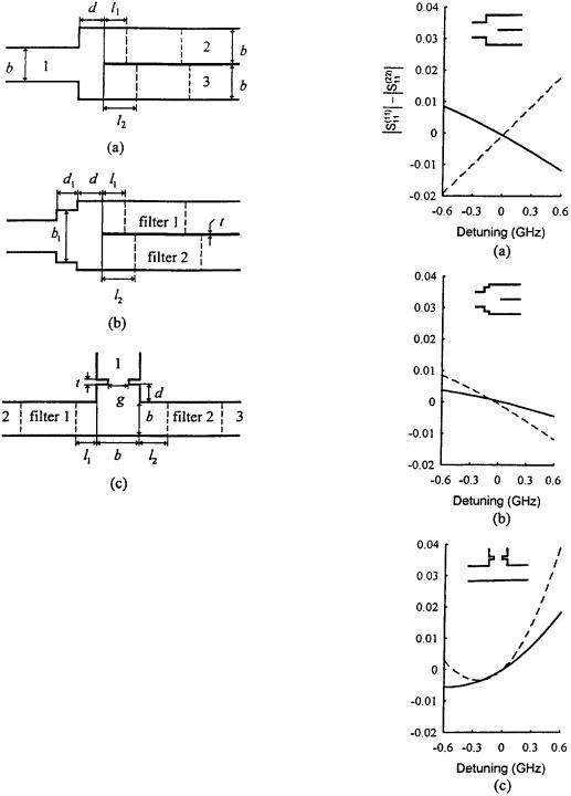
Figure 4. Various common ports.
ure 4c, where the variation is observed to be within 10y4 over the same band of operation. Obviously the configuration in Figure 4a is useful in the lower part of the waveguide band only.
Since the output ports of the common junction shown in Figure 4 are required to be mached at f01 and f02 , which are adjacent to fc j, it is required to know the dependence of <S1111. < y <S1122. < over the entire frequency band. Figure 5 shows the computed data dependence <S1111. < y <S1122. < for three types of common junctions discussed in this paper. The channel center frequencies are f01 s 27.1 GHz, f02 s 27.9 GHz, and fc j s 27.5 GHz for the one-step junction in Figure 4a. f01 s 38.2 GHz, f02 s 39 GHz, and fc j s 38.6 GHz for the two-step and E-T junctions in Figures 4b and c, respectively. The passband of all filters and the guard band between two channels is 0.4 GHz. Comparison of Figures 5a, b, and c show that the one-step junction is worse than the two-step one even in the lower part of the dominant mode waveguide band. It is interesting to note that the characteristics of the E-T junction are consider-
CAD of Wa¨eguide E-Plane Diplexers 109
Figure 5. Frequency response of various common ports.
ably different from those of the other two configurations. Although the E-T junction is more dispersive throughout the entire band, it is possible to effectively use the junction by satisfying eqs. 4. and 5. instead of 6..