


4.1 Basic Definitions of EMC |
71 |
Fig. 4.7 Paths of the receiver of the aircraft that receives EMI
occur, and it may affect the normal task of the system or limit the certain functions.
(4)The electromagnetic environment adaptability and spectrum supportability should be evaluated to minimize the limitations and vulnerability of systems, subsystems, and equipment. The evaluation should be performed through the life cycle which includes the stages of design, development, operation, etc.
4.2 Essences of Quantitative EMC Design
In order help our readers better understand the quantitative system-level EMC design, we will introduce and discuss the elements of electromagnetic coupling, the development phases of EMC, and system-level EMC in this section.
4.2.1 Identification of Electromagnetic Coupling Elements
Interference sources, coupling paths, and susceptive equipment are the three aspects (or elements) of EMC.
In practice, it is most difficult to identify the coupling path, because both the conductor and the air can be used as the transmission channel for the electromagnetic energy. Moreover, the electromagnetic fields involved in EMC problems often include the coexistence of near/far/inductive fields.
The following four examples illustrate the difficulty of coupling path identification.
Example 4.1 As shown in Fig. 4.7, the electromagnetic emission received by the receiver on the aircraft may come from three paths: circuit–circuit coupling of the receiver, field–circuit coupling between the receiving antenna and receiver cable, and the field coupling of receiving antenna.
The interference received by the circuit inside the receiver under conduction mode is referred to as the interference received through the circuit–circuit path. The emission received from field by the cable of the receiver is referred to as the interference
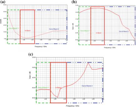
72 |
4 Basic Concepts of Quantitative System-Level EMC Design |
Fig. 4.8 Standing wave, main beam, and side lobe with changing frequency of an airborne receiving antenna. a Standing wave frequency characteristic; b main lobe frequency characteristic; c side lobe frequency characteristic
received through field–circuit coupling path. The emission received by the antenna, which is generated by other transmitting antennas or other EME signals, is referred to as interference received through the field–field coupling channel. Specifically, field coupling channel interference can be received by the main beam of the receiving antenna as shown in Fig. 4.8b, which is called direct coupling. The interference can also be received by the side lobe of the receiving antenna, as shown at the out-of-band part in Fig. 4.8c, which is called indirect coupling.
Example 4.2 Figure 4.9 shows the four coupling paths of the emission from the source to the receiver:
Path 1—The emission radiates directly from the source to the receiver.
Path 2—The emission radiates directly from the source and is then picked up by a power cable or signal/control cable connected to the receiver. The emission is thus conducted to the receiver.
Path 3—The emission radiates from the power, signal, or control cables of the source. Path 4—The emission is conducted directly from the source through the utility power cable or through a common signal cable/control cable to the receiver.

4.2 Essences of Quantitative EMC Design |
73 |
|||||||||||
|
|
|
|
|
|
|
|
|
|
|
|
|
|
|
|
|
|
|
|
|
|
|
|
|
|
|
|
|
|
|
|
|
|
|
|
|
|
|
|
|
|
|
|
|
|
|
|
|
|
|
|
|
|
|
|
|
|
|
|
|
|
|
|
|
Fig. 4.9 Schematic diagram of the four coupling paths of EMI from source to receiver
Based on the four coupling paths described above, it is obvious that the main mechanism of emission coupling from the source to the receiver is conduction and radiation.
Cables often appear in bundles in real-world projects. Thus, the emission carried by various power/signal/control cables connected to the source can be easily coupled to the power/signal/control cables connected to the receiver.
It is worth noticing that the emission caused by the cable is diffusive (whether it is sending out interference or picking up interference), so it is very difficult to solve the interference problem caused by the cable. Especially when the interference picked up by the cable is at the same frequency with the functional signal transmitted in the cable, the interference can hardly be filtered out. Therefore, it is fundamentally important to strictly control the coupling path caused by cables.
Example 4.3 Possible “antenna” coupling effects on radio frequency circuit boards (referred to as circuit boards in this section). An engineer tested a circuit board during the debug phase and found it was working properly. Then, the engineer made via holes at the four corners of the board to fix it into a case. However, after installation, the performance of the circuit board was abnormal. The board was then removed from the case, and the engineer found that the performance of the circuit board was inconsistent with the result of the previous test. The performance before punching could not be reproduced after several tests.
After careful investigation by an EMC specialist, it was found that the reason for this phenomenon was the mounting holes that the engineer made at four corners of the circuit board. The holes were located on the surface of the circuit board where electromagnetic currents were distributed. The holes actually cut the electromagnetic current and formed an “antenna” effect, which caused the system to operate abnormally. Since the cutting was irreversible, the performance of the circuit board could not be restored to the state before.
74 |
4 Basic Concepts of Quantitative System-Level EMC Design |
If the engineer could have analyzed the electromagnetic current on the board surface using the analysis software or the electromagnetic field scanning instrument before mounting the holes, we believe the above problem can be avoided.
Example 4.4 A metal partition was installed between two sections of a system. Later, the metal partition was removed in order to reduce the weight during a refit process. Then, it was found that an EMI problem occurred in the equipment located in the compartment.
The reason for this problem is that the metal partition has an electric shielding effect. The isolation between the front and rear cabin sections was reduced; thus, EMI problem occurred.
The four examples illustrate that there are many kinds of electromagnetic coupling paths. Only by understanding the coupling mechanism can we effectively avoid the emergence of new EMC problems.
4.2.2 Three Stages of EMC Technology Development
EMC studies have been through three stages of development: problem solving, standard design, and system design. The corresponding EMC research methods are problem-solving method, standard design method, and system design method.
(1)Problem-solving stage: In the design process of electrical and electronic systems, EMC is not fully considered. When there is an EMI problem later, engineers start to analyze the cause and find solutions.
Problem-solving method: The core concept of this method is “solving the problem only after it occurs.” This method is limited by many factors, and it is often difficult to implement the solution. Moreover, in terms of complex systems, it is even more difficult to solve the EMC problem.
(2)Standard design stage: Standardize EMC work and implement EMC design according to the standard requirements. At present, there is relatively complete EMC design specifications in the field of circuit boards and components design. Some effective qualitative or quantitative specification requirements have also been formed in grounding, bonding, shielding, cable layout, and static electricity prevention. EMC issues can be effectively reduced by designing in strict accordance with the specifications.
The commercial circuit design software that uses the design specifications plays an important role in reducing the interference of the electrical and electronic systems. As an example, the software may specify the minimum spacing limit for two parallel laid RF printed lines in order to avoid signal cross talk caused by too small spacing.
However, for complex systems, the significance of the standard specification is often “in theory” due to the variations and complexity of the system.
(3)System design stage: EMC performance of systems, subsystems, equipment, circuit boards, and components is analyzed and predicted, indicators are reason-