

MAX6734AKA
.pdfSingle-/Dual-/Triple-Voltage µP Supervisory Circuits with Independent Watchdog Output
VCC1, |
VCC |
VTH |
|
|
|
MAX6735AMAX6730A– |
VCC2 |
|
|
|
|||
RSTIN |
(MIN) |
|
|
|
|
|
RST |
|
tRP |
|
|
tRP |
|
|
|
|
|
|
||
WDO |
|
|
|
|
|
|
WDI |
|
<tWD-L |
<tWD-S |
>tWD-S |
<tWD-L |
|
MR |
|
|
|
|
|
|
|
|
|
|
|
tMR |
|
Figure 4. Watchdog Input/Output Timing Diagram (MR and WDO Connected)
Applications Information
Interfacing to µPs with Bidirectional Reset Pins
Microprocessors with bidirectional reset pins can interface directly with the open-drain RST output options. However, conditions might occur in which the push-pull output versions experience logic contention with the bidirectional reset pin of the µP. Connect a 10kΩ resistor between RST and the µP’s reset I/O port to prevent logic contention (Figure 5).
Falling VCC Transients
The MAX6730A–MAX6735A µP supervisors are relatively immune to short-duration falling VCC_ transients (glitches). Small glitches on VCC_ are ignored by the MAX6730A–MAX6735A, preventing undesirable reset pulses to the µP. The Typical Operating Characteristics show Maximum VCC_ Transient Duration vs. Reset
VCC2 VCC1 |
|
|
|
|
|
|
RESET TO |
|
|
VCC1 |
|
OTHER |
|
|
|
|
SYSTEM |
|
|
|
|
COMPONENTS |
|
|
MAX6731A |
|
10kΩ |
µP |
|
MAX6733A |
RST |
|||
|
RESET |
|||
MAX6735A |
|
|
|
|
VCC2 |
|
|
|
|
GND |
|
|
GND |
Figure 5. Interfacing to µPs with Bidirectional Reset I/O
______________________________________________________________________________________ 11
MAX6730A–MAX6735A
Single-/Dual-/Triple-Voltage µP Supervisory Circuits with Independent Watchdog Output
Threshold Overdrive graph, for which reset pulses are not generated. The graph was produced using falling VCC_ pulses, starting above VTH and ending below the reset threshold by the magnitude indicated (reset threshold overdrive). The graph shows the maximum pulse width that a falling VCC transient typically might have without causing a reset pulse to be issued. As the amplitude of the transient increases (i.e., goes further below the reset threshold), the maximum allowable pulse width decreases. A 0.1µF bypass capacitor mounted close to VCC_ provides additional transient immunity.
Watchdog Software Considerations
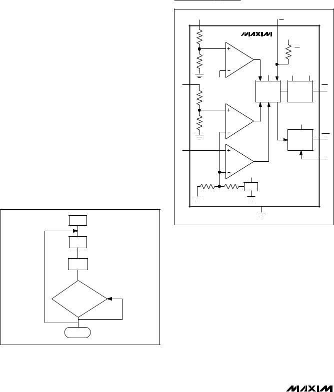
Setting and resetting the watchdog input at different points in the program rather than “pulsing” the watchdog input high-low-high or low-high-low helps the watchdog timer closely monitor software execution. This technique avoids a “stuck” loop, in which the watchdog timer continues to be reset within the loop, preventing the watchdog from timing out. Figure 6 shows an example flow diagram in which the I/O driving the watchdog input is set high at the beginning of the program, set low at the beginning of every subroutine or loop, and then set high again when the program returns to the beginning. If the program “hangs” in any subroutine, the I/O continually asserts low (or high), and the watchdog timer expires, issuing a reset or interrupt.
|
Functional Diagram |
|||
|
VCC1 |
MR |
|
|
|
MAX6730A– |
VCC1 |
|
|
|
|
|
|
|
|
MAX6735A |
MR |
|
|
|
|
PULLUP |
|
|
|
VCC1 |
VCC1 |
VCC2 |
|
VCC2 |
VREF |
|
|
|
|
RESET |
RESET |
RST |
|
|
TIMEOUT |
OUTPUT |
||
|
|
|||
|
PERIOD |
DRIVER |
|
|
|
|
|
VCC1 |
|
|
|
WATCHDOG |
WDO |
|
|
|
|
||
RSTIN |
|
TIMER |
|
|
|
|
|
|
|
|
|
|
|
WDI |
|
VCC1 |
|
|
|
|
REF |
|
|
|
|
VREF / 2 |
|
|
|
|
GND |
|
|
|
START
SET WDI
HIGH
PROGRAM
CODE
SUBROUTINE OR |
|
|
PROGRAM LOOP |
|
|
SET WDI LOW |
HANG IN |
|
SUBROUTINE |
||
SUBROUTINE |
||
COMPLETED |
|
RETURN
Figure 6. Watchdog Flow Diagram
12 ______________________________________________________________________________________

Single-/Dual-/Triple-Voltage µP Supervisory Circuits with Independent Watchdog Output
Standard Versions
|
|
|
|
PART |
|
TOP MARK |
|
MAX6730AUTLD3-T |
|
+ACIX |
|
MAX6730AUTSD3-T |
|
+ACJA |
|
MAX6730AUTRD3-T |
|
+ACIY |
|
|
|
|
|
MAX6730AUTZD3-T |
|
+ACJF |
|
|
|
|
|
MAX6730AUTVD3-T |
|
+ACJC |
|
|
|
|
|
MAX6731AUTLD3-T |
|
+ACJG |
|
|
|
|
|
MAX6731AUTTD3-T |
|
+ACJJ |
|
|
|
|
|
MAX6731AUTSD3-T |
|
+ACJI |
|
MAX6731AUTRD3-T |
|
+ACJH |
|
|
|
|
|
MAX6731AUTZD3-T |
|
+ACJL |
|
|
|
|
|
MAX6731AUTVD3-T |
|
+ACJK |
|
|
|
|
|
MAX6732AUTLTD3-T |
|
+ACHU |
|
|
|
|
|
MAX6732AUTSYD3-T |
|
+ACHZ |
|
MAX6732AUTSVD3-T |
|
+ACHY |
|
|
|
|
|
MAX6732AUTRVD3-T |
|
+ACHV |
|
MAX6732AUTSHD3-T |
|
+ACHX |
|
|
|
|
|
MAX6732AUTTGD3-T |
|
+ACIA |
|
|
|
|
|
MAX6732AUTSDD3-T |
|
+ACHW |
|
|
|
|
|
MAX6732AUTZWD3-T |
|
+ACIH |
|
|
|
|
|
MAX6732AUTYHD3-T |
|
+ACIF |
|
|
|
|
|
MAX6732AUTZGD3-T |
|
+ACIG |
|
MAX6732AUTYDD3-T |
|
+ACIE |
|
|
|
|
|
MAX6732AUTVHD3-T |
|
+ACIC |
|
|
|
|
|
MAX6732AUTWGD3-T |
|
+ACID |
|
|
|
|
|
MAX6732AUTVDD3-T |
|
+ACIB |
|
|
|
|
|
MAX6733AUTLTD3-T |
|
+ACII |
|
MAX6733AUTSYD3-T |
|
+ACIN |
|
|
|
|
|
MAX6733AUTSVD3-T |
|
+ACIM |
|
|
|
|
|
MAX6733AUTRVD3-T |
|
+ACIJ |
|
|
|
|
|
MAX6733AUTSHD3-T |
|
+ACIL |
|
|
|
|
|
MAX6733AUTTGD3-T |
|
+ACIO |
|
|
|
|
|
MAX6733AUTSDD3-T |
|
+ACIK |
|
MAX6733AUTZWD3-T |
|
+ACIW |
|
MAX6733AUTYHD3-T |
|
+ACIU |
|
|
|
|
|
PART |
TOP MARK |
|
|
MAX6733AUTZGD3-T |
+ACIV |
|
|
MAX6733AUTYDD3-T |
+ACIT |
MAX6733AUTVHD3-T |
+ACIR |
|
|
MAX6733AUTWGD3-T |
+ACIS |
|
|
MAX6733AUTVDD3-T |
+ACIQ |
|
|
MAX6734AKALTD3-T |
+AENS |
|
|
MAX6734AKASYD3-T |
+AENZ |
MAX6734AKASVD3-T |
+AENY |
|
|
MAX6734AKARVD3-T |
+AENU |
MAX6734AKASHD3-T |
+AENX |
|
|
MAX6734AKATGD3-T |
+AEOA |
|
|
MAX6734AKASDD3-T |
+AENV |
|
|
MAX6734AKAZWD3-T |
+AEOI |
|
|
MAX6734AKAYHD3-T |
+AEOG |
|
|
MAX6734AKAZGD3-T |
+AEOH |
MAX6734AKAYDD3-T |
+AEOF |
|
|
MAX6734AKAVHD3-T |
+AEOD |
|
|
MAX6734AKAWGD3-T |
+AEOE |
|
|
MAX6734AKAVDD3-T |
+AEOC |
|
|
MAX6735AKALTD3-T |
+AEOJ |
MAX6735AKASYD3-T |
+AEOO |
|
|
MAX6735AKASVD3-T |
+AEON |
|
|
MAX6735AKARVD3-T |
+AEOK |
|
|
MAX6735AKASHD3-T |
+AEOM |
|
|
MAX6735AKATGD3-T |
+AEOP |
|
|
MAX6735AKASDD3-T |
+AEOL |
MAX6735AKAZWD3-T |
+AEOX |
|
|
MAX6735AKAZID3-T |
+AEOW |
MAX6735AKAYHD3-T |
+AEOU |
|
|
MAX6735AKAZGD3-T |
+AEOV |
|
|
MAX6735AKAYDD3-T |
+AEOT |
|
|
MAX6735AKAVHD3-T |
+AEOR |
|
|
MAX6735AKAWGD3-T |
+AEOS |
MAX6735AKAVDD3-T |
+AEOQ |
|
|
Note: Sample stock is generally held on standard versions only. Standard versions have an order increment requirement of 2500 pieces. Nonstandard versions have an order increment requirement of 10,000 pieces. Contact factory for availability of nonstandard versions.
MAX6735A–MAX6730A
______________________________________________________________________________________ 13
MAX6730A–MAX6735A
Single-/Dual-/Triple-Voltage µP Supervisory Circuits with Independent Watchdog Output
Pin Configurations
TOP VIEW
RST |
1 |
|
6 |
VCC1 |
GND |
2 |
MAX6730A |
5 |
WDI |
MAX6731A |
||||
WDO |
3 |
|
4 |
MR |
|
|
SOT23-6 |
|
|
RST |
1 |
|
6 |
VCC1 |
GND |
2 |
MAX6732A |
5 |
WDI |
MAX6733A |
||||
WDO |
3 |
|
4 |
VCC2 |
|
|
SOT23-6 |
|
|
RST |
1 |
|
8 |
VCC1 |
GND |
2 |
MAX6734A |
7 |
RSTIN |
|
|
|
|
|
WDI |
3 |
MAX6735A |
6 |
VCC2 |
WDO |
4 |
|
5 |
MR |
SOT23-8
Typical Operating Circuit
+0.9V |
|
|
|
|
+1.8V |
|
|
|
|
|
|
VCORE |
|
|
|
+3.3V |
|
|
VCC2 |
VCC1 |
VCC |
VDD |
|
|
|
|
|
(I/O) |
(MEMORY) |
|
RSTIN |
|
RST |
RESET |
|
|
MAX6734A |
WDI |
I/O |
P |
|
|
MAX6735A |
|
|
|
|
PUSHBUTTON |
|
|
WDO |
NMI |
|
MR |
|
|
|
|
|
SWITCH |
|
|
|
|
|
|
|
GND |
|
|
GND |
___________________Chip Information
TRANSISTOR COUNT: 1073
PROCESS: BiCMOS
Selector Guide
|
|
|
|
|
|
|
|
|
|
PART NUMBER |
VOLTAGE |
RST OUTPUT |
MANUAL RESET |
WATCHDOG |
WATCHDOG |
||
|
MONITORS |
|
INPUT |
OUTPUT |
||||
|
|
|
|
|
||||
|
|
|
|
|
|
|
|
|
|
MAX6730A |
1 |
Open Drain |
√ |
|
√ |
Open Drain |
|
|
MAX6731A |
1 |
Push-Pull |
√ |
|
√ |
Push-Pull |
|
|
|
|
|
|
|
|
|
|
|
MAX6732A |
2 |
Open Drain |
— |
|
√ |
Open Drain |
|
|
|
|
|
|
|
|
|
|
|
MAX6733A |
2 |
Push-Pull |
— |
|
√ |
Push-Pull |
|
|
|
|
|
|
|
|
|
|
|
MAX6734A |
3 |
Open Drain |
√ |
|
√ |
Open Drain |
|
|
|
|
|
|
|
|
|
|
|
MAX6735A |
3 |
Push-Pull |
√ |
|
√ |
Push-Pull |
|
|
|
|
|
|
|
|
|
|
14 ______________________________________________________________________________________

Single-/Dual-/Triple-Voltage µP Supervisory Circuits with Independent Watchdog Output
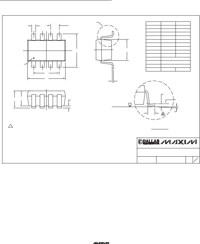
Package Information
(The package drawing(s) in this data sheet may not reflect the most current specifications. For the latest package outline information go to www.maxim-ic.com/packages.)
|
|
|
6LSOT.EPS |
PACKAGE OUTLINE, SOT 6L BODY |
|
|
|
21-0058 |
G |
1 |
1 |
MAX6735A–MAX6730A
______________________________________________________________________________________ 15
MAX6730A–MAX6735A
Single-/Dual-/Triple-Voltage µP Supervisory Circuits with Independent Watchdog Output
Package Information (continued)
(The package drawing(s) in this data sheet may not reflect the most current specifications. For the latest package outline information go to www.maxim-ic.com/packages.)
|
|
SEE DETAIL "A" |
|
|
|
|
|
.EPS |
|
|
|
|
SYMBOL |
MIN |
MAX |
|
8L |
||
|
b |
e |
|
|
|
||||
|
|
|
A |
0.90 |
1.45 |
|
SOT23, |
||
|
CL |
|
|
|
|
||||
|
|
|
|
A1 |
0.00 |
0.15 |
|
|
|
|
|
|
|
|
|
|
|||
|
|
|
|
|
A2 |
0.90 |
1.30 |
|
|
|
|
|
|
|
b |
0.22 |
0.38 |
|
|
|
|
|
|
|
C |
0.08 |
0.22 |
|
|
|
|
|
|
|
D |
2.80 |
3.00 |
|
|
|
CL |
E |
CL |
E1 |
E |
2.60 |
3.00 |
|
|
|
E1 |
1.50 |
1.75 |
|
|
||||
|
|
|
|
|
|
|
|||
|
|
|
|
|
L |
0.30 |
0.60 |
|
|
|
PIN 1 |
|
|
|
L2 |
0.25 BSC. |
|
|
|
|
|
|
|
e |
0.65 BSC. |
|
|
||
I.D. DOT |
|
|
|
|
|
||||
|
|
|
e1 |
1.95 REF. |
|
|
|||
(SEE NOTE 6) |
|
|
|
|
|
||||
|
|
|
|
|
0 |
0° |
8° |
|
|
|
e1 |
|
|
|
|
|
|
|
|
|
D |
|
|
|
|
|
|
|
|
|
|
|
|
C |
|
|
|
|
|
|
CL |
|
|
|
|
|
|
|
|
|
|
|
|
|
|
L2 |
|
|
|
A |
A2 |
A1 |
|
|
|
|
GAUGE PLANE |
|
|
|
|
|
|
|
|
|
|||
|
|
|
|
|
|
|
|
|
|
|
|
|
|
SEATING PLANE C |
|
|
|
|
|
|
|
|
|
|
L |
0 |
|
|
|
NOTE: |
|
|
|
|
|
|
|
||
|
|
|
|
|
|
|
|
||
1. ALL DIMENSIONS ARE IN MILLIMETERS. |
|
|
|
|
|
|
|
|
|
2. FOOT LENGTH MEASURED FROM LEAD TIP TO UPPER RADIUS OF |
|
DETAIL "A" |
|
|
|
||||
HEEL OF THE LEAD PARALLEL TO SEATING PLANE C. |
|
|
|
|
|
||||
|
|
|
|
|
|
|
|||
3. PACKAGE OUTLINE EXCLUSIVE OF MOLD FLASH & METAL BURR. |
|
|
|
|
|
|
|||
4. PACKAGE OUTLINE INCLUSIVE OF SOLDER PLATING. |
|
|
|
|
|
|
|
||
5. COPLANARITY 4 MILS. MAX. |
|
|
|
|
|
|
|
|
|
6. PIN 1 I.D. DOT IS 0.3 MM Ø MIN. LOCATED ABOVE PIN 1. |
|
PROPRIETARYINFORMATION |
|
|
|
|
|||
7. SOLDER THICKNESS MEASURED AT FLAT SECTION OF LEAD |
|
|
|
|
|
||||
|
TITLE: |
|
|
|
|
|
|||
BETWEEN 0.08mm AND 0.15mm FROM LEAD TIP. |
|
PACKAGE OUTLINE, SOT-23, 8L BODY |
|
||||||
8. MEETS JEDEC MO178 VARIATION BA. |
|
|
APPROVAL |
DOCUMENT CONTROL NO. |
REV. |
1 |
|
||
|
|
|
|
|
|||||
|
|
|
|
|
|
21-0078 |
E |
|
|
|
|
|
|
|
|
|
1 |
||
Maxim cannot assume responsibility for use of any circuitry other than circuitry entirely embodied in a Maxim product. No circuit patent licenses are implied. Maxim reserves the right to change the circuitry and specifications without notice at any time.
16 ____________________Maxim Integrated Products, 120 San Gabriel Drive, Sunnyvale, CA 94086 408-737-7600
© 2006 Maxim Integrated Products |
is a registered trademark of Maxim Integrated Products, Inc. |
Heaney