Embedded system engineering magazine 2006.05,06
.pdfFPGA-centric computing architecture
<Written by> Dr. Malachy Devlin, Nallatech </W>
A personal view on a different route to high
IHAVE SPENT most of my career working on architectures that deliver performance and from my experiences in constructing processing sys-
tems with different architectures and processing devices, I see the greatest potential for FPGA-centric computing.
The initial driver behind Nallatech’s formation, in 1993, was creating the best high-per- formance computing systems without a bias to a particular processing solution. In 1993, the typical technique used to gain additional processing capability was to put many microprocessors into the system to create a parallel processing system. One processor developed from the ground up for this approach was the Transputer processor developed by Inmos. We took our knowledge of parallel processing and used it to create heterogeneous microprocessor systems. These systems included processors such as the Transputer, Texas Instruments C80 and C40 and also Intel’s i860 devices. We had previously used FPGAs mainly for glue logic applications, but came to appreciate that FPGAs were great devices for handling I/O and in particular fast I/O. Because they could be directly coupled to the I/O devices themselves, they optimised the process of transferring the data and minimized the latency in getting data in and out of the system. So we built architectures with parallel microprocessor systems using FPGAs to assist in offloading data I/O and for simple mathematical operations. These systems used the 4K series from Xilinx, an infant in terms of today’s FPGAs capabilities.
A processor change
An interesting thing happened in 1998. Many of the processors that we used were reaching their end of life and were not recommended for new designs. Furthermore, Xilinx was creating their Virtex family. This created a step change in the capabilities of FPGAs and came with a roadmap that promised to continue to drive the capacity of future families of FPGAs. FPGAs were now able to take a more central role within high-performance computing systems and had reached the critical point where they could handle the system management, data management and data processing. This
offered greater flexibility in how systems were architected allowing the development of the DIME modular system for FPGA-centric systems. Utilizing the FPGA as the central processing engine enabled us to have very high I/O bandwidths, well beyond what was available with microprocessors, and with the reconfigurable nature of the FPGAs we could choose the type and protocol of the I/O, based on the application implemented.
This architectural approach created two issues. The first was that microprocessors were still better at certain tasks, such as floating point performance and complex serial control algorithms. This was easily accommodated by using the microprocessor as a coprocessor to the FPGA to provide these specialised operations.
Tools
The other issue we needed to address was that of tools. We were already familiar with microprocessor tools that enabled the detection, reprogramming and data transfer to the system under development from a GUI. This feature was also created in 1998 when we created DIME to provide plug and play capability to the FPGA system. We created an intelligent software interface called FUSE which enabled the control and management of multi-FPGA systems. This software would enable any FPGA within the system to be reconfigured and enabled data transfers over an abstracted interface.
With the first generation of DIME we learned a lot regarding FPGA-centric systems, their usage models and the requirements from our customers for the next generation of product. FPGAs and the associated technology moved on, so we evolved our architecture to DIME-II. DIME-II extended the I/O bandwidth capability and was engineered to ensure that we could support several more generations of FPGAs. Today we are shipping DIME-II with Xilinx Virtex-4 for our highest levels of performance.
Communication framework
The key driver to wider adoption of the technology is continuing to make FPGA-centric
Figure 1: Increasing FPGA-centric computing
systems easier to use. To manage multiFPGA systems we created DIMEtalk, a design tool and management system for the rapid design of a communications framework for FPGAs through a GUI. It provide the connection of memories, IP cores, embedded processors cores and external multi-gigabit transceivers and greatly simplifies the process of creating the system framework: application engineers can focus on their algorithms rather than the low level details of pin outs or memory control.
DIMEtalk also provides linking for highlevel language tools: today, it is possible to design FPGAs from C or Simulink without needing to understand VHDL or Verilog. FPGAs are truly becoming a processing technology that can be fully utilized by software engineers.
Moving forward, there continues to be a lot of emphasis on making FPGAs more accessible and easier to use by simplifying the programming model for them. The goal is to provide the highest performance in the simplest product. The other key development going on is that many vendors and users are collaborating to create standards associated with FPGAs. This includes the work being done by the FPGA High Performance Computing Alliance (FHPCA), OpenFPGA (www.openfpga.org) and VITA. This will lead to focus and stability in the marketplace and enable developments which will allow systems to be created based on open standards that ensure interoperability. A critical component to enable the market to flourish is the continued developments in FPGA-centric computing architectures. <End/>
www.xxx.com
</Feature>
ESE Magazine May/June 06
31
<In-Depth>
ESE Magazine May/June 06
32
In-Depth: Security and encryption are vital ingredients
<Written by> Martin Whitbread </W>
Where should you be applying security in your next project?
THERE ARE MANY different consider in security. This overview at the different approaches
offer in different areas of the
In the OS
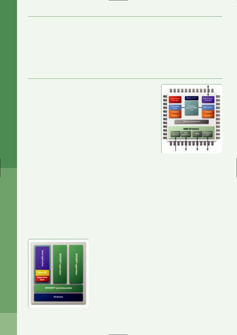
The increasing use of internet trading worked systems of all descriptions construction of highly secure systems a of many developments. The use of a OS as part of the system can leave open for intruders and some very system crashes. Greenhills has approach to solving this problem by
protected environment, known as Padded which allows users to run commercial type operating systems such as Linux, as guest operating systems in user mode. Multiple padded cell applications can run concurrently in a single physical computer, each hosting its own guest OS. An impenetrable wall around each guest operating system ensures that errant, insecure or malicious code can never compromise security. Integrity PC combines the Integrity OS with Green Hills Software’s Padded Cell. It protects secure applications in several ways:
●Each partition has its own memory-protected virtual address to ensure that software cannot corrupt, disrupt, or spy on another partition.
●Guest OSs and their applications run as user mode Integrity applications. They cannot
defence, Wind River has produced a Secure |
Figure 2: ARM1176JZF-S |
RTOS (SRTOS) that exploits experience with its |
|
|
|
ARINC653 RTOS. The new system applies |
|
MILS (Multiple Independent Levels of Security) |
|
concepts in order to meet Evaluation |
|
Assurance Level 7 (EAL 7) of the Common |
|
Criteria of Information Technology Security |
|
Evaluation. The VxWorks SRTOS consists of a |
|
secure kernel that is based the Separation |
|
Kernel Profile, a security policy database, ref- |
|
erence monitor, secure audit log and all other |
|
common MILS components. It controls co-resi- |
|
dent high and low level security applications, |
|
using a time and space scheduler that has |
|
been reviewed by safety auditors. MILS sys- |
|
tem designers can place device drivers in the |
|
kernel space, middleware partitions or appli- |
|
cation partitions. |
|
|
In the CPU |
|
|
|
Providing security at the CPU hardware level is |
|
|
|
now becoming increasingly relevant for com- |
|
|
|
panies providing the processor hardware, or |
|
|
|
the design technology to manufacture it. |
|
|
|
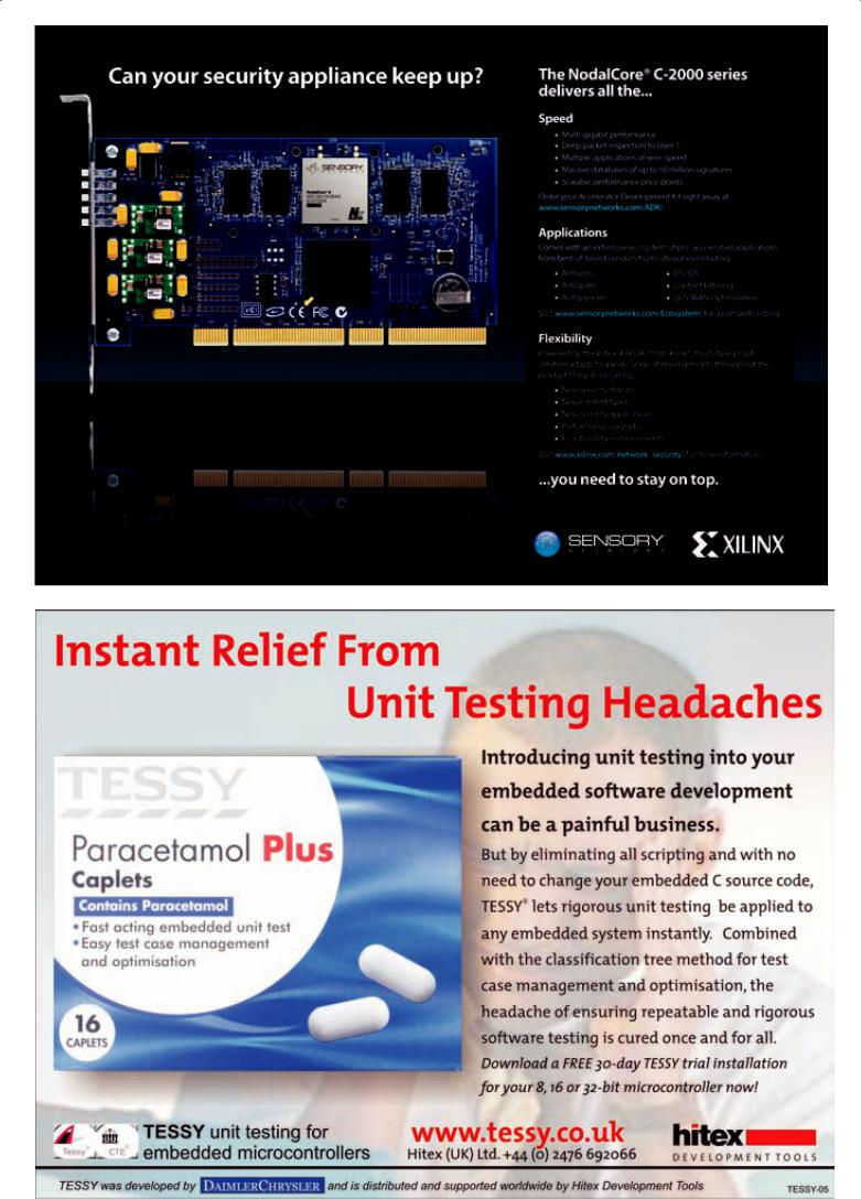
ARM’s TrustZone technology is aimed at secur- |
|
|
|
ing customer products such as mobile phones, |
|
|
|
PDAs or other systems running operating sys- |
|
|
|
tems such as Symbian OS, Linux and Windows |
|
|
|
CE. This technology is implemented within the |
|
|
|
core itself. A new mode, ‘Secure Monitor’, |
|
|
|
within the core acts as gatekeeper and reliably |
|
|
|
switches the system between secure and non- |
|
|
Figure 1: Padded cells in Integrity PC |
secure states. When this monitor switches the |
|
|
system to the secure state the processor gains |
tion server such as Remote Authentification |
||
|

Dial-In User Service (Radius) to use in the Nucleus 802.11i software. This also supports Temporal Key Integrity Protocol (TKIP) and Counter Mode with Cipher Block Chaining Message Authentification Code Protocol (CCMP) with Advanced Encryption Standard (AES) for WPA and IEEE802.11i encryption. Nucleus software also has the option to enable users to configure IEEE802.11i specific pair-wise master-key (PMK) caching support for fast roaming.
Another technique that has proved very effective in remote control systems is code hopping. Early remote control systems were wide open to snooping. The use of short fixed code combinations made these systems extremely vulnerable. The use of larger codes and code hopping techniques of the type available in Microchip’s Keeloq makes scanning or attempts at code replication, pointless. In Keeloq a large number of possible combinations are provided by a 66-bit transmission code. A 32-bit encrypted portion provides for more than 4 billion combinations. In addition a 34-bit fixed portion eliminates any chance of guessing the code. The system never responds twice to the same transmitted code. A different code is transmitted each time, with no apparent relationship between any one code and the previous or next code. If a transmitter
is activated out of range more than 16 times synchronisation with the receiver is lost. This is restored by two successive activations in range.
In the code
Encryption is an evolving technology that keeps coming up with ‘uncrackable’ codes which are subsequently broken with relative ease. This has been the case for thousands of years. Earlier data encryption codes such as the DES 56-bit key are now easily broken. A typical 1024-bit RSA asymmetric key is said to be about as secure as an 80-bit symmetric key. AES key sizes range from 128-bits to 256-bits. To provide security equivalent to AES, RSA public key sizes would have to range from 3,072 to 15,000 bits long. A solution that looks like resolving this problem is Elliptic Curve Cryptography (ECC) which uses smaller key sizes. This is the basis for Certicom’s Security Architecture. While a 128-bit symmetric would require an RSA or DH key of 3,072 bits in order to provide equal protection, an ECC key of 256 bits would provide just as much security. The benefits increase greatly for larger sizes, a 256-bit symmetric key would need an RSA of 15,000 bits but only a 512-bit ECC key. The savings in power drain, memory and CPU loading are considerable. For hardware implemen-
Contacts
ARM
www.arm.com
Certicom
www.certicom.com
Green Hills Software
www.ghs.com
Mentor Graphics
www.mentor.com/embedded/
Microchip
www.microchip.com
Wind River
www.windriver.com
tation, the savings of ECC-163 over RSA-1024 are factor of 10 in the number of gates used.
Communication overheads are also much lower, a significant factor in embedded systems. Using key agreement methods such as ECMQV for ECC-163 only a single data packet needs to be exchanged, a total of 326 bits or 41 bytes of payload. This allows a much more efficient use of communications bandwidth. Effective encryption in embedded systems becomes a possibility and system performance is unlikely to be greatly affected by its application. <End/>
before you start development...
... for the best in embedded tools and software...talk to SDC!
w w w. s d c s y s t e m s . c o m SDC
Systems

</Feature>
ESE Magazine May/June 06
34
The building blocks of security
<Written by> Uriah Pollock, Mentor Graphics </W>
Different approaches to message encryptionallow trade-offs between level of security and processing time.
THERE ARE MANY methods devices around the world
data and privacy. It credit card or a digital
management protected IP that secured. This information may be locally on the device or transmitted network using a protocol such as the Sockets Layer (SSL), Internet Security (IPsec) or IEEE 802.11i, also as Wi-Fi Protected Access 2. These along with other security-related
and techniques, have a set of algorithms in common, which can be thought of as the building blocks of security. This article will focus primarily on defining the building blocks while touching briefly on the methods in which they are used.
Symmetric key encryption
The main algorithms that are used to encrypt data are known as symmetric key encryption algorithms. These algorithms have one key quality that makes them well suited for this task; they are faster than their asymmetric key encryption algorithm counterparts. Since large amounts of data are usually encrypted or decrypted at a time, this quality is very important. For example, you may want to secure a
how to |
communicate this agreed upon key |
Figure 3: Hashing algorithms. |
|
||
without |
someone else viewing it. Symmetric |
|
key algorithms are also reversible. This means that once a piece of data is encrypted, it can be decrypted. This is not the case for hashing algorithms (more on this below). The Data Encryption Standard (DES) and the Advanced Encryption Standard (AES) are examples of symmetric key algorithms.
Asymmetric key encryption
Asymmetric key encryption algorithms, on the other hand, are more computationally intensive and therefore much slower than symmetric key algorithms. These are predominately used by networking security protocols at the start of a secure session, not during normal network communication. Usually when secure
Figure 1: Symmetric key encryption.
Figure 2: Asymmetric key encryption.
symmetric encryption algorithms are used at that time.
The other important difference in how asymmetric key encryption algorithms function is that, unlike symmetric encryption algorithms, they use two keys. One key is used for encryption and a second, different key is used for decryption (see figure 2). This is what enables the exchange of encryption keys before a secure session starts, as mentioned earlier. Examples of these are Rivest Shamir
Adleman (RSA) and Diffie-Hellman (DH). These
www.mentor.com
types of encryption algorithms are also known

Accelerating cryptographic algorithms
<Written by> Steve Leibson, Tensilica, Inc. </W>
Configurable processors can speed up cryptographic algorithms.
CONVENTIONAL WISDOM says that microprocessor implementations of cryptoalgorithms are too slow for dataplane applications. However, this wis-
dom is wrong when the processor’s ISA (instruc- tion-set architecture) is tailored for optimal algorithm performance. The addition of a mere handful of instructions to a configurable processor core using an automated processor generator can accelerate application performance to hardware speeds. There are many encryption and decryption schemes in use and all are amenable to performance enhancement through ISA tailoring. This article discusses ways to accelerate two popular cryptographic schemes: DES and AES.
DES: oldie but goodie
While DES is often criticized for its relatively short 56-bit key, a simple algorithm variant called triple-DES (3DES) extends the key to 168 bits by iterating the DES algorithm three times with different keys. Even though DES has been around since 1977, there is still no known attack on 3DES that is much faster than exhaustive search. Consequently, the 3DES encryption algorithm is used for both the Secure Shell tools (SSH) and the Internet Protocol for Security (IPSEC). General-purpose microprocessors are too slow to encrypt or decrypt high-speed digital-media and Internet-packet streams. However, tailoring a configurable microprocessor’s ISA by adding only four instructions can improve DES algorithm performance by 40x to 80x.
Firmware DES implementations run slowly on general-purpose RISC processors due to the algorithm’s numerous bit permutations. However, these permutations are easy to implement in hardware and they execute quickly because each permutation corresponds to simple wire scrambling (no gates required). Likewise, the DES algorithm’s 28-bit rotations are inefficient on general-purpose, 32-bit RISC microprocessors, which lack 28-bit rotation instructions. However, these rotations are easy to perform in custom hardware.
Tailoring a microprocessor’s ISA to improve algorithm performance essentially adds DES - specific hardware to the processor, which gives the processor the execution speed of DES hardware while retaining the processor’s firmware
programmability. Only three new processor registers and four new instructions are needed to accelerate the DES code. The three new registers are: 28-bit C and D registers and a 64-bit DATA register. The custom DES instructions are:
●STKEY (move data to C and D)
●STDATA (move data to DATA)
●LDDATA (move DATA to general-purpose registers)
●DES (inner-loop iteration instruction). Adding custom DES registers and instructions reduces the code-and-data memory footprint from 5560 bytes to only 156 bytes. ISA tailoring adds 5,000 gates to the processor but saves 45,216 bits of RAM. Hence, the net silicon cost for the processor with the DES extensions is less than 5,000 gates yet the resulting DES algorithm runs much faster.
New crypto on the block: AES
In 1997, the US National Institute of Standards and Technology (NIST) chose the Rijndael block cipher for AES (the Advanced Encryption Standard) from amongst several candidates. The AES cipher encrypts plaintext to ciphertext on a block-by-block basis. The plaintext block is conceptually stored and operated upon in a 16-byte state array. The AES cipher performs transformations on rows or columns of the state array. AES encryption consists of four transformations:
●SubBytes: performs byte-wise substitutions for each byte in the state array using a fixed table
●ShiftRows: rearranges the bytes within the state array
●MixColumns: treats each column of the state array as a polynomial and performs a Galois field multiplication with a fixed 4x4 matrix
●AddRoundKey:performs byte-wise Galois field additions using bytes from the key schedule
Porting the AES cipher to a general-purpose RISC processor is simple but the performance of such an implementation is usually unacceptable. Consequently, SOC designers will generally rule out firmware-only implementations except when bandwidth requirements are low.
ISA tailoring, as described above in the DES example, can transform a configurable processor into a fast, efficient AES engine by adding
Figure 1: Simplified DES algorithm
www.tensilica.com
</Feature>
ESE Magazine May/June 06
35

</Feature>
ESE Magazine May/June 06
36
Keeping security fast and relevant
<Written by> Mick Johnson, Sensory Networks </W>
FPGA based security processors are the route to network security.
FFECTIVE SAFETY is getting much |
|
|
|
to deliver. The increase in network |
|
|
|
attacks, combined with increases in net- |
|
|
|
Ework traffic, have lead to a need for |
|
|
|
hardware acceleration in security appliances. |
|
|
|
Multiple classes of threat, such as worms, virus- |
|
|
|
es, spam and spyware, require multiple threat |
|
|
|
signature databases for effective protection. A |
|
|
|
new breed of co-processor known as a content |
|
|
|
processor bridges the key bottleneck of scanning |
|
|
|
network traffic streams and matching against |
|
|
|
multiple databases to provide effective protec- |
|
|
|
tion from blended threats. |
|
|
|
Accelerated content security |
|
|
|
Figure 1: A fast content processor improves processor speed. |
|
||
When building a security appliance, the two key |
|
||
issues are keeping the speed up and attackers |
|
|
|
|
|
|
|
out. For antivirus, antispam, IPS, antispyware |
|
|
|
and many other functions this relies on scanning |
|
|
|
traffic and matching against a signature data- |
|
|
|
base that’s kept regularly updated. As these |
|
|
|
databases get bigger, and traffic gets faster, |
|
|
|
memory has become the main bottleneck. |
|
|
|
Standard systems work best with sequential |
|
|
|
access or if the whole database fits into L1 and |
|
|
|
L2 cache – now close to an impossible scenario. |
|
|
|
To handle this many appliances offload pattern- |
|
|
|
matching and other key functions to a fast con- |
|
|
|
tent processor (see Figure 1) with its own mem- |
|
|
|
ory and processing power. With strict bounds on |
|
|
|
latency and rapid lookups even for massive |
|
|
|
databases, this keeps security appliances run- |
|
|
|
ning at gigabit speeds even with deep-content |
|
|
|
inspection turned on. |
|
|
|
Changeable solution |
|
|
|
We’ve all seen the security threat landscape |
|
|
|
change over the past few years. Spyware seem- |
|
|
|
ingly came out of nowhere to be on everyone’s |
|
|
|
lips today, while VoIP spam is just over the hori- |
|
|
|
zon. Every time we turn around there’s a new |
|
|
|
threat or document type that alters the process- |
|
|
|
ing requirements. The ASIC-based solutions that |
|
|
|
hardware engineers are accustomed to are grad- |
|
|
|
ually being shown up as too cumbersome. Fixed- |
|
|
|
logic designs just don’t suit a problem when the |
|
|
|
goalposts keep shifting. |
|
|
|
For example, say in the next couple of years |
|
|
|
a new type of virus becomes prevalent – embed- |
functions available after the initial sale as an |
|
|
www.sensorynetworks.com |
|
||
ded in a new document format. Scanning these |
add-on, an additional revenue stream. As well |
|
|
|
|
||

REPRINT
SERVICE
If you would like reprints of any article published in this magazine or pdf files for use on your Website contact Dave on +44 (0) 207 681 7914 or email: dave@edaltd.co.uk
To advertise call +44 (0) 207 681 1000 and ask for Steve Banks
</Feature>
ESE Magazine May/June 06
38
When is slow fast?
<Written by> Øyvind Strøm, Atmel Corporation </W>
Atmels’s AP7000 is aimed at reducing power in portable appliances.
ATHE NUMBER of features in cell phones, personal media players, video recorders and still cameras increases, the extra processing puts a drag on bat-
tery life. However, the capacity of batteries is not keeping up, leaving users with reduced playback time or active-time.For example, the processors, LCD, RF and earphones in a typical hand-held media player consume close to 4 Watts (table 1), while the batteries typically used in these applications are 3.7V with 900-2000 mAh energy.
Since processing alone accounts for 1/3 of total system power consumption with the DSP and MCU, the processor is the obvious target for improving system power consumption, and the obvious thing to do is increase processor throughput so applications can be run with slower clocks. SoC-level integration and bus clock management is also critical to be able to remove power-hungry components like the DSP.
Atmel’s AP7000 has taken this approach by integrating the company’s high-throughput AVR32 MCU/CPU core with a vectored multiplier coprocessor, on-chip SRAM, CPU caches, memory management unit, and multiple on-chip DMA controllers. Peripherals include bit-stream audio DAC, TFT/STN LCD & HDD controllers, 480 Mbps USB 2.0 with on chip transceivers (PHY), two 10/100 Ethernet MACs adds to the connectivity of the application, while serial interfaces like RS232, USART, I2S, TWI/I2C, SPI, PS/2 and several synchronous serial modules (SSC) supporting most serial communication protocols help replace the majority of external components in these systems. The bus structure allows clocks to be set to individual frequencies in four domains (CPU, bus matrix, peripheral bridge A and peripheral bridge B) to minimize power consumption at all times.
AVR32 CPU
Atmel’s AVR32 DSP/MCU core was built from
|
DSP+MCUMP |
AP7000PMP with AVR32 |
CPU |
0,41 |
0,25 |
LCD panel |
1,06 |
1,06 |
Bluetooth |
N/A |
N/A |
CDMA |
|
N/A |
|
N/A |
802.11b |
|
0,25 |
|
0,25 |
SDRAM |
|
0,56 |
|
0,56 |
LCD backlight |
|
0,2 |
|
0,2 |
Flash memory |
|
0,03 |
|
0,03 |
Off-chip buses |
|
0,62 |
|
0,62 |
DSP |
|
0,86 |
|
By CPU |
Total |
|
3,99 |
|
2,97 |
|
|
|
|
|
Table 1: Media Player power comparison. Typical power consumption figures (Watts). Source: Research paper by Shim, Cho, Chang at the university of Korea (ESTIMedia2004) and Atmel.
the ground up specifically to lower power consumption by increasing computational throughput and using a much slower clock.
The AVR32 core puts special emphasis on 1) maximizing the use of computational resources with a seven stage pipeline and three parallel sub-pipelines that supports automatic data forwarding and out-of-order execution; 2) using pointer arithmetic to minimize the cycle count for load store operations, 3) accurate branch prediction with zero-penalty branches and 4) maximizing code density to reduce cache misses.
Vector co-processor
A vector multiplier co-processor executes scaling and color-space conversion and other matrix multiplication operations independently of the AVR32 CPU, keeping throughput high.. When used for image scaling operations, the AP7000’s vector multiplication co-can processor increases image scaling performance by as much as ten times.
Direct memory access
The AP7000 provides several flexible Direct Memory Access (DMA) mechanisms that can handle two simultaneous data transfers between peripherals and memory, or between two memo-
ally lower power consumption. For example, the AVR32 core can execute quarter-VGA MPEG4 decoding at 100 MHz, while competing processors need clocks of 150 MHz to 266 MHz for the same function. By running a slower clock, the AP7000 can reduce system power consumption by 1/3.
Dynamic frequency scaling
In most high-end 32-bit MCUs, the fastest peripheral determine the clock rate for the entire multilayered bus structure. In contrast, the AP7000 provides two peripheral bus bridges that can have different clock rates for high-speed and low speed peripherals. The AP7000 processor uses dynamic frequency scaling algorithms to configure individually the clock frequency of the two bridges, the CPU’s internal clock and the bus matrix. For example, the CPU clock, bus matrix and high speed bridge frequencies can be turned down, while the low speed bridge is maintained at a low frequency for a Bluetooth or IrDA data transfer. Clock frequencies changes take one CPU cycle, by writing a 32-bit value to a configuration register. Internal low-power oscillators and PLLs are running and locked and do not require any time for calibration between the frequency changes, thus making all changes really instant.
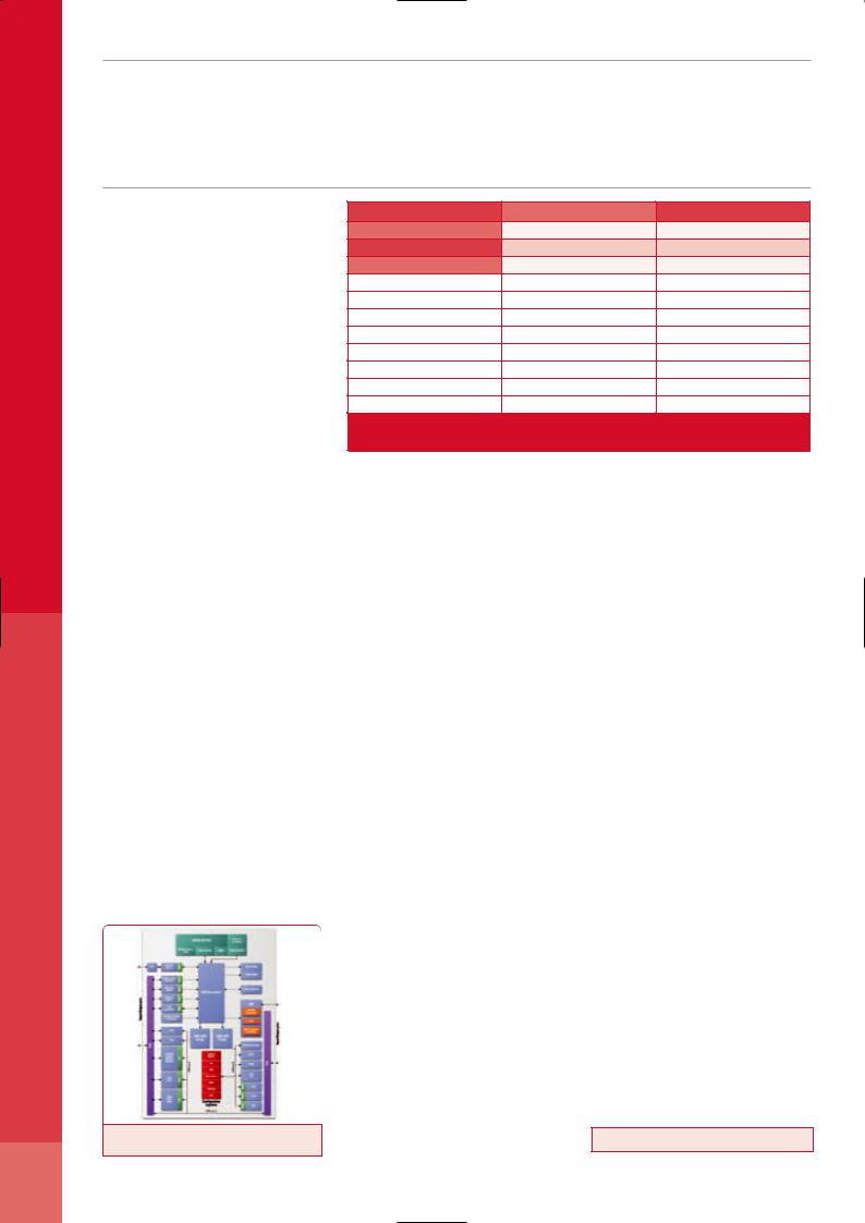
Figure 1: AP7000 block diagram |
the job done at a slower clock rate and proportion- |
www.atmel.com |
|
|