

EIA-364-109 standard.Loop inductance measurement test procedure for electrical connectors
.pdfEIA-364-109
Page 6
3 Test specimen
3.1 Description
For this test procedure the test specimen shall be as follows:
3.1.1 Connectors
A connector or mated connector pair.
3.1.2 Sockets
A socket and test device.
4 Test procedure
4.1Set the vector network analyzer to measure S11 for loop inductance.
4.2Calibrate the equipment and fixture according to the manufacturer’s specifications using the calibration standard. The calibration plane is to be directly at the probe interface to the fixture; see 2.2.4.1 for more detailed information. Unless otherwise specified in the referencing document it is recommended that the following equipment settings be used:
Smith chart format,
set network analyzer to display inductance values,
minimum of 401 measurement points,
frequency span – conduct both wideband and narrowband sweeps,
no smoothing,
averaging set to 16 or higher.
NOTE “Wideband” sweep is typically the full range of the network analyzer and “narrowband” sweep is over a limited range (for example 100 MHz wide).
EIA-364-109
Page 7
4.3 Fixture measurement
Position the probes to touch the interface pads of the test board characterization structure. Measure and record the loop inductance of the fixture from the Smith chart at the frequency(s) of interest.
NOTE A loop inductance vs. frequency graph may be generated through the use of data acquisition software and spreadsheet software, if specified in the referencing document.
EIA-364-109
Page 8
4.4 Specimen measurement
4.4.1Connect the probe to the fixture interface pad of the driven line with the specimen installed as shown in figure A.1. Terminate the far end of the driven line in an electrical short circuit to the return conductor(s).
4.4.2Place the specimen a minimum of 5 cm from any object that may introduce error into the measurement.
4.4.3Measure and record the loop inductance over the specified test frequency range or discrete frequencies.
4.4.4Calculate the specimen loop inductance by subtracting the fixture loop inductance, (see 4.3) from the specimen plus fixture loop inductance, see 4.4.3.
NOTE — If specified in the referencing document, a loop inductance vs. frequency graph may be generated through the use of data acquisition software and spreadsheet software.
4.4.5If requested, repeat 4.4.1 through 4.4.4 on multiple conductors throughout the specimen.
4.4.6When additional measurements with different test frequencies or ranges are required perform the calibration step defined in 4.2, then repeat 4.4.1 through 4.4.5 as necessary.
5 Details to be specified
The following details shall be specified in the referencing document:
5.1Measurement frequency range and/or discrete frequency(s)
5.2Special requirements with respect to the fixture, and the short circuit, (see 2.2.1.4) construction and electrical properties of each.
5.3Signal/ground pattern, including the number and location of signal and grounds. It is recommended that enough locations within the specimen be measured to take into account the varying loop inductances within the specimen
5.4Location of the drive signal connection point, location of the return signal connection point and connections to be made to adjacent pins, if any
5.5Specimen environment impedance if other than 50 ohms
5.6Plots, if desired, and Smith charts or loop inductance vs. frequency graphs
EIA-364-109
Page 9
6 Test documentation
Documentation shall contain the details specified in clause 5, with any exceptions, and the following:
6.1Title of test
6.2Test equipment used, and date of last and next calibration
6.3Description of test fixture and associated calibration structures
6.4Values and observations
6.5Representative graphs, if available
6.6Name of operator and date of test
EIA-364-109
Page A-1
Annex
A Loop inductance measurement setup (normative)
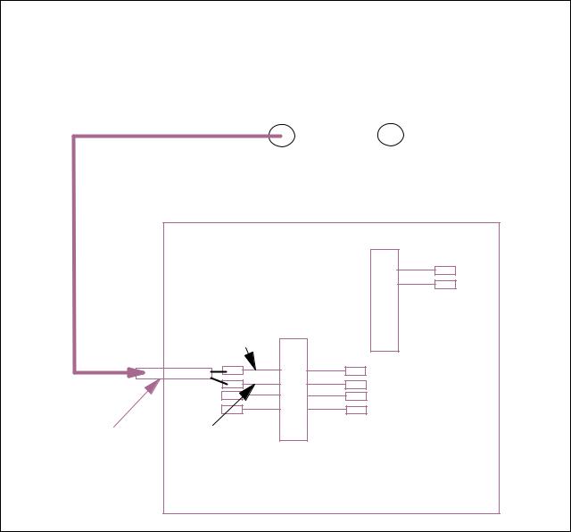
A.1 Figure A.1 shows an example of a typical test equipment setup for loop inductance measurements including the equipment, cables, probes, and fixture.
|
Vector Network |
Port 1 Test cable |
Analyzer |
|
|
|
|
short circuit
fixture driven line reference
structure
probe |
return path |
|
connector
Figure A.1 - Example of test equipment setup for loop inductance measurements

EIA-364-109
Page A-2
A.2 Figure A.2 shows an example of the measurement set up for measuring the loop inductance of a fixture with a ground plane return path. The signal and ground vias are shorted together with a copper surface. The test fixture should be designed such that the signal trace, pad interface, and copper surface provide the lowest inductance path from the probe tip to the signal and ground vias. This reference trace and pad interface should represent the same structures and geometries that will be used for the specimen measurement.
Figure A.2 - Example of fixture loop inductance measurement setup

EIA-364-109
Page A-3
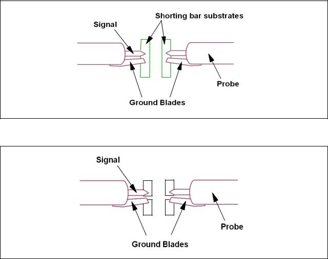
A.3 Figure A.3 shows an example of the measurement set up for measuring the loop inductance of the fixture plus specimen. The figure shows an example of the probe, pads, shorting block, and a specimen consisting of an edgecard connector. The ground pad is connected to the test board ground plane (not shown) that is in turn connected to the specimen ground contacts. It is important that the shorting block connect the specified return path conductors, but not adjacent signal pins.
Figure A.3 - Example of loop inductance measurement setup

EIA-364-109
Page A-4
A.4 Figure A.4 shows a drawing of a microprobe contacting the bottom side of the PCB test fixture and the specimen mounted on the opposite side of the PCB. The test professional should be aware that this type of fixture may be used, but that all vias and traces should be taken into consideration when conducting the calibration procedures.
Microprobe
Fixture
Specimen
Figure A.4 - Diagram of microprobes contacting the bottom side of the printed circuit board test fixture
EIA-364-109
Page B-1
B Calibration standards and test board reference traces (informative)
B.1 Calibration standards
B.1.1 For the equipment calibration, a traceable calibration impedance standard should be used for a reference baseline. Specific equipment calibration should be performed according to the manufacturer’s instructions. However, care should be taken as to what standards or other fixtures are used for the calibration procedure.
NOTE The term “calibration” used in this document is not to be confused with the
periodic factory equipment calibration. Calibration is used in the sense of characterizing the
fixture so that when the “fixture plus specimen” measurement is taken, the characteristics of
the specimen alone can be accurately determined.
B.1.2 When possible the fixture should be designed to allow the attachment of the calibration standard as close to the specimen as possible. Reflections from fixture imperfections increase measurement error.
B.1.3 Printed circuit test boards should not be used as calibration standards. Because of different printed circuit board technologies, fabrication control, and material variations, it becomes difficult to insure that different board designs or fabrication techniques will have the same calibration reference for the impedance measurements. The impedance value of “controlled impedance traces” on a printed circuit board is typically ± 10% or ± 5% of the target value. In measurements and applications, this may be an acceptable tolerance to hold, however, for calibration purposes, this should not be used as a baseline.
B.1.4 The use of the traceable standard termination at the end of the test cable will allow the test fixture printed circuit board effects to be measured more accurately. The test professional will be able to accurately measure the impedance or transmission characteristic of the printed circuit board fixture, and not allow the test equipment to try to compensate for any fixture discontinuities.
B.1.5 Figures B.1 through B.4 show single ended test boards using SOLT (Short-Open-Load-Through) calibration trace structures. Calibration using other methods, for example TRL (Through-Reflect-Line), will require
different structures.
EIA-364-109
Page B-2
Figure B.1 – Short reference trace
Figure B.2 – Open reference trace