

Davis W.A.Radio frequency circuit design.2001
.pdf100 FILTER DESIGN AND APPROXIMATION
C0 |
D |
C |
5.62 |
ωc |
|||
R0 |
D R |
5.63 |
|
Transformation of the low-pass filter to a high-pass filter can be accomplished by another frequency transformation. The normalized complex frequency variable for the low-pass prototype circuit is sn. On the jω-axis the pass band of the low-pass filter occurs between ω D 1 and C1. If the cutoff frequency for the high-pass filter is ωc, then the high-pass frequency variable is
ωc |
5.64 |
s D sn |
Applying this transformation will transform the pass-band frequencies of the lowpass filter to the pass band of the high-pass filter. This is illustrated in Fig. 5.8. The reactance of an inductor, L, in the low-pass filter becomes a capacitance, Ch, in the high-pass filter:
Lsn D |
Lωc |
1 |
5.65 |
|||
|
|
D |
|
|||
s |
Chs |
|||||
or |
|
|
1 |
|
|
|
Ch D |
|
|
|
5.66 |
||
|
|
|||||
Lωc |
||||||
Similarly application of the frequency transformation Eq. (5.64) will convert a capacitor in the low-pass filter to an inductor in the high-pass filter:
1 |
5.67 |
||||||||
|
|
|
Lh D |
|
|||||
Cωc |
|||||||||
jω |
|
|
|
+jω |
|
+jω o |
|||
|
|
|
|||||||
+1j |
|
|
|
|
|
|
|||
|
|
|
|
|
|
||||
|
|
|
|
|
|
|
|||
|
|
|
|
|
|
|
|
|
|
|
|
σ |
|
|
|
σ |
|||
–1j |
|
|
|
|
–j ω |
|
–jω o |
||
|
|
|
|||||||
|
|
|
|
|
|
|
|||
|
|
|
|
|
|
|
|||
|
|
|
|
|
|
|
|
|
|
|
|
|
|
|
|||||
|
|
|
|
|
|
||||
Low pass |
|
High pass |
|||||||
FIGURE 5.8 Low-pass to high-pass transformation.

MATCHING BETWEEN UNEQUAL RESISTANCES |
101 |
A band-pass filter is specified to have a pass band from ω1 to ω2. The “center” of the pass band is the geometric mean of the band edge frequencies, ω0 D pω1ω2. The fractional bandwidth is w D ω2 ω1 /ω0. A band-pass circuit can be formed from the low-pass prototype by using a frequency transformation that will map the pass band of the low-pass filter to the pass band of the band-pass filter. The desired frequency transformation is
sn D |
1 s |
C |
ω0 |
5.68 |
||
w |
|
ω0 |
s |
|||
where s is the frequency variable for the bandpass circuit. To verify this expression for the jω-axis, Eq. (5.58) is rewritten as
1 ω ω0 |
5.69 |
ωn D w ω0 ω |
A short table of specific values for the normalized low-pass prototype circuit and the corresponding band-pass frequencies are shown in Table 5.1.
A graphic illustration of the frequency transformation is shown in Fig. 5.9. A consequence of this transformation is that an inductor L in the low-pass prototype filter becomes a series LC circuit in the band-pass circuit:
Lsn D |
Ls |
C |
Lω0 |
5.70 |
wω0 |
ws |
Similarly a capacitance in the low-pass filter is transformed to a parallel LC circuit:
Csn D |
Cs |
C |
Cω0 |
5.71 |
wω0 |
ws |
Finally, the low-pass to band-stop filter frequency transformation is the reciprocal of Eq. (5.68):
|
s |
|
ω0 |
1 |
sn D w |
|
C |
|
5.72 |
ω0 |
s |
All these transformations from the low-pass prototype filter are summarized in Fig. 5.10.
TABLE 5.1 Low-Pass to Bandpass Mapping
Bandpass ω |
Low-pass ωn |
ω2 |
C1 |
ω0 |
0 |
ω1 |
1 |
ω1 |
C1 |
ω0 |
0 |
ω2 |
1 |

102 FILTER DESIGN AND APPROXIMATION
jω |
+jω |
ω2 |
 ω1
ω1
+1j
σ |
σ |
–1j 
 –ω 1
–ω 1
–jω  –ω 2
–ω 2
Low pass |
Band pass |
FIGURE 5.9 Low-pass to band-pass transformation.
Low pass |
High pass |
Band pass |
Band stop |
||
|
|
|
|
Lw |
|
|
|
|
|
ωo |
|
L |
1 |
L |
w |
|
|
|
|
|
|||
|
ω c L |
ωoW |
Lωo |
1 |
|
|
|
|
|
|
|
|
|
|
|
Lωow |
|
|
|
|
C |
|
|
C |
1 |
ωoW |
1 |
Cw |
|
|
|
||||
ωcC |
|
|
|||
|
|
w |
Cωow |
ωo |
|
|
|
|
|||
|
|
|
|
|
|
|
|
ωoC |
|
|
|
FIGURE 5.10 Filter conversion chart.
5.6.3Chebyshev Bandpass Filter Example
The analytical design technique for a Chebyshev filter with two unequal resistances has been implemented in the program called CHEBY. As an example of its use, we will consider the design of a Chebyshev filter that matches a 15 to a 50 load resistance. It will have n D 3 poles, center frequency of 1.9 GHz, a fractional bandwidth w D f2 f1 /f0 D 20%. The program CHEBY is used

MATCHING BETWEEN UNEQUAL RESISTANCES |
103 |
to find the filter circuit elements. The program could have used the Darlington procedure described in Section 5.6.1, but instead it used the simpler analytical formulas [1]. The following is a sample run of the program:
Generator AND Load resistances |
15.,50. |
|
|||||
Passband ripple |
(dB) |
0.2 |
|
|
|
|
|
Bandpass Filter? |
hY/Ni |
Y |
|
|
hA/Ni |
|
|
Specify stopband attenuation OR n, |
N |
||||||
Number of transmission poles n = |
3 |
|
|
||||
L(1) = |
.62405E + 02 |
C(2) = |
.25125E — 01 |
L(3) = |
.36000E + 02 |
||
Number of poles = 3 Ripple = |
.20000E + 00 dB |
|
|||||
Center Frequency, Fo (Hz), AND Fractional Bandwidth, |
|||||||
w |
1.9E9,.2 |
|
|
|
|
|
|
Through series LC. L1( 1) = |
.261370E — 07 C1( 1) |
||||||
=.268458E — 12
L 1 |
C 1 |
|
L 3 |
C 3 |
R G |
C 2 |
L 2 |
|
R L |
FIGURE 5.11 A 15 : 50 Ohm Chebyshev band-pass filter, where L1 D 26.14 nH, C1 D 0.2685 pF, L2 D 0.6668 nH, C1 D 10.52 pF, L3 D 15.08 nH, and C3 D 0.4654 pF.
Amplitude, dB
0.00
–5.00
–10.00
–15.00
–20.00
–25.00
–30.00 |
1.5 |
1.6 |
1.7 |
1.8 |
1.9 |
2.0 |
2.1 |
2.2 |
2.3 |
2.4 |
1.4 |
Frequency, GHz
FIGURE 5.12 SPICE analysis of a Chebyshev filter.

104 FILTER DESIGN AND APPROXIMATION
Shunt parallel LC. L2( 2) = .666805E — 09 C2( 2)
=.105229E — 10
Through series LC. L3( 3) = .150777E — 07 C3( 3)
=.465370E — 12
The resulting circuit shown in Fig. 5.11 can be analyzed using the SPICE
template described in Appendix G. The results in Fig. 5.12 show |
that the |
||
minimum loss in the pass band is 1.487 dB, which corresponds to |
p |
|
|
H0 |
|||
0.7101. |
|
|
|
PROBLEMS
5.1Design a band-pass filter with center frequency 500 MHz, fractional bandwidth w D 5%, and pass band ripple of 0.1 dB. The out-of-band attenuation is to be 10 dB 75 MHz from the band edge. The terminating impedances are each 50 . Using SPICE, plot the return loss (reflection coefficient in dB) and the insertion loss over the pass band.
5.2Design a band-pass filter with center frequency 500 MHz, fractional bandwidth w D 5%, and pass band ripple of 0.1 dB. The out-of-band attenuation is to be 10 dB 75 MHz from the band edge, and it is to transform a 50 source impedance to a 75 load impedance. Using SPICE, plot the return loss (reflection coefficient in dB) and the insertion loss over the pass band.
5.3Design an elliptic function filter with the same specifications as in Problem 5.1, and plot the results using SPICE.
5.4Design a high-pass three-pole Butterworth filter with cutoff frequency of 900 MHz.
REFERENCES
1.W.-K. Chen, Passive and Active Filters, New York: Wiley, 1986.
2.E. A. Guillemin, Synthesis of Passive Networks, New York: Wiley, 1957.
3.F. F. Kuo, Network Analysis and Synthesis, New York: Wiley, 1962.
4.A. Zverev, Handbook of Filter Synthesis, New York: Wiley, 1967.
5.H. Howe, Stripline Circuit Design, Norwood, MA: Artech House, 1974.

Radio Frequency Circuit Design. W. Alan Davis, Krishna Agarwal
Copyright 2001 John Wiley & Sons, Inc.
Print ISBN 0-471-35052-4 Electronic ISBN 0-471-20068-9
CHAPTER SIX
Transmission Line Transformers
6.1INTRODUCTION
The subject matter of Chapter 3 was impedance transformation. This subject is taken up here again, but now with more careful attention given to the special problems and solutions required for RF frequency designs. The discrete element designs described previously can be used in RF designs with the understanding that element values will change as frequency changes. The alternative to discrete element circuits are transmission line circuits. The classical microwave quarter wavelength transformer can be used up to hundreds of GHz in the appropriate transmission line medium. However, at 1 GHz, a three-section quarter wavelength transformer would be a little less than a meter long! The solution lies in finding a transformation structure that may not work at 100 GHz but will be practical at 1 GHz.
The conventional transformer consists of two windings on a high-permeability iron core. The flux, , is induced onto the core by the primary winding. By Faraday’s law the secondary voltage is proportional to d /dt. For low-loss materials, the primary and secondary voltages will be in phase. Ideal Transformers have perfect coupling and no losses. The primary-to-secondary voltage ratio is equal to the turns ratio, n, between the primary and secondary windings, namely Vp/Vs D n. The ratio of the primary to secondary current is Ip/Is D 1/n. This implies conservation of power, VpIp D VsIs. As a consequence the impedance seen by the generator or primary side in terms of the load impedance is
ZG D n2ZL
When the secondary side of the ideal transformer is an open circuit, the input impedance of the transformer on the primary side is 1.
In a physical transformer the ratio of the leakage inductances on primary and secondary sides is Lp/Ls D n. For the ideal transformer, Lp and Ls approach
105

106 TRANSMISSION LINE TRANSFORMERS
1, but their ratio remains finite at Lp/Ls D n. The physical transformer has an associated mutual inductance, M D k LpLs, where k is the coupling coefficient. The leakage inductance together with the interwire capacitances limits the highfrequency response. The transmission line transformer avoids these frequency limitations.
6.2IDEAL TRANSMISSION LINE TRANSFORMERS
It was found earlier, in Chapter 2, that inductive coils always come with stray capacitance. It was this capacitance that restricted the frequency range for a standard coupled coil transformer. The transmission line transformer can be thought of as simply tipping the coupled coil transformer on its side. The coil inductance and stray capacitance now form the components for an artificial transmission line whose characteristic impedance is
Z0 D |
L |
6.1 |
C |
The transmission line can be used, in principle, up to very high frequencies, and in effect it reduces the deleterious effects of the parasitic capacitance. The transmission line transformer can be made from a variety of forms of transmission lines such as a two parallel lines, a twisted pair of lines, a coaxial cable, or a pair of wires on a ferrite core. The transmission line transformer can be defined as having the following characteristics:
1.The transmission line transformer is made up of interconnected lines whose characteristic impedance is a function of such mechanical things as wire diameter, wire spacing, and insulation dielectric constant.
2.The transmission lines are designed to suppress even mode currents and allow only odd-mode currents to flow (Fig. 6.1).
3.The transmission lines carry their own “ground,” so transmission lines relative to true ground are unintentional.
4.All transmission lines are of equal length and typically < /8.
5.The transmission lines are connected at their ends only.
6.Two different transmission lines are not coupled together by either capacitance or inductance.
io |
ie |
io |
ie |
|
|
FIGURE 6.1 A two-wire transmission line showing the oddand even-mode currents.

IDEAL TRANSMISSION LINE TRANSFORMERS |
107 |
7.For a short transmission line, the voltage difference between the terminals at the input port is the same as the voltage difference at the output port.
Some explanation of these points is needed to clarify the characteristics of the transmission line transformer. In property 2, for a standard transmission line the current going to the right must be equal to the current going to the left in order to preserve current continuity (Fig. 6.1). Since only odd-mode currents are allowed, the external magnetic fields are negligible. The net current driving the magnetic field outside of the transmission line is low. The third point is implied by the second. The transmission line is isolated from other lines as well as the ground. The equality of the odd mode currents in the two lines of the transmission line as well as the equivalence of the voltages across each end of the transmission line is dependent on the transmission line being electrically short in length. The analysis of transmission line transformers will be based on the given assumptions above.
As an example consider the transmission line transformer consisting of one transmission line with two conductors connected as shown in Fig. 6.2. The transformation ratio will be found for this connection. Assume first that v1 is the voltage across RG and i1 is the current leaving the generator resistance:
1.i1 is the current through the upper conductor of the transmission line.
2.The odd-mode current i1 flows in the opposite direction in the lower conductor of the transmission line.
3.The sum of the two transmission line currents at the output node is 2i1.
4.The voltage at the output node is assumed to be vo. Consequently the voltage at left side of the lower conductor in the transmission line is vo above ground.
5.On the left-hand side, the voltage difference between the two conductors is v1 vo.
|
1 i1 |
5 |
2i1 3 |
|
v1 |
vo |
|
RG |
4 vo |
0 |
i1 |
i1 |
2 |
RL |
|
|
|
FIGURE 6.2 Analysis steps for a transmission line transformer.

108 TRANSMISSION LINE TRANSFORMERS
This is the same voltage difference on the right hand side. Consequently,
vo 0 D v1 vo
vo D v1
2
If RG D v1/i1, then
RL D |
vo |
D |
v1/2 |
D |
RG |
6.2 |
2i1 |
2i1 |
4 |
This 4 : 1 circuit steps down the impedance level by a factor of 4.
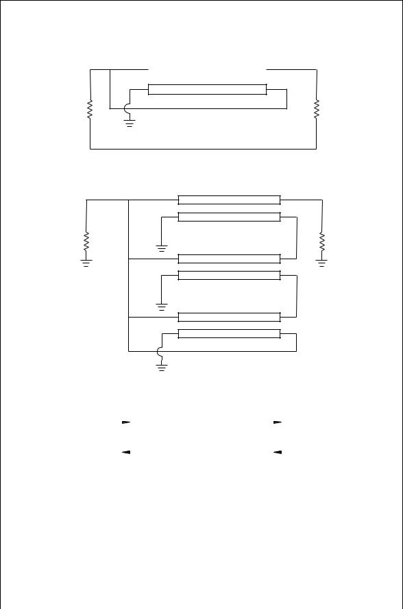
A physical connection for this transformer is shown in Fig. 6.3 where the transmission line is represented as a pair of lines. In this diagram the nodes in the physical representation are matched to the corresponding nodes of the formal representation. The transmission line is bent around to make the B–C distance a short length. The transmission line, shown here as a two-wire line, can take a variety of forms such as coupled line around a ferromagnetic core, flexible microstrip line, or coaxial line. If the transformer is rotated about a vertical axis at the center, the circuit shown in Fig. 6.4 results. Obviously this results in a 1 : 4 transformer where RL D 4RG. Similar analysis to that given above verifies this result. In addition multiple two-wire transmission line transformers may be tied together to achieve a variety of different transformation ratios. An example of three sections connected together is shown in Fig. 6.5. In this circuit the current from the generator splits into four currents going into the transmission lines. Because of the equivalence of the odd-mode currents in each line, these four currents are all equal. The voltages on the load side of each line pair build up from ground to 4 ð the input voltage. As a result, for match to occur, RL D 16RG.
The voltages and currents for a transmission line transformer (TLT) having a wide variety of different interconnections and numbers of transmission lines can
|
A |
C |
|
B |
|
B |
|
|
A |
C |
|
|
|
D |
|
D |
|
(a) |
|
(b) |
FIGURE 6.3 A physical two-wire transmission line transformer and the equivalent formal representation.
IDEAL TRANSMISSION LINE TRANSFORMERS |
109 |
|
|
|
|
|
|
|
RG |
RL |
FIGURE 6.4 An alternate transmission line transformer connection.
RG RL
FIGURE 6.5 A 16 : 1 transmission line transformer.
|
xV |
yV |
|
|
|
||
|
|
TLT |
|
|
yI |
xI |
|
|
|
|
|
|
|
|
|
FIGURE 6.6 Symbol for general transmission line transformer.
be represented by the simple diagram in Fig. 6.6 where x and y are integers. The impedance ratios, RG D x/y2RL, range from 1 : 1 for a one-transmission line circuit to 1 : 25 for a four-transmission line circuit with a total of 16 different transformation ratios [1]. A variety of transmission line transformer circuits are found in [1] and [2].