

диафрагмированные волноводные фильтры / 0b4e957e-43f1-497d-8dd8-13dcc5516faa
.pdfAn approach to filter-antenna integration in SIW technology
Omar A. Nova, Juan C. Bohórquez, and Néstor M. Peña, Member, IEEE
University of Los Andes, Department of Electrical and Electronic Engineering, Bogotá, Colombia
Abstract — An original filter-antenna module has been designed, manufactured and measured. The module can be viewed as a high order filter in which the last resonator has been replaced by a resonant antenna element. This antenna is coupled to the other resonators by means of two inter-cavity slots. The module was manufactured using the Substrate Integrated Waveguide technique, which allows the cavities to be fabricated by means of a standard printed circuit board process. Experimental results present good agreement with simulations. The measured return loss response of the filter-antenna module matches that of a second order bandpass filter, with a central frequency of 1.94GHz, a fractional bandwidth of 5.15% and a return loss of 7.5dB at the central frequency. The radiation function is incorporated to this filter’s response, with a maximum gain of 5.15dBi and a front-to-back ratio (FTBR) of 29.25dB.
Index Terms — Bandpass filters, cavity resonator filters, slot antennas, substrate integrated waveguide.
I. INTRODUCTION
The trend of communications systems has lead designers to require light weight, robustness and easy integration with planar circuits [1]. Thus, technologies such as Substrate Integrated Waveguide (SIW) emerge as an option to develop the communication systems that fit the imposed restrictions.
The SIW technique makes possible to put together volume structures with planar ones within a circuit fabricated by means of conventional planar processes such as printed circuit board (PCB) or low-temperature co-fired ceramic (LTCC) [2]. This technique consists of fabricating waveguide-like structures in planar form by implementing the lateral walls as arrays of metalized holes.
Using the SIW technology, different contributions have been reported for filters and antennas. The SIW filter’s topology explored in [3] consists of the coupling of side-by- side horizontally oriented SIW cavities by means of evanescent waveguide sections. Antennas were integrated as open-end waveguide radiators or waveguide slot antennas [4]. Recently, in [5] a SIW cavity-backed antenna has been presented, in which the properties of the TE101 mode are exploited to obtain the smallest possible cavity, lower power loss and an antenna layout that fits within the surface cavity area.
In order to increase the compactness of the RF front-end of a communication system, integrating both the filtering and the radiation functions in just one module has been proposed . Several approaches have been reported regarding the integration of a filter with an antenna. In [6] a filter-antenna is
obtained for a central frequency (f0) of 10GHz, by integrating the filtering function in an electromagnetic horn antenna by means of the introduction of some metallic posts inside the antenna. The reported return loss is greater than 11dB and the -3dB fractional bandwidth is 9.8%. In [7], the integration filter-antenna is obtained by covering a horn antenna’s aperture with frequency selective surfaces implemented with SIW cavities (SIWC-FSS). This solution presents f0=9.8GHz, return loss greater than 17dB and a -3dB fractional bandwidth of 14.28%.
Some planar approaches have been proposed to achieve the filter-antenna integration as is described in [8]. The idea consists of the integration of a slot antenna as the third resonator of a second order bandpass filter conformed by the combination of two resonators implemented in thin film microstrip lines (TFMS) and coupled by admittance inverters in coplanar waveguide (CPW). The obtained filter-antenna response has a return loss greater than 12dB with a -3dB fractional bandwidth of 18.38%.
In this paper, a bandpass filter-antenna module for f0=2GHz is obtained by coupling two SIW cavities. One of these cavities contains a cavity-backed slot antenna and is integrated as the second resonator of the designed second order filter-antenna module. The other cavity, apart from being the first resonator, has the input coupling network of the circuit. In this way, a completely integrated SIW filterantenna module is achieved.
II. CAVITY-BACKED ANTENNA
The guided modes in a SIW structure are TEn0 modes [2]. Then, we focus on the design of the cavity for this kind of modes. In order to select which TEn0 mode to excite, the miniaturization of the structure is taken into account. For this reason, the TE10 mode is chosen, as it permits the minimization of the cavity’s width, a (Fig. 1).
Fig. 1. Geometry and spatial disposition of the designed cavity.
978-1-4244-9485-9/11/$26.00 ©2011 IEEE

The TE101 mode is chosen as the cavity’s resonance mode because it enables the reduction of the power lost in the cavity’s metallic walls (Pc), compared with the other TE10L modes. Finally, the cutoff frequency, fc-TE10, was defined in order to obtain the greatest possible separation from higher order resonances as in [5]. The cutoff frequency that enables the fulfillment of this condition is fc-TE10=1.41GHz. It also can be shown that for this value of fc-TE10, the cavity results to be square, that is, a=d (Fig. 1).
Having selected the resonance mode TE101, the cutoff frequency fc-TE10=1.41GHz and the resonant frequency f0=2GHz, the cavity’s dimensions are calculated to be a=d=71.5mm, while h=1.57mm=thickness of substrate [9].
The antenna layout is obtained as described in [5]. This leads to an antenna consisting of two meandered slots of length /2 with their common origin point placed at the point of maximum electric current. In this way, the two electric current components necessary for the accomplishment of a slot antenna are established: the circulating component, responsible for the resonant condition and the perpendicular component, responsible for the radiation. The structure of the antenna obtained is presented in Fig. 2.
Fig. 2. 3D-view of the SIW cavity-backed slot antenna designed to be integrated within the SIW filter-antenna module.
III. FILTER-ANTENNA MODULE
A. Access line
The access line can be observed in the circuit of Fig. 3. The energy is coupled to the cavity by means of the input-output magnetic coupling slots that are located in the upper face of the cavity at an approximate distance of λg/8 from the edge. They are designed according to the procedure described in [10]. A coplanar waveguide feeding structure is shortcircuited in the middle of the coupling slots, guaranteeing a maximum current density in the slot regions for the different frequencies of resonance, enhancing optimal magnetic coupling conditions to the cavity.
B. Inter-cavity coupling
The topology used to couple the two SIW cavities consists of placing them in vertical orientation with a top-to-bottom configuration, as it is shown in Fig. 3. The inter-cavity coupling is obtained by means of two slots placed at the shared metallization.
Fig. 3. SIW filter-antenna module’s topology
The coupling between cavities was designed to guarantee the following two conditions:
1)The field distribution shown in Fig. 4, around the meandered slot of the cavity-backed antenna presented in Section II, must be kept.
2)The two cavities must be coupled to obtain a bandpass filter response.
(a) (b)
Fig. 4. Magnitude distribution of E and H fields over the ground plane around the meandered slots, for the designed SIW cavitybacked slot antenna. (a) E-field. (b) H-field.
The inter-cavity coupling with slots was initially conceived in order to fulfill the first coupling condition. For that reason, the short ends of the meandered and the coupling slots were made to match up. This configuration allows the establishment of a current maximum at the point where the ends of the two meandered slots coincide (Fig. 5). It is because the current flows around the end of the slot at a short end of a slot line. Additionally, in order to obtain the fields distribution of Fig. 4, the coupling slots’ lengths were set as large as possible with the intention of placing the maximums
of the H-field at the two ends of both meandered slots, as showed in Fig. 6. At the same time, with these slots’ dimensions, the maximums of the E-field are obtained at the middle of each meandered slot, as intended (Fig. 6).
(a) |
(b) |
Fig. 5. Distribution of electric |
current over the ground plane |
around the meandered slots of the SIW filter-antenna module. (a) Current lines. (b) Current magnitude.
TABLE I
PHYSICAL DIMENSIONS OF THE SIW FILTER-ANTENNA MODULE (mm)
a |
77.5 |
d |
77.5 |
wm |
4.82 |
lm |
39.8 |
wc |
2.4 |
dc |
3.1 |
d1 |
23 |
w1 |
2.8 |
l1 |
28 |
w2 |
5 |
l2 |
34 |
d2 |
32 |
s1 |
2.5 |
s2 |
3.5 |
x1 |
6.2 |
x2 |
8.2 |
x3 |
8.2 |
x4 |
8.2 |
x5 |
10.8 |
y1 |
15.1 |
y2 |
13.3 |
y3 |
11.5 |
y4 |
15.1 |
w3 |
1.8 |
d3 |
24.8 |
s3 |
2.4 |
s4 |
12 |
s5 |
11 |
IV. EXPERIMENTAL RESULTS
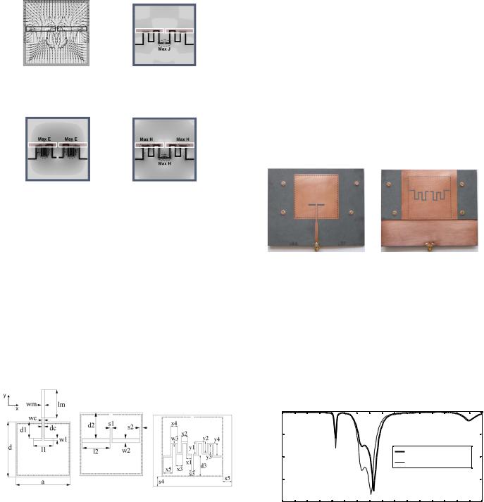
The designed SIW filter-antenna module was fabricated by means of a standard PCB process on two plates of Rogers RT/duroid 5880 substrate ( r=2.2, tan =0.0009, h=1.57mm). The two plates were used to separately implement the top and the bottom cavities, attached by means of four screws, as is shown in Fig. 8. Two photographs of the built SIW filterantenna module are presented in Fig. 8.
(a) (b)
Fig. 6. Magnitude distribution of E and H fields over the ground plane around the meandered slots, for the designed SIW filterantenna module. (a) E-field. (b) H-field.
To fulfill the second coupling condition, the position of the two coupling slots was changed. By means of full wave simulations in High-Frequency Structure Simulator (HFSS), an optimization process was executed over this variable in order to obtain the value of the coupling coefficient (kx) that allows achieving a second order bandpass filter response.
Finally, the metallic layers of the SIW filter-antenna module are presented in Fig. 7. It can be observed that, for measurement convenience, a 50 microstrip line was attached to the CPW line. The transition between the two widths of the strip conductors was optimized to accomplish the required input coupling. Physical dimensions of the filter-antenna module are listed in Table I.
(a) |
(b) |
(c) |
Fig. 7. Metallic layers of the SIW filter-antenna module. (a) Top metallization. (b) Inter-cavity metallization. (c) Bottom metallization.
(a) (b)
Fig. 8. Photographs of the built SIW filter-antenna module. (a) Top view. (b) Bottom view.
Fig. 9 shows the S11 parameter of the filter-antenna module. Despite a return loss difference of 4.8dB at central frequency, a good agreement between experimental and simulated results was obtained. The return loss difference is due to a coupling problem originated by technological defaults, mainly by a misalignment between the two cavities. The experimental central frequency of 1.94GHz and -3dB fractional bandwidth of 5.15%. are quite similar to those obtained by electromagnetic simulations (f0=1.93GHz, -3dB-BW=5.18%).
(dB) |
0 |
|
|
|
|
|
|
|
|
-5 |
|
|
|
|
|
|
|
|
|
parameter |
|
|
|
|
|
|
|
|
|
-10 |
|
|
|
|
Measurement |
|
|||
|
|
|
|
HFSS simulation |
|
||||
|
|
|
|
|
|
||||
-15 |
|
|
|
|
|
|
|
|
|
S11 |
|
|
|
|
|
|
|
|
|
|
|
|
|
|
|
|
|
|
|
|
-20 |
1,7 |
1,8 |
1,9 |
2 |
2,1 |
2,2 |
2,3 |
2,4 |
|
1,6 |
||||||||
Frequency (GHz)
Fig. 9. Measured and simulated S11 parameter of the SIW filterantenna module.

The measurement of the SIW filter-antenna module’s radiation patterns was carried out in the anechoic chamber of Los Andes University. Fig. 10 shows the co-polarized radiation patterns at f0=1.94GHz, both in E-plane and in H- plane. The patterns are presented normalized to the maximum measured gain of 5.15dBi. The measured front-to-back ratio (FTBR) was 29.25dB. The experimental results are in agreement with those obtained from electromagnetic simulations.
|
90 |
0 |
|
120 |
90 |
0 |
60 |
120 |
|
60 |
|
||||
|
|
-10 |
|
|
|
-10 |
|
150 |
|
-20 |
30 |
150 |
|
-20 |
30 |
|
-30 |
|
|
-30 |
|
||
180 |
|
|
0 180 |
|
|
0 |
|
210 |
|
|
330 |
210 |
|
|
330 |
240 |
|
|
300 |
240 |
270 |
300 |
|
270 |
|
|
|
|
|||
Measurement |
|
HFSS simulation |
Measurement |
|
HFSS simulation |
||
|
(a) |
|
|
(b) |
|
||
Fig. 10. Measured and simulated co-polarized radiation patterns at f0=1.94GHz. (a) E-plane (yOz plane). (b) H-plane (xOz plane).
The measured co-polarized and cross-polarized radiation patterns at f0=1.94GHz, both in E-plane and in H-plane, are compared in Fig. 11. The maximum measured crosspolarization gain in E-plane is -7.96dBi while in H-plane is -6.40dBi. It results in a co-to-cross polarization ratio of 13.11dB for the E-plane and of 11.55dB for the H-plane.
|
90 |
|
90 |
|
|
120 |
60 |
||
120 |
60 |
|||
|
|
|
10 |
|
|
|
10 |
|
|
|
|
150 |
0 |
30 |
|
150 |
0 |
|
30 |
|||
|
-10 |
|
|
|
|
-10 |
|
-20 |
|
|
|
|
-20 |
180 |
|
|
0 |
180 |
|
0 |
210 |
|
|
330 |
210 |
|
330 |
|
240 |
300 |
|
|
240 |
300 |
|
270 |
|
|
|
|
270 |
|
Co-pol |
X-pol |
|
|
|
Co-pol X-pol |
|
(a) |
|
|
|
|
(b) |
Fig. 11. Measured co-polarized and cross-polarized radiation patterns at f0=1.94GHz. (a) E-plane (yOz plane). (b) H-plane (xOz plane).
V. CONCLUSION
In this paper, an original filter-antenna module was presented. This module exhibits a real filter-antenna integration, given that the antenna is one of the filter’s resonators. This
integration can be seen as a contribution to greater compactness of the RF front-end. The antenna integrated within the module can be independently designed at the beginning of the process and then incorporated with the proper design of the coupling between resonators. The correspondence of some module’s physical parameters with the external quality factors (Qe) and the coupling coefficient (kx) must be investigated. The characterization of Qe and kx as a function of the above-mentioned physical parameters is currently being developed by the authors. The design principles presented here are readily applied to obtain an nth order SIW filter-antenna module.
REFERENCES
[1]G. Q. Luo, Z. F. Hu, L. X. Dong, and L. L. Sun, “Planar slot antenna backed by substrate integrated waveguide cavity”,
IEEE Antennas and Wireless Propagation Letters, vol. 7, pp. 236-239, 2008.
[2]F. Xu, and K. Wu, “Guided-wave and leakage characteristics of Substrate Integrated Waveguide”, IEEE Transactions on Microwave Theory and Techniques, vol. 53, No. 1, pp. 66-73, January 2005.
[3]X. Chen, W. Hong, T. Cui, J. Chen, and K. Wu, “Substrate Integrated Waveguide (SIW) linear phase filter”, IEEE Microwave and Wireless Components Letters, vol. 15, No. 11, pp. 787-789, November 2005.
[4]S. Yang, A. Elsherbini, S. Lin, A.E. Fathy, A. Kamel, and H. Elhennawy, “A highly efficient Vivaldi antenna array design on thick substrate and fed by SIW structure with integrated GCPW feed”, IEEE Antennas and Propagation International Symposium, pp. 1985-1988, June 2007.
[5]J.C. Bohórquez, H.A. Forero, I.C. Herrera, J. Avella, N. Peña, and H.F. Guarnizo, “Planar Substrate Integrated Waveguide cavity-backed antenna”, IEEE Antennas and Wireless Propagation Letters, vol. 8, pp. 1139-1142, 2009.
[6]B. Froppier, Y. Mahé, E. M. Cruz, and S. Toutain, “Integration of a filtering function in an electromagnetic horn”, 33rd European Microwave Conference, vol. 3, pp. 939-942, October 2003.
[7]G. Q. Luo, W. Hong, H. J. Tang, J. X. Chen, X. X. Yin, Z. Q. Kuai, and K. Wu, “Filtenna consisting of horn antenna and Substrate Integrated Waveguide Cavity FSS”, IEEE Transactions on Antennas and Propagation, vol. 55, No. 1, pp. 92-98, January 2007.
[8]T. Le Nadan, J.P. Coupez, S. Toutain, and C. Person, “Integration of an antenna/filter device, using a multi-layer, multi-technology process”, 28th European Microwave Conference, vol. 1, pp. 672-677, October 1998.
[9]D.M. Pozar, Microwave Engineering, New York: J. Wiley & Sons, 2005.
[10]J.C. Bohórquez, Contribution a la conception de filtres reconfigurables sur la base de technologies planaires et SIW,
Thesis to obtain the doctor degree, Brest, L’École Nationale Supérieure des Télécommunications de Bretagne, 2007.