

диафрагмированные волноводные фильтры / 5ae274f5-adee-4a89-9a8e-78dfef57c204
.pdfTunable
SIW Structures
Kamran Entesari, Alireza Pourghorban Saghati,
Vikram Sekar, and Marcelino Armendariz
Developing radio-frequency (RF), microwave, and millimeter-wave systems requires low-cost, mass-produc- ible, high-performance, and high-yield technologies for passive and active
sections. Dealing with radio coexistence and strong coupling between different subsystems while maintaining or even reducing the size and weight of the final system is a very challenging task. This is more important when designing passive circuits such as resonators, antennas, highly selective filters, couplers, power dividers, and circulators [1], [2]. Classical waveguide technology was, and in some cases still is, the mainstream for designing high-performance passive circuits and systems [3], [4]. However, these bulky and heavy concomitants are not suitable for integration and low-cost mass production. Via posts were first used under the name laminated waveguides [5] in 1998 and as a subset of substrate integrated circuits [6] in
2001 to form a planar waveguide structure. Then, by the introduction of the substrate integrated waveguide (SIW) technology as we know it today by Deslandes and Wu [7], a remedy for the full integration of active and passive circuits in a planar fashion was found [7]– [11]. Using this method, a nonplanar rectangular waveguide can be made in a planar form that is compatible with the existing printed circuit board (PCB) and lowtemperature cofired ceramic techniques [12]. Conductive walls in classical waveguides are replaced with planar-compatible PCBs via posts in SIW structures. Similar to classical metallic waveguides, by shortening the two openings of the SIW structure at both ends, SIW cavities can also be formed.
High-Q resonators are a typical part of many highperformance passive and active circuits. As a result, an SIW is a very good candidate for developing planar microwave devices with high quality factors. SIW technology has been applied to many microwave
Kamran Entesari (kentesar@ece.tamu.edu) and Alireza Pourghorban Saghati (saghati@tamu.edu) are with the Electrical and Computer Engineering Department, Texas A&M University, College Station, United States. Vikram Sekar (vikram_sekar@ieee.org) is with Peregrine Semiconductor Corp., San Diego, California, United States. Marcelino Armendariz (marcelino.armendariz@raytheon.com) is with Raytheon Company, Dallas, Texas, United States.
Digital Object Identifier 10.1109/MMM.2015.2408273
Date of publication: 7 May 2015
34 |
1527-3342/15©2015IEEE |
June 2015 |

components, such as post and cavity filters [9], [13], [14], antennas [15], [16], directional couplers [17], oscillators [18], [19], power amplifiers [20], [21], slot array and leaky-wave antennas [22]–[24], and circulators [25]. Devices realized using SIWs preserve most of the advantages of conventional metallic waveguides. Some of the advantages are
1)low loss and high quality factor for SIW cavities
2)permanent electrical isolation due to the shielding via posts
3)high-power handling
4)integrability capabilities of SIW structures with all sorts of passive and active components.
The first two items have been proven to be as good as classical metallic waveguides, but the third advantage may be hindered to some extent in SIWs. Based on the dielectric material used in the PCB fabrication process and the height of the dielectric layer, the power-han- dling capabilities of the SIW structure can be reduced. While the first three advantages are the intrinsic properties of three-dimensional (3-D) waveguide structures, the integratability capability is an advantage that SIWs inherit from planar structures. In other words, an SIW has the benefits of both 3-D and planar microwave structures in one place.
Why Tunable SIW
Like almost all the resonance-based microwave structures offering a quality factor in the range of a couple of hundred, this high quality factor comes along with a narrow bandwidth (BW). Although this is very helpful in designing highly selective microwave devices for a particular center frequency, sometimes covering a wider BW is needed.
Even in narrowband applications, due to the high sensitivity of the SIW structures (similar to the resonant-based classical metallic cavity structures), postfabrication tuning of the fabricated device is mandatory in most cases to fine-tune the device’s operating frequency to the desired frequency response. Otherwise, corrective refabrication of the device is inevitable. Unlike multiple/wideband microwave devices, tunable structures offer better isolation. It is true that multifrequency structures have the advantage of serving multiple frequencies at the same time, but the crosstalk from neighbor bands makes them a poor choice in comparison with tunable/reconfigurable devices [26]–[28]. Covering multiple bands should not decrease the selectivity and Q of the device, which is not true for multifrequency structures. Based on the previously given information and that provided in [8]–[13], [15]–[23], and [25]–[28], there are
June 2015
Classical waveguide technology was, and in some cases still is, the mainstream for designing high-performance passive circuits and systems.
several known reasons why tuning of SIW devices can be useful.
1)More standards/services can be covered by the same device.
2)Postfabrication fine-tuning of the device becomes possible.
3)Less crosstalk sensitivity (better isolation) can be achieved while covering more bands.
The importance of SIW tuning needs to be discussed for major microwave passive and active devices such as antennas, voltage-controlled oscillators (VCOs), and filters.
SIW Tunable Antennas
There are so many applications in which an antenna needs to be mounted on a conductive surface such as a vehicle, an airplane, or even a human body [29]. Antennas in these cases usually need to be high gain. On the other hand, the increasing number of commercial wireless services comes along with the increased antenna numbers that a user end device needs. The combination of these two points means that antennas must exhibit high gain, be mountable on conductive surfaces, and cover multiple services.
For the first two requirements, the SIW antenna is a very good choice since it has a very high gain and, due to the cavity-backed structure, it can be mounted on almost any surface without affecting its performance [30]. Because of its narrow BW, it may not be a good choice to be used for multiple numbers of services, which is why tunability of the SIW antennas becomes important. The wide-range tuning of the SIW antennas is challenging due to their nature. To achieve a compact structure, most of the antennas presented so far used a cavity operating at its transverse electric (TE) fundamental ^TE101h mode [15], [16], [30], [31]. The resonant frequency of TE101 mode for an SIW cavity with length L and width W can be found using
|
c |
|
1 |
2 |
|
1 |
2 |
|
|
f101 = |
c |
m |
+c |
m , |
(1) |
||||
2 er nr |
Leff |
Weff |
where c is the speed of light in a vacuum and fr and nr are the relative permittivity and permeability of the
35

Tuning a filter is even more challenging than tuning a single resonator structure such as an antenna or a VCO.
substrate used for the SIW cavity, respectively. The values of the effective length and width of the SIW cavity can be found using
|
f0 |
|
|
FOM =-L(Df ) +20 log( |
|
) -10 log(P) |
(4) |
Df |
|||
FOMT =-L(Df ) +20 loge Df0f # FTR10 o -10 log(P), (5)
where L (Df ) is the phase noise at offset Df, f0 is the oscillation frequency, P is the consumed dc power used by the VCO, and FTR is the frequency tuning ratio percentage. The standard FOM for VCOs is shown in (4), and (5) factors in the tuning range as well.
Leff |
= L - |
|
d2 |
|
+0.1 |
d2 |
|
|
(2) |
SIW Tunable Filters |
|
|
|
|||
|
0.95.b |
|
L |
|
|
|
||||||||||
|
|
|
|
|
|
The significant demand for dynamic spectrum man- |
||||||||||
|
|
|
|
|
|
|
|
|
|
|
||||||
and |
|
|
|
|
|
|
|
|
|
|
agement in cognitive and software-defined radios |
|||||
|
|
|
d2 |
|
|
d2 |
|
|
increases the need for RF/microwave devices that |
|||||||
Weff |
= W - |
+0.1 |
, |
(3) |
can operate in different bands [34]–[37]. This means |
|||||||||||
0.95.b |
|
|||||||||||||||
|
|
|
|
|
W |
|
that microwave filters, as one of the major blocks in |
|||||||||
|
|
|
|
|
|
|
|
|
|
|
||||||
respectively [30], where d is the wall vias’ diameter |
designing such systems, need to cover more bands. |
|||||||||||||||
and b is the wall vias’ spacing. Hence, the frequency |
Various solutions for such filters can be employed, |
|||||||||||||||
of operation in a cavity-backed SIW antenna depends |
such as filter banks, multiband filters, and tunable/ |
|||||||||||||||
on both the slot and cavity dimensions. As a result, |
reconfigurable filters. Although filter banks deliver |
|||||||||||||||
conventional tuning methods [28], [32] applied to slot |
a very high-quality performance, a very large area |
|||||||||||||||
antennas are not effective in designing SIW antennas as |
is needed to accommodate them in a system. Mul- |
|||||||||||||||
they only change the slot’s modes. Higher-order modes |
tiband filters suffer from isolation and crosstalk |
|||||||||||||||
are excited in a waveguide cavity and lead to a poor |
problems and, thus, are less appealing compared |
|||||||||||||||
upper-band rejection or the appearance of undesired |
with tunable/reconfigurable filters. The ease of fab- |
|||||||||||||||
resonance frequencies in the tuned states. As a result, |
rication, high-power handling, high linearity, and |
|||||||||||||||
these modes also need to be considered when designing |
integrability of SIW filters with other sections of the |
|||||||||||||||
a tunable SIW antenna. |
|
|
|
|
|
|
|
|
microwave system make them a good candidate for |
|||||||
The resonance frequency of a cavity resonator can |
high-performance microwave circuits. However, due |
|||||||||||||||
be changed by changing its effective length, width, fr, |
to their resonant nature, SIW filters are narrrowband |
|||||||||||||||
and nr, as shown by (1)–(3). However, changing these |
and highly selective. |
|
|
|
||||||||||||
parameters might not be practical. While changing the |
Finding a way to tune SIW-based filters over a wide |
|||||||||||||||
permeability is used in one method, the other methods |
tuning range while maintaining their high Q results |
|||||||||||||||
use field perturbation and reactive loading inside the |
in high-performance, wide-range operating filters. |
|||||||||||||||
cavity to tune the SIW antennas. |
|
However, this has not been the case for most of the |
||||||||||||||
SIW Tunable VCOs |
|
|
|
|
|
|
|
|
proposed tuning methods so far. Either the tuning |
|||||||
|
|
|
|
|
|
|
|
range is very low or the Q of the resonator drops when |
||||||||
VCOs are used as the local oscillator source in most |
a wide tuning range is achieved, making it more chal- |
|||||||||||||||
radar and communication applications [33]. Some of the |
lenging when designing such filters. |
|
||||||||||||||
driving parameters for VCOs are low phase noise, high |
On the other hand, the BW and in-band loss of a |
|||||||||||||||
output power, low dc power, high tuning range, and |
multipole filter are related to the coupling coefficient |
|||||||||||||||
high harmonic suppression. It is well known that the |
and external Q factors. For example, for a two-pole fil- |
|||||||||||||||
performance of a VCO is highly affected by the Q of the |
ter, the required K12 value can be extracted from full- |
|||||||||||||||
passive resonator. |
|
|
|
|
|
|
|
|
wave simulations using [38] |
|
|
|
||||
The high Q, power handling, and isolation of the |
|
|
|
|
|
|||||||||||
SIW cavity resonators in addition to their integrabil- |
2 |
2 |
|
|
||||||||||||
K12 = |
f1 |
-f2 |
, |
(6) |
||||||||||||
ity capabilities sound very promising when designing |
2 |
2 |
||||||||||||||
|
f1 |
+f2 |
|
|||||||||||||
oscillators. However, due to the difficulties in tuning |
|
|
|
|
|
|||||||||||
these structures, they have not been used in VCO struc- |
where f1 and f2 are the two resonant peaks seen in |
|||||||||||||||
tures that often. As a result, a tuning method by which |
S21 simulation results of the cavities coupled to each |
|||||||||||||||
SIW resonators can be tuned over a wide tuning range |
other, also known as oddand even-mode resonance |
|||||||||||||||
while their quality factor variations are negligible is |
frequencies, respectively. |
|
|
|
||||||||||||
very demanding. |
|
|
|
|
|
|
|
|
|
|
The external quality factor (Qe ) can be also extracted |
|||||
To have a fair comparison between different SIW |
using a singly loaded SIW cavity resonator. The Qe can |
|||||||||||||||
VCOs, two figures of merit (FOM) and FOM with tun- |
then be computed from 3-D full-wave simulations and |
|||||||||||||||
ing range (FOMT) are used in this article as |
|
by employing the expression [38] |
|
|||||||||||||
36 |
|
|
|
|
|
|
|
|
|
|
|
|
|
|
June 2015 |
|

f0 |
, |
(7) |
Qe = Df! 90% |
where f0 is the resonance frequency of the SIW cavity resonator and Df! 90% denotes the difference of frequencies of which a phase shift of ! 90c occurs in the S11 response of the cavity resonator.
Equations (6) and (7) show that the coupling coefficient and the external quality factor in a filter change with the frequency. This means that tuning a filter is even more challenging than tuning a single resonator structure such as an antenna or a VCO. As a result, these factors are also important and need to be considered in the design process of a tunable SIW filter.
To address the previously given points in more detail, in this article, we specifically focus on frequency-tun- able/reconfigurable SIW structures. Such RF/microwave devices employ different tuning elements such as posi- tive-intrinsic-negative (p-i-n) diodes, varactor diodes, RFmicroelectromechanical systems (RF-MEMS) switches, and sometimes mechanical contacts to achieve frequency tuning. The following section serves as a detailed overview of all of the tuning techniques used for SIW devices. The basis of each technique, its pros and cons, and the potential applications for each tuning technique are discussed. The detailed libraries of the proposed tunable SIW antennas, VCOs, filters, and other microwave struc-
SIW has the benefits of both 3-D and planar microwave structures in one place.
tures are provided with comparison tables for each at the end of each section.
Tunable SIW Resonators and Fundamental Tuning Methods
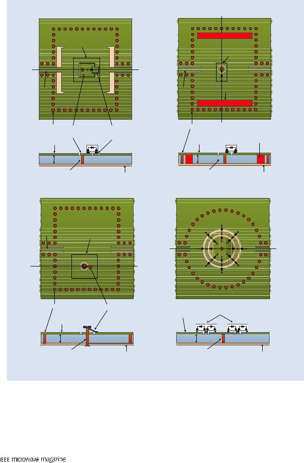
Since SIW antennas, VCOs, and filters are made out of one, two, or more cavity resonators, it is possible to tune these SIW structures by tuning all of the resonators simultaneously. To the best of the authors’ knowledge, six different methods have been reported in the literature to tune SIW resonators. Each technique uses a fundamental tuning element (e.g., a p-i-n diode, a varactor diode, an RF-MEMS switch, ferrite material, or a tuning screw) to tune the resonator and, thus, the final SIW structure. While some methods are based only on changing the electrical characteristics of the cavity resonators, others aim to change both the magnetic and electrical characteristics. A summary of the tuning methods for SIW resonators is presented in the following sections. Figure 1 shows a conceptual description of each tuning method.
|
Electrical Tuning |
|
|
|
|
Element |
|
A |
|
|
Al |
Vtune |
|
|
Top View |
|
|
|
|
Wall Via |
|
|
|
Loading |
|
Cavity |
|
Varactor |
|
Top Wall |
|
A |
|
Al |
View |
h1 |
fr1 |
|
|
|
Side |
||
|
|
|
|
|
|
Cavity |
|
|
|
Bottom Wall |
|
(a)
|
|
Tuning |
|
|
Element |
A |
|
Al |
|
|
w |
Feed Line |
(50 X) |
Top View |
Top Via |
Switching |
Cavity |
Wall Via |
||
Device |
|||||
A |
Top Wall |
|
|
||
|
Al |
View |
|||
|
|
||||
h2 |
|
fr2 |
|||
|
|
||||
h1 |
|
fr1 |
|
Side |
|
Tuning Post |
Cavity |
Cavity |
|
Opening |
Bottom Wall |
|
(b) |
|
Figure 1. (a) The side reactively loaded SIW tunable resonators, (b) the via post-loaded SIW cavity, (c) the floating patch diode-loaded SIW cavity, (d) the ferrite disk-loaded SIW tunable resonator, (e) the mechanically tunable SIW resonators (screwed flap), and (f) the surface ring-gap varactor-loaded SIW cavity. (Continued)
June 2015 |
37 |
|
|
|
|
|
|
|
A |
|
|
Tuning |
|
|
|
|
Ferrite Slab |
|
|
|
|
|
|
|
|
|
||
|
Element |
|
|
|
|
|
|
|
|
|
|
|
|
|
Electrical Tuning Element |
||
A |
|
|
|
Al |
|
|
|
|
CPW-G Line (50X) |
|
|
|
TopView |
CPW-G Line |
Magnetic Tuning Element |
||
|
|
|
(50X) |
Ferrite Slab |
|
|||
|
|
|
|
|
|
|
|
|
Wall Via |
Metallic |
|
Isolated |
|
Wall Via |
Al |
Ferrite |
|
|
|
|
||||||
Cavity |
Patch |
Loading |
Floating Metal |
|
Cavity |
Loading |
||
|
Slab |
|||||||
Top Wall |
|
Varactor |
|
View |
|
Top Wall |
Varactor |
|
A |
|
|
Al |
A |
|
|
Al |
|
|
|
Side |
|
|
|
|||
h1 |
fr1 |
|
|
|
h1 |
fr1 |
|
|
Top View
Side View
Plated Via Hole |
|
Cavity |
|
|
|
|
|
|
|
(c) |
Bottom Wall |
|
|
|
|
CPW Line |
(50 X) |
|
|
G- |
Mechanical Tuning |
||
|
|
Element |
|
A |
|
|
Al |
|
|
|
Top View |
Wall Via |
|
Flap |
|
|
Cavity |
Tuning |
|
|
Top Wall |
Screw |
|
A |
|
Al |
View |
h1 |
fr1 |
|
Side |
|
|
Plated Via Hole |
Cavity |
|
|
|
Bottom Wall |
|
(e) |
Plated Via Hole |
Cavity |
|
Bottom Wall |
|
(d) |
|
A |
Al |
|
|
Top View |
|
Cavity |
Loading Varactors |
|
Top Wall |
||
|
A |
|
Al |
View |
h1 |
fr1 |
|
Side |
|
|
Via Post |
Cavity |
|
|
|
Bottom Wall |
|
(f) |
Figure 1. (Continued) (a) The side reactively loaded SIW tunable resonators, (b) the via post-loaded SIW cavity, (c) the floating patch diode-loaded SIW cavity, (d) the ferrite disk-loaded SIW tunable resonator, (e) the mechanically tunable SIW resonators (screwed flap), and (f) the surface ring-gap varactor-loaded SIW cavity.
Method I |
ity through an opening in one of the side walls. Since |
The tuning method shown in Figure 1(a) was first pro- |
the varactor diode reactive loading effect is applied to |
posed in [39] for a tunable SIW cavity-backed antenna |
the cavity in the area where the E-field distribution is |
oscillator. A varactor diode is coupled to the SIW cav- |
minimum, the tuning achieved using this technique is |
38 |
June 2015 |

not very high (2%), but the Q of the resonator (+286– 299) is affected less in comparison with Methods II–IV.
Method II
The method shown in Figure 1(b) was first proposed by Armendariz et al. [40]. Perturbation of the electric fields inside the cavity is used to change the frequency of the cavity resonator. The method is based on loading the resonator with a via post and then connecting and disconnecting it from the cavity top wall using p-i-n diodes. (A similar method is proposed in [41] using MEMS switches.) By connecting the via post to the top wall, the field distribution inside the cavity is changed. As a result of this manipulation of the fields inside the cavity, the resonance frequency of the resonator is changed. The disconnected via post loads the SIW resonator capacitively, which results in miniaturization of the cavity in the off state. A two-layer structure is employed to switch each tuning via post on or off using p-i-n diodes or RF-MEMS switches. The via post is permanently disconnected from the cavity top wall using a very small opening. The leakage from the opening is negligible and does not affect the Q of the resonator.
Multiple numbers of these tuning via posts can be used to achieve a widely tuned resonator. Using four of these tuning via posts, the resonator achieves a tuning range of 25% and the unloaded Q factor varies in the range of +90–130.
Method III
Figure 1(c) shows a tuning method in which a metalized via post is connected to a metal patch on top of the cavity resonator first introduced by Sirci et al. [42]. A floating metal is used to load the via post with a varactor diode. This method is based on perturbing the electric fields inside the cavity resonator and, therefore, changing the resonance frequency of the resonator. By changing the bias voltage of the varactor diode, the reactive loading effect changes, and, thus, the resonance frequency shifts. The floating metal and the metallic patch on the top side of the cavity may introduce leakage at microwave frequencies due to the gaps around them. The tuning range of the proposed SIW resonator is 2.6–3.1 GHz (18%) with a Q of +40–160. The fabrication of the device is much easier since it is a one-layer structure. In this case, the tuning range may be increased by inserting more of these tuning via posts. However, the floating metal patch occupies a relatively large area so there may not be enough space for multiple via posts. Increasing the number of via posts increases the leakage from the top wall of the cavity, resulting in more degradation of the quality factor.
Method IV
The concept of magnetic tuning using ferrites was first introduced in [43]. Using the same approach, the simultaneous magnetic and electric two-dimensional (2-D) tuning method shown in Figure 1(d) was introduced by
June 2015
Wide-range tuning of the SIW antennas is challenging due to their nature.
Adhikari et al. [44]. Ferrite slabs are placed within the cavity resonator. The magnetic tuning of the SIW cavity is made possible by means of variable external magnetic fields. A very similar method to the one proposed in [42] is used for the electrical tuning of the cavity. By manipulating the E and H fields (modes) at the same time, the tuning range is increased up to 8%. However, the authors theoretically prove that by using smaller capacitor values (not available using off-the-shelf varactor diodes), the tuning range can be increased even higher, up to 20%. The unloaded Q of the resonator is +130. Another characteristic of significant interest is that the proposed 2-D tuning technique not only allows for changing the frequency but also simultaneously optimizes other key parameters such as the return loss or the unloaded Q factor. The implementation of the SIW resonator using this tuning technique is more difficult in comparison with Methods I–III since the insertion of yttrium iron garnet (YIG) ferrite slabs inside the cavity is a demanding task.
Method V
A completely different approach to tune an SIW cavity resonator is used in [45]. Although the tuning method is very similar to the one proposed in [40] and [46], the tuning device used in this technique is not a varactor or a p-i-n diode. Mira et al. introduced a mechanically controlled via as the main switching/tuning device. The via post is connected to a screw, and this screw is connected to a flap [as shown in Figure 1(e)]. The screw (via) is isolated from the cavity top wall using an annular ring slot. By turning the screw and stopping it at different angles, the connection point to the cavity top wall, which is realized using the flap, is changed. As a result, the resonance frequency of the resonator changes due to E-field distribution variations. This method results in a moderate tuning range of 8%. The tuning range can increase by using multiple numbers of these tuning units. The quality factor over the tuning range is +94. The fabrication of the SIW structure using this method is difficult due to the insertion of the flap-connected screw into the via post.
Method VI
In [47], a conventional vertical gap resonator is modified to achieve a surface ring gap design on a cylindrical SIW resonator. The center via post is extended to connect the top and bottom walls of the SIW cavity, and annular slots are inserted around the via post to isolate it from the rest of the cavity’s top wall. To tune the resonator, the annular ring gaps are loaded with varactor diodes [Figure 1(f)]. The large capacitance variation results in a very wide tuning range. Also, the need to physically change the
39

structure in the case of conventional tunable vertical gap resonators is removed. The tuning range here is slightly higher than one octave. Using multiple numbers of varactor diodes is critical in terms of linearity and dc power consumption, but quantitative studies on these parameters are not provided in [47]. The measured unloaded quality factor of the proposed tunable resonator varies in the range of 78–196 for 16 varactors loading the resonator.
A qualitative comparison of these six methods is presented in Table 1. Some methods achieve high tuning ranges, some achieve BW control, and others aim for the highest quality factor possible. Choosing one method over the other depends on the application in which the resonator is going to be employed. In the remainder of this article, a complete library of SIW tunable antennas, VCOs, and filters is provided.
Modeling and Simulation of Tunable SIW Structures
While a brief overview of the modeling challenges in designing tunable SIW structures is provided here, this is not the main focus of this article, and far more extensive reviews of reconfigurable/tunable simulation methods can be found elsewhere [48], [49]. When dealing with tunable RF/microwave structures, two major questions should be addressed by the designer:
1)How is the reconfiguration/tunability of the structure achieved? What is the tuning element, and how does it affect the performance of the passive part?
2)What is the most efficient method to model a single structure with more than one operating state,
bearing in mind that each of the states might affect the performance of the others?
The answer to the first question subdivides the discussed methods in this article into two groups:
1)the methods that use a passive device (mechanical or ferrite) for tuning
2)the methods that use a semiconductor or MEMS component.
For the first group that uses a passive device, such as the tuning screw in Method V, the tuning element can be added with as much detail as possible to the 3-D electromagnetic (EM) simulations of the structure. This makes the simulation of these structures straightforward (yet more time consuming), and conventional modeling methods can be applied to estimate the response. The same approach can be applied to the structures using the ferrite material. For the methods using semiconductor or MEMS devices, the influence of packaging and biasing circuits on the device has to be considered. In addition to the parasitic effects caused by these devices, their main purpose, which is reconfiguring/loading the structure, must be modeled in a precise manner, as discussed in the following. The parasitic effects can be modeled using the 3-D EM simulators. The layout of the components can be extracted using the data sheets provided by manufacturers. Then, each material (or a similar material with the same electrical properties) can be added to the structure to model the tuning unit package on top of the SIW structure.
To model the loading effects, two different approaches can be employed. One easy way is to define the
Table 1. A qualitative comparison of these six methods.
|
|
|
|
Tuning |
Quality |
|
Fabrication |
Integration |
|
|
Tuning Basis |
Tuned Mode |
Range |
Factor |
Linearity |
Complexity |
Potential |
|
|
|
|
|
|
|
|
|
|
Method I |
Side-coupled with |
Electrical |
Low |
Highest |
Moderate |
Simple |
Good |
|
|
varactor diode |
(varactor diodes) |
|
|
|
|
|
|
Method II |
Switchable perturbing |
Electrical |
High |
High |
High |
Moderate |
Excellent/due |
|
|
via post(s) |
(p-i-n diodes/RF |
|
|
|
|
to the two-layer |
|
|
|
MEMS switches) |
|
|
|
|
structure |
|
Method III |
Tunable perturbing |
Electrical |
Moderate |
Moderate |
Moderate |
Simple |
Good |
|
|
via post |
(varactor diodes) |
|
|
|
|
|
|
Method IV |
Ferrite-based tuning |
Electrical (varactor |
High |
High |
Moderate |
Complex |
Poor/magnets |
|
|
+ tunable perturbing |
diodes) + magnetic |
|
|
|
|
are needed |
|
|
via post |
(ferrite slabs) |
|
|
|
|
to tune the |
|
|
|
|
|
|
|
|
resonator |
|
Method V |
Mechanically tuned/ |
Mechanical |
Low |
Moderate |
Highest |
Complex |
Poor/the tuning |
|
|
perturbing via post |
|
|
|
|
|
is done manually |
|
Method VI |
Surface ring gap loaded |
Electrical |
Highest |
High |
Low |
Simple |
Good |
|
|
with varactor diodes |
|
|
|
|
|
|
40 |
|
|
|
|
|
|
|
June 2015 |

lumped-element boundary conditions in the EM simulator. For instance, if a p-i-n diode is used, the diode might be modeled with a resistor in the on state and a simple capacitor in the off state. This simplest method has many drawbacks.
1)The lumped components used do not represent the accurate diode properties.
2)The time-consuming EM simulations need to be repeated for as many switch/diode states as possible.
A better way to model these active elements is to use additional ports at the components’ input/output p-i-n diodes’ locations in the 3-D layout and then use these ports in a circuit simulator to embed the components’ S-parameter model. This way, the simulation time reduces dramatically as circuit simulators are significantly faster than EM simulators. This method also has the advantage of performing the simulations based on the measured performance of the tuning components. The tuning device can be modeled on the same substrate used for the SIW structure, and then the measured S-parameters of the device can be imported into the circuit simulator for more precise results. For a less sensitive design with fewer state numbers, however, using the Spice model provided by the manufacturer seems to provide enough accuracy based on the authors’ experience.
In response to the second question, the answer can be different based on the approach employed for the first question. For example, if the circuit simulator method is being used as the modeling method, the second question/concern can be more easily dealt with. Since circuit simulators are faster, the effects of each state on the performance of the other states can be easily and quickly studied. However, if 3-D EM simulations are only being used, studying the effects of each state on the others is more time consuming. As a result, usually two border states can be chosen (for example, the highest and lowest capacitance values of
a varactor diode). If the performance of the device is acceptable for these two states, then all the other states will be simulated as well.
All of these simulation techniques only address the modeling issues of the tuning unit and the reconfiguration mechanism for tunable SIW structures. Since the fabrication of the SIW device requires drilling and, in some cases, multilayer structures (such as those in [40] and [41]), all of the possible fabrication-based variations need to be considered in the simulations. Some of these might be variations in the via holes’ diameters and locations, differences in the bonding material thicknesses, variations in the dielectric constant numbers, and so on. While performing a Monte Carlo analysis in the full-wave EM simulator is the best way to address all these variations, manual parametric simulations can also be employed to make sure that the design is robust to these changes.
Tunable SIW Antennas
This section presents a review of the reported SIW tunable antennas in the literature. Four different methods are used for SIW antenna frequency tuning, and examples of each are listed below. Based on the different methods used, different values for the tuning range, gain, front-to-back ratio, and efficiency are achieved. Some methods result in digitally tuned SIW antennas, while others propose analog tuning of the frequency response. Maintaining the high efficiency and gain of the SIW antenna while achieving a wide tuning range is the most challenging task when designing tunable SIW antennas. Because of their high gain and front-to- back ratio and the fact that they are isolated from the backside medium by the cavity, SIW tunable antennas are a great choice for tunable antennas mounted on a conductive surface. Table 2 presents a summary and comparison of the different tuning methods that have been applied to SIW antennas so far.
Table 2. A summary and comparison of the different tuning methods that have been applied to SIW antennas so far.
Tuning Technique |
|
|
|
|
|
|
|
Based on |
Reference |
fc (GHz) |
FTR |
Gain |
Efficiency |
FTBR |
|
|
|
|
|
|
|
|
|
Antennas Method I |
[39] |
10 |
1.8 |
4.16 dBi |
— |
— |
|
Method II |
[30] |
1.65 |
66 |
0–5 dBi |
71–78% |
5–20 dB |
|
|
[49] |
1.83, 4.93 |
N/A |
-4 and |
— |
9–15 dB |
|
|
|
dual band |
|
3 dB |
|
|
|
Method III |
[50] |
4.13–4.5 GHz |
9% |
2.1–4 dBi |
— |
— |
|
Method IV |
[51] |
10.5 |
10% |
5 dBi |
— |
— |
|
|
[52] |
9.96 |
15% |
5 dBi |
80–92.9% |
+10 dB |
|
|
[53] |
11.4 |
12.2% |
— |
— |
— |
|
June 2015 |
|
|
|
|
|
41 |
|

Side-Loaded Antennas Using Varactors (Based on Method I)
Tunable SIW Cavity-Backed
Active Antenna Oscillator
In [39], the method shown in Figure 1(a) is applied to an SIW cavity-backed slot (CBS) antenna to tune the antenna. The antenna is used in an oscillator circuit to achieve an antenna oscillator with a narrow tuning range of 180 MHz around a center frequency of 10 GHz. The antenna is loaded with a varactor diode coupled to the SIW cavity antenna through a small opening in
the side wall of the cavity. The measured gain of the antenna is +4 dB at the lowest frequency of operation.
Via Post-Loaded SIW Antennas (Based on Method II)
A Reconfigurable SIW-CBS Antenna with One Octave Tuning Range
In [30], the method shown in Figure 1(b) is applied to a CBS antenna. The authors present a reconfigurable antenna with four of these tuning units and a tuning range of 1.1–2.2 GHz (Figure 2). Resonance contours are
|
|
|
Top Via |
|
|
RF Choke |
|
|
|
|
|
|
p-i-n Diode |
|
|
dc Blocks Capacitors |
|||||
|
|
Tuning Post |
|
|
RF Choke |
|
|
|
||
dc |
|
|
|
|
|
111.5 mm |
|
|
|
|
Connector |
|
|
|
|
|
|
|
|||
|
|
|
|
|
|
|
|
|
||
Bias |
|
|
|
|
|
Tuning Post |
||||
Lines |
|
|
|
Wall Via |
|
|
|
|||
|
|
|
|
|
mm 114 |
|
|
|
|
|
|
|
|
|
|
|
|
|
Slot |
||
|
|
|
|
|
Matching |
|
|
|
|
|
|
|
|
|
|
Inductor |
|
|
|
|
|
|
|
|
|
SubMiniature |
|
|
|
|
|
|
|
|
|
|
Version A |
|
|
|
|
|
|
|
|
|
Top View |
Connector |
|
Bottom View |
||||
Pattern |
|
|
|
(a) |
|
|
|
|
|
|
0 |
|
|
|
|
|
|
|
|
|
|
|
|
|
|
|
|
|
|
|
|
|
Radiation |
-10 |
|
|
|
|
|
|
|
|
|
-20 |
|
|
|
|
|
|
|
|
|
|
Normalized |
|
|
|
|
|
|
|
|
|
|
-30 |
|
|
|
|
|
|
|
|
|
|
|
|
|
|
|
|
|
|
|
|
|
|
-40 |
|
|
|
|
|
|
|
|
|
|
-150 -100 |
-50 |
0 |
50 |
100 |
150 |
|
|
||
|
|
|
|
|||||||
|
|
|
|
|
Theta (°) |
|
|
|
|
|
Pattern |
|
|
|
|
(c) |
|
|
|
|
|
0 |
|
|
|
|
|
|
|
|
|
|
|
|
|
|
|
|
|
|
|
|
|
Radiation |
-10 |
|
|
|
|
|
|
|
|
|
-20 |
|
|
|
|
|
|
|
|
|
|
Normalized |
|
|
|
|
|
|
|
|
|
|
-30 |
|
|
|
|
|
|
|
|
|
|
|
|
|
|
|
|
|
|
|
|
|
|
-40 |
|
|
|
|
|
|
|
|
|
|
-150 -100 |
-50 |
0 |
50 |
100 |
150 |
|
|
||
|
|
|
|
|||||||
Theta (°)
(e)
0 
-5 
(dB) |
-10 |
|
|
|
|
|
|
|
|
|
|
|
-15 |
|
|
|
|
|
|
|
|
|
|
||
11 |
|
|
|
|
|
|
|
|
|
|
||
|
|
|
|
|
|
|
|
|
|
|
|
|
S |
-20 |
|
|
|
|
|
|
|
|
|
|
|
|
|
|
|
|
|
|
|
|
|
|
||
|
-25 |
|
|
|
|
|
|
|
|
|
|
|
|
-30 |
|
1.2 |
1.4 |
1.6 |
1.8 |
2.0 |
2.2 |
2.4 |
|||
|
|
|
|
|||||||||
|
|
|
|
|
|
Frequency (GHz) |
|
|
|
|
||
Pattern |
|
|
|
|
|
(b) |
|
|
|
|
|
|
|
0 |
|
|
|
|
|
|
|
|
|
||
|
|
|
|
|
|
|
|
|
|
|
|
|
Radiation |
-10 |
|
|
|
|
|
|
|
|
|
||
-20 |
|
|
|
|
|
|
|
|
|
|||
Normalized |
|
|
|
|
|
|
|
|
|
|||
-30 |
|
|
|
|
|
|
|
|
|
|||
|
|
|
|
|
|
|
|
|
|
|
||
|
|
-40 |
|
|
|
|
|
|
|
|
|
|
|
|
-150 -100 -50 |
0 50 |
100 |
150 |
|
|
|||||
|
|
|
|
|
|
|||||||
Theta (°)
(d)
 E-Plane Co-Polarized
 E-Plane Cross-Polarized
 H-Plane Co-Polarized
 H-Plane Cross-Polarized
Figure 2. (a) The fabricated octave reconfigurable SIW-CBS antenna, (b) the measured S11 , and the measured E- and H-plane radiation pattern of the antenna at (c) 1.12, (d) 1.72, and (e) 2.27 GHz [30].
42 |
June 2015 |

used to find the optimum location for the tuning posts and, thus, achieve the widest tuning range. An inductor in series with the microstrip feed line of the antenna is used to match the antenna over the proposed wide tuning range. A maximum measured gain of 0.5 dB and a front-to-back ratio of 5–20 dB are achieved for the antenna at different tuning states. The measured efficiency of the antenna varies in the range of 71–78%. Figure 2(a) shows the top and bottom views of the fabricated antenna. The measured S11 and the radiation pattern of the antenna are shown in Figure 2(b)–(e).
A Miniaturized Switchable SIW-CBS Antenna Using Positiveand Negative-Order Resonances
A similar method to that shown in Figure 1(b) is used to switch the resonance order of a metamaterial slot antenna (Figure 3). In [50], the authors present a miniaturized switchable SIW-CBS antenna based on compos-
48 mm
48 mm
|
(a) |
|
|
0 |
|
-30 |
0 dB |
30 |
|
-15 dB |
-60 |
60 |
|
-25 dB |
-90


 90
90
-120 |
120 |
-150 |
150 |
180
 E-Plane Co-Polarized
 H-Plane Co-Polarized
(c)
ite right/left-handed (CRLH) metamaterial radiators. By loading the antenna with four through vias connected to each other and switching them all together using a p-i-n diode, the antenna operating frequency can be switched between the positiveand negative-order resonances. A frequency tuning ratio of 4.93:1.83 GHz with gains of -4 and 3 dB and a front-to-back ratio of 9 and 15 dB for two states are achieved. Figure 3(a) shows the fabricated antenna. The measured S11 results and the radiation pattern plots for both states are shown in Figure 3(b)–(d).
Floating Patch Diode-Loaded Antennas (Based on Method III)
Frequency Reconfigurable and Miniaturized SIW Interdigital Capacitor (SIW-IDC) Antenna
Somarith et al. [51] present an SIW cavity-backed IDC slot antenna. Similar to [50], this design also used CRLH
0 
-5 
-10 
(dB) |
-15 |
|
|
|
|
|
|
|
|
11 |
|
|
|
|
|
|
|
|
|
|
|
|
|
|
|
|
|
|
|
S |
-20 |
|
|
|
|
|
|
|
|
|
|
|
|
|
|
|
|
|
|
|
-25 |
|
|
State 1 |
|
|
|
|
|
|
|
|
State 2 |
|
|
|
|
||
|
|
|
|
|
|
|
|
||
|
-301.5 |
2.0 |
2.5 |
3.0 |
3.5 |
4.0 |
4.5 |
5.0 |
5.5 |
|
|
|
|
Frequency (GHz) |
|
|
|
||
|
|
|
|
|
(b) |
|
|
|
|
|
|
|
|
|
0 |
|
|
|
|
|
|
|
-30 |
|
0 dB |
|
|
30 |
|
|
-60 |
|
|
-15 dB |
|
|
|
60 |
|
|
|
|
|
|
|
|
|
||
|
|
|
|
-25 dB |
|
|
|
|
|
-90 

 90
90
-120 |
120 |
-150 |
150 |
|
180 |
 E-Plane Cross-Polarized
 H-Plane Cross-Polarized
(d)
Figure 3. (a) The fabricated miniaturized SIW-CBS antenna, (b) the measured S11 , and (c), (d) the normalized radiation pattern of the antenna in states 1 and 2, respectively [50].
June 2015 |
43 |