

диафрагмированные волноводные фильтры / 5e14646a-17c1-47e9-9b10-01d4704074a1
.pdf786 |
IEEE ANTENNAS AND WIRELESS PROPAGATION LETTERS, VOL. 18, NO. 4, APRIL 2019 |
Differentially Coplanar-Fed Filtering Dielectric Resonator Antenna for Millimeter-Wave Applications
Chang-Wu Tong  , Hui Tang
  , Member, IEEE, Jiang Li, Wen-Wen Yang
  , Member, IEEE,
and Jian-Xin Chen  , Senior Member, IEEE
Abstract—In this letter, a differentially coplanar-fed filtering dielectric resonator antenna (DRA) is proposed for millimeter-wave applications. To realize a low-profile design, a novel coplanar feeding method is presented by incorporating a dielectric resonator and its feeding structure in the same layer, which minimizes the assembly errors. The DRA is shaped by hollowing out the substrate and can be manufactured with a single-layer laminate using standard printed circuit board technology. The DRA operates at TE1 1 1 mode that is excited differentially by a pair of microstrip lines with metallic vias. The filtering function is obtained by etching two pairs of slots with different lengths in the ground plane, resulting in two radiation nulls at both upper and lower band edges. For demonstration, a prototype is designed, fabricated, and measured. Good agreement can be observed between simulated and measured results.
Index Terms—Coplanar-fed, differential dielectric resonator antenna (DRA), filtering antenna, millimeter-wave (mm-Wave) antenna.
I. INTRODUCTION
S WIRELESS communication systems are shifting to Amillimeter-wave (mm-Wave) bands, high signal-to-noise ratio has always been desirable for high data transmission rate and low latency. In this aspect, a differential circuit is often used to eliminate the common mode interference and enhance the signal transparency [1], [2]. Meanwhile, the short wavelength in mm-Wave band also causes large conductor and surfacewave loss that decreases the efficiency of a metallic antenna. In contrast, a dielectric resonator antenna (DRA) will be a good candidate to reduce the loss [3].
To be compatible with high device density of mm-Wave wireless systems, the DRAs have also been studied with various methods to realize low-profile designs. In [4]–[7], the DRAs own low-profile characteristics, but the radiators are fabricated
Manuscript received December 29, 2018; revised February 1, 2019 and March 1, 2019; accepted March 1, 2019. Date of publication March 5, 2019; date of current version April 5, 2019. This work was supported in part by the National Natural Science Foundation of China under Grant 61501265 and Grant 61601250, in part by the Natural Science Foundation of Jiangsu Province under Grant BK20161281, in part by the Postgraduate Research & Practice Innovation Program of Jiangsu Province under Grant KYCX18_2425, and in part by the Nantong University-Nantong Joint Research Center for Intelligent Information Technology. (Corresponding author: Hui Tang.)
The authors are with the School of Information Science and Technology, Nantong University, Nantong 226019, China, and also with the Nantong Research Institute for Advanced Communication Technologies, Nantong 226019, China (e-mail: Andy.cw.tong@hotmail.com; huitang16@hotmail.com; lijianghaha@hotmail.com; wwyang@ntu.edu.cn; jjxchen@hotmail.com).
Digital Object Identifier 10.1109/LAWP.2019.2903143
Fig. 1. Design procedures for DRAs. (a) Conventional approach. (b) Proposed approach.
with very high-permittivity materials that need additional process of manufacturing. Reported low-profile works in [8]–[10] have profiles still around 0.1λ0 (λ0 is the operating wavelength in free space). In [11], two joint back-to-back rectangular dielectric resonators (DRs) are used to realize a low-profile design. This antenna is fed by an inserted microstrip line between DRs. The antenna in [12] has a surface-mounted short horn and, strictly, is not a planar structure. Specially, some articles focus on designing DRAs based on the printed circuit board (PCB) process. The antenna in [13] is implemented with a two-layer PCB in which the DR radiator is mounted on the top layer fed by a coupling slot etched in the substrate integrated waveguide (SIW), but is still in a separated form. Different from [13], Chu and Guo propose an excellent method in [14] to solve the position problem in an array by designing radiators using the substrate integrated technology, but pay little attention to the element profile. Most of the previously reported low-profile DRAs are designed using the procedure illustrated in Fig. 1(a). DRs and feeding structures are designed in separated layers and then mounted together. Such traditional feeding mechanisms for DRAs are bulky, difficult to assemble, and not compatible with monolithic integrated circuit technology and low-profile applications. Obviously, the profile of the antenna illustrated in Fig. 1(b) will have a tremendous reduction if a DR and its feeding structure are designed in the same layer, namely, coplanar feeding. By using this design method, DRAs can overcome the above-mentioned drawbacks.
In this letter, a differentially coplanar-fed filtering DRA is designed for low-profile antenna applications and for solving the assembly problems. The designed differentially fed antenna also has low cross polarized fields and can be integrated with differential circuits directly. Besides, the proposed DRA presents a filtering function by using two pairs of slots with different lengths etched in the ground plane differing from engraving in
1536-1225 © 2019 IEEE. Personal use is permitted, but republication/redistribution requires IEEE permission. See http://www.ieee.org/publications standards/publications/rights/index.html for more information.

TONG et al.: DIFFERENTIALLY COPLANAR-FED FILTERING DRA FOR MILLIMETER-WAVE APPLICATIONS |
787 |
Fig. 2. Geometry of the proposed coplanar-fed filtering DRA. (a) Cross sectional view. (b) Top view. (c) Bottom view. Dx = 8.5, Dy = 6, Cx = 13.6,
Cy = 9.6, Lx = 2.5, Ly = 0.6, Px = 1.2, Py = 1.6, Jx = 2.25, Jy = 3, Vd 1 = 0.2, Vs 1 = 0.5, Vd 2 = 0.3, Vs 2 = 0.8, Sx = 0.3, Sy 1 = 2.2, Sy 2 = 2.7, G1 = 1.2, G2 = 0.7, h = 0.635, all in millimeters.
the radiator in [15], obtaining a fusion design for compact size. By using the proposed methods, the experimental prototype of the antenna with profile of 0.05λ0 achieves a −10 dB impedance bandwidth of 3.16% at the center frequency of 23.7 GHz and realizes a peak realized gain of 7 dBi at the boresight with the isolation between coand cross polarization larger than 18 dB.
IIANTENNA DESIGN
A.Antenna Configuration
The geometry of the proposed antenna is shown in Fig. 2. Both the DR and its differential feeding structure are designed in the same laminate. The thickness of metallic plane is 0.035 mm. The substrate used in this design is Rogers 3010 laminate (εr = 10.2, tan δ = 0.0023) with thickness of h. As shown in Fig. 2(a), metallic vias (input) are used to connect the microstrip lines and the ground plane. The metallic vias (cavity) are used to form a cavity and enhance the gain of the proposed antenna at the boresight. Fig. 2(b) shows the top view of the designed antenna. The dimensions of the DR are calculated according to the operating frequency of TE111 mode in a rectangular DR based on [13] and [17]. A pair of microstrip lines is etched on both sides of the DR with 100 Ω differential input impedance. A pair of small rectangular patches connected with microstrip lines is used for impedance matching. The joint section is used for connection between the DR and the substrate. Due to manufacturing process limitations, the width Jy of the joint is chosen as 3 mm. Fig. 2(c) shows the ground plane of the designed antenna. Two pairs of slots with lengths of Sy 1 and Sy 2 are etched in this plane.
Fig. 3. Illustration for current and electric field vectors of the proposed DRA.
(a) Top view. (b) Side view.
Fig. 4. Comparisons between the antennas with slots and without slots.
(a)Differential mode scattering parameter |Sd d 1 1 | and boresight realized gain.
(b)Total efficiency.
B. Antenna Mechanism
In this section, the operating principle of the designed antenna will be explained, including operating mode, excitation method, and radiation nulls.
The operating mode of the designed antenna is TE111 mode with E-field distributions is shown in Fig. 3. A coplanar feeding method is proposed for differential excitation of TE111 mode in a single layer. To demonstrate the exciting principle, Region A and Region B are denoted in Fig. 3. Region A is a transition between DR and microstrip line with 100 Ω differential impedance, which has slight influence on antenna performance. In Region B, metallic vias are used to introduce electric currents from the top microstrip line to ground. In this manner, the currents generate magnetic fields that are identical to the fields of TE111 mode according to Ampere’s right-hand screw rule and excite the mode. Because the operating mode is a typical differential mode, out-of-phase currents are utilized to improve the performance of antenna on radiation pattern symmetry and the isolation between coand cross polarization.
To realize a filtering function, radiation nulls are generated at both edges. Different from [15], the nulls are realized by two pairs of slots with different lengths etched along the y-direction on the ground plane as shown in Fig. 2(c). The structure remains symmetrical with respect to the central dashed line. The longer slots are used to introduce the radiation null in the lower band edge, while the shorter slots are responsible for the null in the upper band edge.
Fig. 4 shows the comparisons between the antennas with slots and without slots. In Fig. 4(a), two radiation nulls are generated at both the upper and lower band edges of the proposed design. The impedance matching is also improved by etching two slots on the ground. Fig. 4(b) depicts the simulated antenna total

788 |
|
|
|
|
|
|
|
IEEE ANTENNAS AND WIRELESS PROPAGATION LETTERS, VOL. 18, NO. 4, APRIL 2019 |
|||||||||
|
|
|
|
|
|
|
|
|
|
|
|
|
|
|
|
|
|
|
|
|
|
|
|
|
|
|
|
|
|
|
|
|
|
|
|
|
|
|
|
|
|
|
|
|
|
|
|
|
|
|
|
|
|
|
|
|
|
|
|
|
|
|
|
|
|
|
|
|
|
|
|
|
|
|
|
|
|
|
|
|
|
|
|
|
|
|
|
|
|
|
|
|
|
|
|
|
|
|
|
|
|
|
|
|
|
|
|
|
|
|
|
|
|
|
|
|
|
|
|
|
|
|
|
|
|
Fig. 7. Simulated reflection coefficients with different lengths of slots.
(a) Slot 1. (b) Slot 2.
Fig. 5. Radiation patterns of the antennas with slots and without slots at 24.7 GHz. (a) E-plane. (b) H-plane.
Fig. 6. Simulated boresight realized gains with different lengths of slots.
(a) Slot 1. (b) Slot 2.
Fig. 8. Photographs of the fabricated prototype integrated with balun network.
(a) Overall antenna. (b) Disassembled view.
efficiency that includes mismatch losses. The nulls on the total efficiency curve are generated at both sides of the operation band. The simulated boresight realized gain of the proposed antenna is about 8 dBi, and the −10 dB impedance bandwidth is 3.23% at center frequency of 24.7 GHz.
The simulated normalized radiation patterns of the antennas with slots and without slots are shown in Fig. 5 in E-plane and H-plane for copolarization and cross polarization at 24.7 GHz. It can be seen that the slots etched in the ground have little degradation on the radiation pattern in H-plane, but reduce the beamwidth in E-plane. The isolation between coand cross polarization is larger than 40 dB. In addition, the symmetrical radiation in both E-plane and H-plane is due to the differential feeding. It is indicated that etching two pairs of slots in the ground will enhance the selectivity and improve the impedance matching. The little degradation on the radiation patterns is acceptable.
C. Parametric Study
To further demonstrate the characteristics of the pairs of slots on the boresight realized gain and reflection coefficient in detail, a parametric study is carried out by using the simulation software ANSYS HFSS. The length of Slot 1 (Sy 1 ) and the length of Slot 2 (Sy 2 ) are the included dimensions. It is noted that when one dimension is changed, the other remains fixed in the study.
Fig. 6 shows the simulated boresight realized gains with different lengths of Slot 1 and Slot 2. In Fig. 6(a), the radiation null in the upper band edge shifts upward with the decrease of Sy 1 , whereas the radiation null in the lower band is almost unchanged. Similarly, the radiation null in the lower band edge shifts downward with the increase of Sy 2 , while the upper one
remains unchanged as shown in Fig. 6(b). The isolation between coand cross polarization remains larger than 35 dB with different lengths of Slots 1 and 2. Fig. 7 shows the reflection coefficients with different slot lengths. The variations on Sy 1 and Sy 2 show slight influence on the reflection coefficients. The impedance bandwidth and center frequency are almost unchanged.
Based on the above discussion, it is observed that the radiation nulls could be tuned independently by adjusting the lengths of Slot 1 or 2, which is desirable for a filtering antenna design. Good impedance matching can be obtained when the radiation nulls are tuned. In addition, the isolation between coand cross polarization remains high in the procedure of null adjustment. The length of Slot 1 or 2 only determines the position of radiation nulls and shows little effect on the operating frequency and impedance bandwidth, which will simplify the antenna design process.
III. RESULTS AND DISCUSSION
To verify the proposed design method, a prototype was designed, fabricated, and measured. Because the available antenna measurement system is a single-ended one, a balun network is used for measurement with balanced ports incorporated with the antenna at the same layer. In practice, the proposed differential antenna can be directly connected with differential circuits. Fig. 8 shows the photographs of the fabricated prototype integrated with the balun network.
Fig. 9(a) and (b) shows the photograph of the designed balun and the E-field vector distributions. The working principle of the balun can be explained using Fig. 9(b). Electric fields from
TONG et al.: DIFFERENTIALLY COPLANAR-FED FILTERING DRA FOR MILLIMETER-WAVE APPLICATIONS |
789 |
|||
|
|
|
|
|
Fig. 9. Balun for measurement. (a) Photograph of balun. (b) E-field vector distributions.
Fig. 11. |
Simulated and measured radiation patterns of the antenna integrated |
with balun network. (a) E-plane. (b) H-plane. |
|
Fig. 10. Simulated and measured results of the antenna integrated with balun |
TABLE I |
network. (a) |S1 1 |. (b) Boresight realized gain. |
PERFORMANCE COMPARISON |
the single-ended Port 1 are coupled to the next SIW layer and reversed on the two sides of the aperture. Port 2 and Port 3 are balanced output ports and differentially excite the designed single-layer DRA. The phase and amplitude imbalances of the balun are less than 2° and 0.3 dB, respectively. The fractional bandwidth is 53% from 18.7 to 32 GHz with insertion loss of about 1 dB.
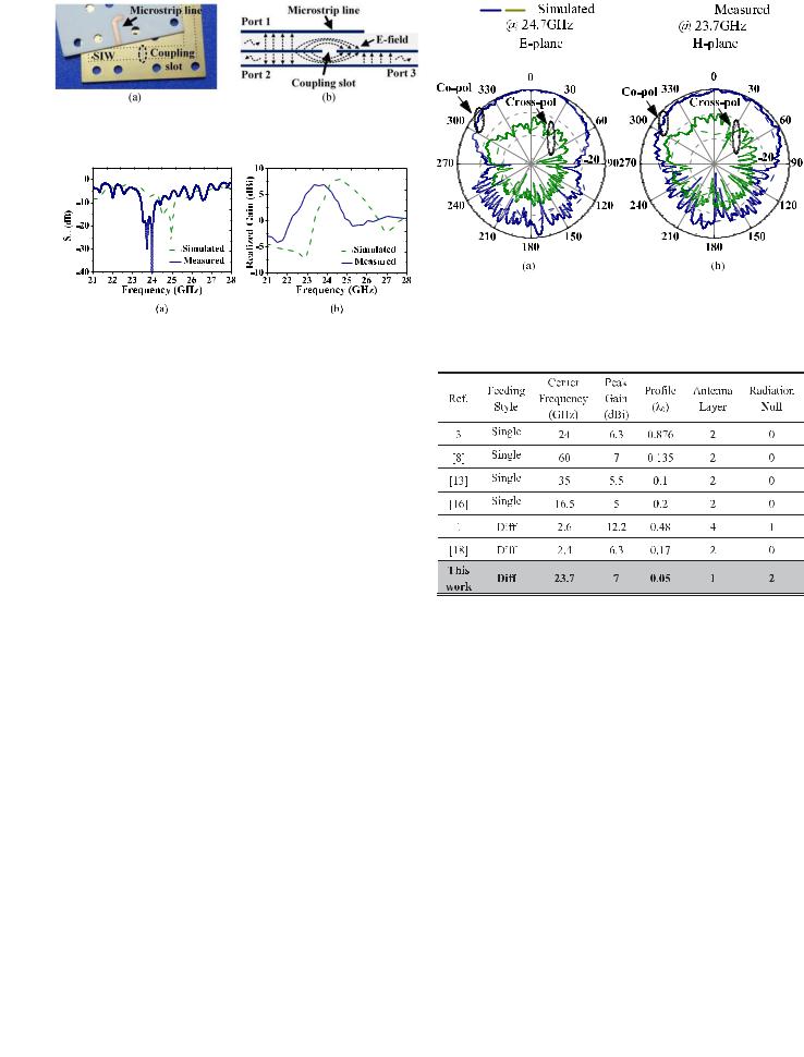
Fig. 10 shows the simulated and measured reflection coefficients and boresight realized gains of the proposed antenna integrated with the balun network. The measured results have a slight frequency shifting of about 4%, which is caused by fabrication tolerance. In Fig. 10(a), the achieved −10 dB impedance bandwidth is 3.16%, slightly smaller than the simulated one (3.23%). Fig. 10(b) shows the gain response of the antenna prototype. The insertion loss of the balun and transmission loss of the differential network are used to calibrate the simulated and measured realized gains, respectively. The measured peak realized gain is 7 dBi, which is lower than the simulated realized gain (8 dBi). Two measured radiation nulls at 21.6 and 25.2 GHz are generated at both the lower and upper band edges showing a tendency similar to the simulated results.
Fig. 11 shows the simulated and measured radiation patterns of the antenna integrated with the balun network. Generally, symmetrical radiation patterns are achieved in both E- and H- planes. The measured 3 dB beamwidths in the E-plane and H-plane are 72° and 58°, respectively. The isolation between coand cross polarization is larger than 20 dB in the E-plane and 18 dB in the H-plane. The deterioration of cross polarization is caused by the phase and magnitude imbalance of the balun and the overall asymmetry structure.
The comparisons between the proposed DRA and previously reported works are summarized and listed in Table I, which focus on the operating frequency, gain, profile, number of antenna layers, and radiation nulls. Compared with the reported DRAs, it can be found that the proposed differential antenna shows a single-layer structure, lower profile, higher boresight gain, and
better frequency selectivity. Although the reported differentially fed antenna in [1] has a high boresight gain, it shows a profile of about 0.48λ0 and was manufactured in four layers. The low profile of the proposed antenna benefits from the coplanar feeding method. Meanwhile, the antenna achieves filtering function with two radiation nulls. The combination performance of the proposed DRA is outstanding for mm-Wave applications.
IV. CONCLUSION
In this letter, a differentially coplanar-fed method for a lowprofile mm-Wave DRA has been proposed. A filtering function has also been realized, and two radiation nulls have been induced at both upper and lower band edges. The proposed DRA was fabricated with a single-layer laminate by using standard PCB technology that minimized the errors in the assembly procedure. With differential feeding, the proposed antenna shows low cross polarization and symmetric radiation patterns and is able to be directly integrated in differential systems. The method presented in this letter is applicable to designing a DRA for reducing profile and realizing filtering performance, and has been verified by a prototype integrated with a balun network.
790 |
IEEE ANTENNAS AND WIRELESS PROPAGATION LETTERS, VOL. 18, NO. 4, APRIL 2019 |
REFERENCES
[1]R. D. Gupta and M. S. Parihar, “Differentially fed wideband rectangular DRA with high gain using short horn,” IEEE Antennas Wireless Propag. Lett., vol. 16, pp. 1804–1807, 2017.
[2]H. Tang, C. W. Tong, and J. X. Chen, “Differential dual-polarized filtering dielectric resonator antenna,” IEEE Trans. Antennas Propag., vol. 66, no. 8, pp. 4298–4302, Aug. 2018.
[3]Y. M. Pan, K. W. Leung, and K. M. Luk, “Design of the millimeter-wave rectangular dielectric resonator antenna using a higher-order mode,” IEEE Trans. Antennas Propag., vol. 59, no. 8, pp. 2780–2788, Aug. 2011.
[4]R. K. Mongia, A. Ittibipoon, and M. Cuhaci, “Low profile dielectric resonator antennas using a very high permittivity material,” Electron. Lett., vol. 30, no. 17, pp. 1362–1363, Aug. 1994.
[5]K. P. Esselle, “A low-profile rectangular dielectric-resonator antenna,” IEEE Trans. Antennas Propag., vol. 44, no. 9, pp. 1296–1297, Sep. 1996.
[6]K. W. Leung, K. M. Chow, and K. M. Luk, “Low-profile high-permittivity dielectric resonator antenna excited by a disk-loaded coaxial aperture,”
IEEE Antennas Wireless Propag. Lett., vol. 2, pp. 212–214, 2003.
[7]L. Lu, Y. C. Jiao, W. Liang, and H. Zhang, “A novel low-profile dual circularly polarized dielectric resonator antenna,” IEEE Trans. Antennas Propag., vol. 64, no. 9, pp. 4078–4083, Sep. 2016.
[8]M. O. Sallam et al., “Micromachined on-chip dielectric resonator antenna operating at 60 GHz,” IEEE Trans. Antennas Propag., vol. 63, no. 8, pp. 3410–3416, Aug. 2015.
[9]Y. M. Pan and S. Y. Zheng, “A low-profile stacked dielectric resonator antenna with high-gain and wide bandwidth,” IEEE Antennas Wireless Propag. Lett., vol. 15, pp. 68–71, 2016.
[10]X. Y. Dong, W. W. Yang, H. Tang, and J. X. Chen, “Wideband lowprofile dielectric resonator antenna with a lattice structure,” Electron. Lett., vol. 53, no. 19, pp. 1289–1290, 2017.
[11]M. Abedian, H. Oraizi, S. K. Abdul Rahim, S. Danesh, M. R. Ramli, and M. H. Jamaluddin, “Wideband rectangular dielectric resonator antenna for low-profile applications,” Microw., Antennas Propag., vol. 12, no. 1, pp. 115–119, Jan. 2018.
[12]Nasimuddin and K. P. Esselle, “A low-profile compact microwave antenna with high gain and wide bandwidth,” IEEE Trans. Antennas Propag., vol. 55, no. 6, pp. 1880–1883, Jun. 2007.
[13]K. Gong and X. H. Hu, “Low-profile substrate integrated dielectric resonator antenna implemented with PCB process,” IEEE Antennas Wireless Propag. Lett., vol. 13, pp. 1023–1026, 2014.
[14]H. Chu and Y. X. Guo, “A novel approach for millimeter-wave dielectric resonator antenna array designs by using the substrate integrated technology,” IEEE Trans. Antennas Propag., vol. 65, no. 2, pp. 909–914, Feb. 2017.
[15]J. Y. Jin, S. Liao, and Q. Xue, “Design of filtering-radiating patch antennas with tunable radiation nulls for high selectivity,” IEEE Trans. Antennas Propag., vol. 66, no. 4, pp. 2125–2130, Apr. 2018.
[16]A. Rashidian, L. Shafai, M. Sobocinski, J. Perantie,¨ J. Juuti, and H. Jantunen, “Printable planar dielectric antennas,” IEEE Trans. Antennas Propag., vol. 64, no. 2, pp. 403–413, Feb. 2016.
[17]K. M. Luk and K. W. Leung, Dielectric Resonator Antennas. London, U.K.: Research Studies Press, 2003.
[18]X. S. Fang, K. W. Leung, E. H. Lim, and R. S. Chen, “Compact differential rectangular dielectric resonator antenna,” IEEE Antennas Wireless Propag. Lett., vol. 9, pp. 662–665, 2010.