

диафрагмированные волноводные фильтры / 6d5ec612-bf51-4838-919e-e7af139bbeff
.pdfIEEE Africon 2017 Proceedings
An Efficient Design Workflow of a
Compact Ridged Waveguide Filter
Theunis S. Beukman
CST – Computer Simulation Technology AG
64289 Darmstadt, Germany
Email: Theunis.BEUKMAN@3ds.com
Abstract—This paper describes an efficient design workflow of a dual-mode bandpass filter. The device consists of square ridge resonators that are coupled through broadside irises in the waveguide. This allows for a compact solution where full control over the individual couplings is possible. A new tuning process is proposed which involves the extraction of a coupling matrix for the detuned 3D filter. The final result shows an equiripple passband with 1% FBW and four transmission zeros in the stopband which provide high selectivity.
Keywords—Multimode filters, EM simulation, filter tuning
I. INTRODUCTION
the EM structure inherently sensitive and therefore becomes increasingly difficult to tune it up to a suitable state. In this paper a different approach is proposed which involves the direct extraction of a coupling matrix for the detuned response.
The design workflow is demonstrated with a dual-mode filter consisting of an unconventional cavity configuration, where square ridge resonators [5] are coupled through broadside irises (see Fig. 1). This not only provides good control over the individual coupling coefficients, but it also produces a compact solution for satellite communication systems.
Modern communication systems are becoming increasingly demanding on the utilization of the frequency spectrum. In order to realize some of these stringent specifications channel filters are required. Satellite systems in particular have many requirements for such filter designs. Size and weight is typically very restricted in a payload and needs to be taken into account, while the filter response should produce steep cut-off to avoid channel interference and adhere to different standards.
Cavity filters are typically the preferred choice due to its power handling capabilities, though the downside is that they are bulky and heavy. This is where multi-mode cavity filters become very attractive. They utilize a number of modes in a single cavity and therefore significantly reduces the overall size [1]. In addition they also provide the possibility of crosscouplings where single mode resonators may fail due to physical restrictions.
There are several simulation techniques that could be used in the tuning process of coupled-resonator filters [2]. A common approach is to sequentially build up the filter by adding only one resonator at a time, while the group delay of the reflected signal is used as the figure of merit for the optimization [3]. Another approach is to apply the inverse chirp Z-transformation to the reflected signal and from the transient response identify the individual detuned resonators and couplings [2]. One could also add additional ports to the full-wave simulation model and connect lumped components in a coupled schematic for space mapping [4]. All of these techniques typically involve using an equivalent circuit as a surrogate model where intermediate results can quickly be obtained as a reference during the process.
Applying these techniques to a multi-mode cavity filter can however be cumbersome and even impossible in many cases. Furthermore, the required narrow bandwidth makes
Fig. 1. The 8th order ridged waveguide filter model.
II. FILTER RESPONSE AND TOPOLOGY
The filter specifications are chosen for satellite communication, where selectivity of the channel and compactness of the device are the two highest priorities. The filter topology is obtained using the synthesis software tool CST R Filter Designer 3D and the response is shown in Fig. 2(a). The centre frequency (f0) is at 10 GHz with a passband return loss of more than 20 dB over a 100 MHz bandwidth, which is equal to 1% in fractional bandwidth (FBW). To ensure high selectivity an 8th order transfer function is used with two symmetric pairs of transmission zeros around the passband.
There are a number of possible canonical coupling matrices that would produce such a response. A convenient layout is
569
978-1-5386-2775-4/17/$31.00 ©2017 IEEE

IEEE Africon 2017 Proceedings
(a)
(b)
Fig. 2. (a) The S-parameter response of (b) the synthesized coupling matrix, with the filter topology shown in the inset.
chosen that consists of two cascaded quadruplet sections which are directly responsible for the two transmission zero pairs. The corresponding coupling matrix is given in Fig. 2(b) along with the illustrated filter topology – where the circles represent the resonators (or resonant modes) and the squares represent the source/load with all the appropriate coupling connections.
III. RESONATOR OPERATION AND DESIGN
The resonator chosen to ensure a compact physical solution is a ridged waveguide dual-mode resonator that was first introduced by Bastioli [5]. The resonator consists of a rectangular waveguide with a large square ridge inside as shown in Fig. 3. Two orthogonal quasi-TEM modes can exist in the narrow gap between the ridge and the top wall – approximating a parallel plate. Note that the arrows in Fig. 3 indicate the direction of the current flow of each mode on the ridge. As a consequence the gap along with the ridge size directly determines the resonant frequencies of these modes, as well as the stopband separating the next higher-order mode. The resonator is implemented in WR-90 waveguide technology which is best suited for the operation at 10 GHz.
When such a ridge is positioned at the transversal centre of a straight waveguide (refer to Fig. 4), the fundamental T E10 mode will only excite the longitudinal-directed mode. The orthogonal mode possesses odd symmetry in the transversal direction and therefore is unaffected by the waveguide mode. The principle is illustrated in Fig. 4, where the waveguide mode propagating from the source couples into the longitudinal ridge mode ("mode1") and out again into the load. However, since the ridge symmetry is perturbed by the one chamfered corner, the longitudinal mode also couples into the transversal mode ("mode2"). This leads to a type of branchline filter topology which produces a dual-band filter response with a transmission zero at the centre frequency.
Fig. 4. A single ridged resonator placed in a rectangular waveguide excited with the fundamental T E10 mode and its response.
IV. MODAL COUPLING MECHANISMS
The coupling between ridges as well as a ridge to source/load can be controlled through simple H-plane irises. In [5] this is demonstrated with a 4th order quadruplet filter topology as shown in Fig. 5. Here the cross-coupling between modes 1 and 4 is controlled through the higher-order evanescent T E20 mode in the iris (depicted by the orange box). The width of this iris mostly controls the coupling between the transversal modes (defined w.r.t. the input/output propagation direction), while the length of the iris mostly controls the coupling between the longitudinal modes.
Fig. 3. Ridged waveguide resonator with dimensions and modal current directions. For resonance at 10 GHz in the WR-90 waveguide the ridge length is 12.76 mm while the gap is 1.5 mm.
Fig. 5. A conventional quadruplet configuration employing H-plane iris couplings along with its S-parameter response.
Using this configuration for the 8th order filter – by simply cascading the resonators with H-plane irises – will result in a bulky device. More importantly, these irises sustain coupling between both modal pairs and thus unwanted coupling will be unavoidable between modes 3 and 6 in the filter topology
570

IEEE Africon 2017 Proceedings
of Fig. 2. It is thus more attractive having distinct coupling mechanisms for each individual coupling coefficient.
Therefore in this paper a different approach is followed – instead of coupling between resonators in the H-plane, the resonators are stacked on top of each other as illustrated in Fig. 6. The couplings can then be established through irises in the broadside walls, thus allowing the aligned modes in adjacent resonators to be coupled through separate E-plane irises. This leads to an overall compact geometry.
other dimensions of the iris are established to minimize the unwanted coupling, without compromising the range of the desired CBW.
The electric coupling shown in Fig. 7(b) produces the values for coefficients m14 and m58, respectively. The distinction of this type of coupling to the magnetic coupling is that it has a lower odd-mode resonant frequency than that of the even-mode. This is accomplished by a thin (1 mm) but wide capacitive iris. As seen from the graph the CBW is controlled by the offset of the iris to the resonator wall.
Finally the other magnetic coupling for coefficient m45 is obtained by a similar iris as in Fig. 7(a), but with a shorter length since the ridge gaps are on opposite sides. This can be seen from the cross-sectional views of the complete model in Fig. 8, where all the broadside irises are indicated along with its corresponding coupling coefficients. Note that the source and load simply couple in through H-plane irises (see Fig. 6).
Fig. 6. The proposed ridged resonator configuration with an illustration of all the different coupling mechanisms.
The first magnetic coupling, serving coefficients m23 and m67, is established between the aligned modes where the ridge gaps face each other as shown in Fig. 7(a). Here the evenand odd-mode current distributions are shown for this coupling system, where a magnetic wall is placed on the symmetry axis of the current distribution to ensure the calculation of only the appropriate eigenmodes [6]. From the graph it is clear that the coupling bandwidth (CBW) can be controlled by the height of the iris.
(a) |
(b) |
Fig. 7. The eigenmode current distributions of the (a) magnetic and (b) electric couplings established through the broadside irises. Note that only the currents on ridges are depicted. Each graph shows the dependency of the CBW on a corresponding geometrical parameter.
In a separate calculation the magnetic wall is replaced by an electric wall and used to determine the unwanted coupling between the orthogonal ridge modes. With this information the
Fig. 8. Cross-sectional views of the complete structure in planes A-A and B-B, where the different broadside iris couplings are indicated.
To establish the orthogonal mode couplings within the cavities (i.e. m12, m34, m56 and m78), a single corner of each ridge is chamfered. These chamfers need to be carefully positioned within the complete layout, in order to avoid phase cancellation which will negate the designed iris couplings. Thus to avoid this all the chamfers are orientated in the same direction. Furthermore, they are also placed on opposite sides to the coupling irises of coefficients m23, m14, m67 and m58 (refer to Fig. 1) in order to have minimal affect on the broadside couplings.
Finally, with all of these coupling mechanisms brought together, the complete filter model is solved using a Model Order Reduction (MOR) technique based on the Finite Element Method (FEM) [6]. The S-parameter results are given in Fig. 9 where it is clear that the filter is completely detuned. This is expected from the loading effects of the different components.
571

IEEE Africon 2017 Proceedings
Fig. 10. The extracted coupling matrix for the results in Fig. 9, where the percentages indicate how far the coefficients are from that of the synthesized comparison matrix. The inductor symbols indicate parasitic coupling coefficients.
Fig. 9. The S-parameters of the initial detuned 3D filter.
V. TUNING OF THE COMPLETE 3D STRUCTURE
The coupling matrix of this detuned model is extracted with the synthesis software tool CST R Filter Designer 3D and the results shown in Fig. 10. To achieve this the software applies a polynomial fitting to the detuned S-parameters and then generates a new coupling matrix based on the polynomials. However, due to parasitic couplings – for example in this case between mode 1 and 3 – the synthesized matrix is no longer a valid comparison. Thus a so-called ’synthesized comparison matrix’ is generated which maintains the equiripple passband with the parasitic couplings included. This is used therefore as a comparison for the extracted matrix, where the deviations are indicated by percentage values for each coefficient as shown in Fig. 10.
Asymmetry is observed in the transmission zero pairs of the detuned response (Fig. 9) and is an indication of coupling between unintended modes. To include this effect the software places the parasitic couplings within each quadruplet section of the intended filter topology. The corresponding matrix entries are indicated by the inductor symbols in Fig. 10 and their values equalized within each quadruplet – i.e. m13 = m24 and m57 = m68. Additional transmission zeros (also in the complex plane) can be compensated for by adding more parasitics to the matrix; however, in this case they are located far enough from the passband and can therefore be neglected.
The next step is to determine what the new dimensions should be to compensate for the unwanted deviations found in the extracted coupling matrix. For this the eigenmode results
are used where the relation between the filter parameters (f0, external Q-factor and CBW) and the appropriate geometrical parameters are obtained – as outlined in the previous section. As seen from Fig. 10 the diagonal coefficients have some of the largest deviations, which means that the resonant frequencies are out. This is compensated for by changing the corresponding ridge lengths that control these values in the 3D filter geometry.
The updated model is again simulated with the MOR technique and the new S-parameters are shown in Fig. 11, depicted as ’state2’. Clearly this already helped to achieve some matching around the centre frequency. Again the results are used to extract a new coupling matrix and as expected, the deviations of the diagonal coefficients have improved substantially. Next the largest deviations of the CBW’s are tuned in the simulation model.
Fig. 11. The S-parameters of the 3D model in state2 and state8 of the tuning process.
This tuning cycle is followed until an appropriate filter state is reached – in this case where the diagonal coefficient errors in the extracted matrix are below 5% while the majority of the other errors are below 8%. The response is depicted in Fig. 11 as ’state8’, since it took only 8 iterations to tune all 18 geometrical parameters in the 3D model up till this point.
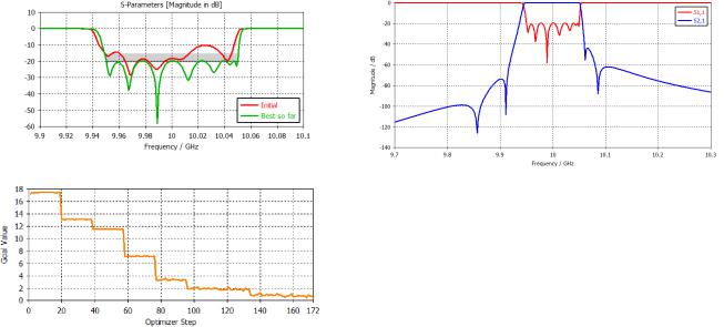
With the model’s response close to its desired specifications a direct optimization is applied in the full-wave simulation. This is simply for the fine-tuning of the passband in order to obtain |S11| < -20 dB. The Trust Region Framework algorithm [6] is selected to do a local search over all 18 parameters and the resulting |S11| curves are shown in Fig. 12(a).
572
IEEE Africon 2017 Proceedings
(a)
(b)
Fig. 12. The optimization result of (a) |S11| and (b) the goal function.
It is important to note here that this model is very sensitive due to its narrowband response. Therefore the mesh noise
–which is a common problem in any FEM-based code [7]
–would make it close to impossible to efficiently reach convergence as illustrated by the resulting goal function in Fig. 12(b). To overcome the mesh noise a technique was employed that moves the tetrahedral mesh nodes during each parameter update, instead of re-meshing the entire structure [6].
The final S-parameters of this model are shown in Fig. 13 where an equiripple passband is achieved. Unfortunately the transmission zeros are located asymmetrically around the passband – providing steeper cut-off at the upper side while worsening the cut-off on the lower side. This effect is caused by the parasitic couplings in the structure which are difficult
to fully control. The overall size of the simulation model as shown in Fig. 1 is 23 x 29 x 60 mm3.
Fig. 13. Final S-parameters of the tuned 3D filter.
VI. CONCLUSION
A complete workflow for the design of a ridged waveguide
filter was described. The device employs broadside coupled irises that enables an overall compact filter implementation.
The proposed tuning process is based on a coupling matrix extracted for the detuned device. The design approach proved to be an efficient solution for such a highly sensitive filter with 1% FBW.
REFERENCES
[1]A. E. Atia and A. E. Williams, “New types of waveguide bandpass filters for satellite transponders,” in COMSAT Technical Review, vol. 1, no. 1, 1971.
[2]F. Hirtenfelder, “Tuning methods for bandpass filters using CST STUDIO SUITE solver technology,” in 4th CST European User Group Meeting, 2009.
[3]J. B. Ness, “A unified approach to the design, measurement, and tuning of coupled-resonator filters,” IEEE Transactions on Microwave Theory and Techniques, vol. 46, no. 4, pp. 343–351, Apr 1998.
[4]Q. S. Cheng, J. C. Rautio, J. W. Bandler, and S. Koziel, “Progress in simulator-based tuning – the art of tuning space mapping,” IEEE Microwave Magazine, vol. 11, no. 4, pp. 96–110, Jun 2010.
[5]L. M. S. Bastioli and R. Sorrentino, “A novel class of compact dualmode rectangular waveguide filters using square ridge resonators,” in 38th European Microwave Conference (EuMC), 2008, pp. 626–629.
[6]CST – Computer Simulation Technology AG, Darmstadt, Germany. CST STUDIO SUITE R . [Online]. Available: http://www.cst.com
[7]S. Ratnajeevan, H. Hoole, K. Weeber, and S. Subramaniam, “Fictitious minima of object functions, finite element meshes, and edge elements in electromagnetic device synthesis,” IEEE Transactions on Magnetics, vol. 27, no. 6, pp. 5214–5216, Nov 1991.
573