

диафрагмированные волноводные фильтры / 8c70a300-4011-4997-b1b8-8f81715c73d7
.pdfA Vertical Integration of High-Q Filters with Patch Antennas with Enhanced Bandwidth and High Efficiency
Yazid Yusuf, and Xun Gong
Department of Electrical Engineering and Computer Science, University of Central Florida, Orlando, FL, 32816, U. S. A. Email: yazidn@gmail.com; xungong@mail.ucf.edu.
Abstract — A new approach to integrate high quality(Q)- factor 3-D vertical cavity filters with patch antennas into a single unit is presented in this paper. This integrated filter/antenna system exhibits small footprint, high efficiency, and enhanced bandwidth. The patch antenna is designed to provide an additional transmission pole for the filtering function and work as a highly efficient radiator. In addition, this integrated patch antenna with a filter can achieve a bandwidth much larger than a standalone patch antenna with the same geometry. A prototype three-pole Chebyshev filter/antenna is demonstrated at X band. The center frequency and fractional bandwidth of the filter/antenna system are 10.27 GHz and 8.7%, respectively. Due to the high Q factor (~700) of the cavity resonator and near lossless transition between the antenna and filter, the overall efficiency of the filter/antenna system is simulated to be as high as 91%. The reduced footprint, enhanced bandwidth, and lowloss performance of these integrated filter/antenna systems make them particularly useful for phased array applications. The measured impedance matching, efficiency, gain, and radiation pattern closely agree with simulation results.
Index Terms — Bandpass filter, cavity resonator, packaging, patch antenna.
I. INTRODUCTION
Patch antennas have been widely used in various communications and radar systems due to the ease of fabrication, low profile, and the flexibility of design in terms of polarization, and radiation pattern etc. Particularly they are very popular in phased array antenna systems since patch antenna arrays are thin, broad-side radiating, and easy to achieve beam steering capability with the help from phase shifters.
However, patch antennas are usually narrowband due to their high-Q resonant nature. Bandwidth enhancement can be achieved by utilizing thick substrates with low dielectric constants, parasitic resonant patches [1], or resonant slots within the patch antenna [2]. The increased bandwidth using these approaches is usually at the expense of losing efficiency.
High Q-factor filters are necessary to improve the signal-to- noise ratio and consequently reduce the noise figure of the receiver for communications or radar systems. Due to the limitation of size, weight, and Power (SWaP) requirements inside practical systems, having high-Q filters and highly efficient wide-band patch antennas becomes very difficult, if not impossible.
Fig. 1. Exploded view of a vertically integrated three-pole filter/antenna with two cavity resonators and one patch antenna.
The traditional way to incorporate high-Q filters and antennas into a system is using standard 50-ohm ports such as coaxial connectors or transmissions lines. The separate design of filters and antennas individually often renders large size or detuned filter responses [3]. As shown in [4], a microstrip patch antenna was integrated with a coplanar waveguide (CPW) resonator filter. In this design, the patch antenna acted as both a radiator and an additional resonator for the filter. Therefore, higher out-of-band rejection was achieved with less number of resonators inside the filter. However, the planar structure used in [4] was very limited in Q factor performance, i.e. < 200. Furthermore, the radiation from the transmission line resonators could significantly degrade the out-of-band performance [5].
A new way to realize integrated high-Q filters with highlyefficient patch antenna is presented in this paper and illustrated in Fig. 1. The entire system consists of two high Q- factor cavity resonators and one resonant patch antenna. They are vertically stacked to greatly reduce the footprint. A thirdorder Chebyshev filtering function is realized. In addition, the bandwidth of the entire filter/antenna far exceeds that of a standalone patch antenna. Efficiencies as high as 91% have been achieved in simulations. A prototype of the designed filter/antenna system is fabricated and very good agreement between measured and simulated results is observed.
978-1-61284-757-3/11/$26.00 C2011 IEEE
Lr1
Ws
Pc
W |
|
Ls |
|
Xs
(a) |
(b) |
Lp
d
Wp
(c) |
(d) |
Fig. 2. Schematics of (a) SMA coaxial feeding and coupling slot;
(b) coupling slot and via; (c) coupling via and patch antenna; and
(d) vertical stack. (W = 12.9; Pc = 2.7; Ls = 5.7; Ws = 0.5; Xs = 0.9;
Lr1 = 15.7; Lr2 =16; Pp = 3.1; c = 6.5; d = 2.3; Lp = 9.1; Wp = 14; h1 = 1.6; h2 = 0.8) Dimensions are in mm.
II. FILTER/ANTENNA SYNTHESIS
As shown in Fig. 1, three substrate layers are used to form the integrated filter/antenna structure. The dielectric material used here is Rogers Duroid/RT 5880 (εr = 2.2 and tanδ = 0.0009). The cavity resonators are realized using closelyspaced metallic vias, the spacing between which is very small compared with the wavelength of operation. The internal coupling between the two cavity resonators is through a slot in the common ground plane between the two. The coupling between the resonator and patch antenna is through a coupling via connecting them together. The external coupling to the cavity resonator is achieved by using a short-ended SMA coaxial connector. As mentioned earlier, this integrated filter/antenna exhibits three transmission poles, similar to a three-pole filter. Therefore, a rigorous synthesis procedure must be followed to ensure that the integrated filter/antenna has all the analogues of an equivalent three-pole filter in terms of resonators, internal couplings, and external couplings. The schematics of the integrated filter/antenna from different view angles are shown in Fig. 2.
A reference three-pole Chebyshev filter with 8% fractional bandwidth at 10.16 GHz was synthesized. The design parameters of this filter are:
k12 = k23 = 0.054 |
(1) |
Qext,1 = Qext,2 = 17.2 |
(2) |
If this three-pole filter were realized using the vertical stacking as shown in Fig. 1, it would be symmetric with respect to a horizontal plane in the middle of ground planes 2 and 3. In this integrated filter/antenna design, the patch antenna replaces the top cavity resonator. The k23 now
1  : n 1
: n 1
(a) |
(b) |
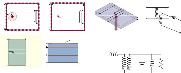
Fig. 3. (a) Schematic of a waveguide excited by a coaxial probe and
(b) its equivalent circuit.
Fig. 4. The equivalent circuit of a probe-fed patch antenna.
becomes the coupling between the middle cavity and patch antenna which is achieved through a coupling via. The radiation Q factor (Qrad) of the patch antenna is equivalent to
Qext,2 of the reference filter. The rest of this section will describe the details on how to synthesize these design
parameters for the integrated filter/antenna in order to realize the same filtering functions of the reference filter. It will also be shown in Section III that the integrated patch antenna exhibits the same radiating characteristics as a standalone patch antenna but with a much wider frequency range of operation. This bandwidth enhancement can be explained by viewing the two cavity resonators preceding the patch antenna as a multisection impedance transformer that matches the patch to the input port over a larger frequency range.
A. Modeling the Coupling Via Inside a Waveguide
In order to build the equivalent circuit for the coupling via, we first studied a waveguide which is fed by a coaxial probe as shown in Fig. 3(a). This coaxial probe has the same crosssectional dimensions as the coupling via. The inner and outer diameters of the coaxial probe are 0.635 and 1.27 mm, respectively. This structure was investigated by Harrington for thin feeding vias [6]. Its equivalent circuit is shown in Fig. 3(b). This equivalent circuit uses an ideal transformer with 1:n1 turn ratio and a reactance of X1 from the probe. Using a stationary treatment and selecting the wave impedance Zow as the characteristic impedance of the waveguide, the turn ratio n1 is given by [6]:
2 |
= |
2h tan( kh ) |
2 |
2 |
( |
πc |
) |
(3) |
||
n1 |
|
kh |
|
sin |
|
W |
||||
|
|
W |
|
|
|
|
|
|
||
where h and W are the waveguide height and width, respectively; c is the distance between the center of the probe and the sidewall of the waveguide; k is the wave number in the
978-1-61284-757-3/11/$26.00 C2011 IEEE

dielectrically-loaded waveguide.
B. Modeling a Probe-Fed Patch Antenna
The probe-fed patch antenna is modeled using an equivalent circuit shown in Fig. 4. The reactance X2 represents the probe inductance. The position of the probe d from the edge of the patch determines the turn ratio n2 which can be calculated using:
n2 |
= cos( |
πd |
) |
(4) |
|
||||
|
|
L p |
|
|
The probe position d is used to change the impedance level of the patch. The impedance level is maximum (minimum) when the probe is at the edge (center).
Qrad is primarily controlled by the dielectric constant and the thickness of the substrate [7]. Lower Qrad can be obtained using thicker substrates and lower dielectric constants.
C.Filter/Antenna Modeling
With the equivalent circuits presented in the previous two subsections, the equivalent circuit of the entire filter/antenna system can be constructed as shown in Fig. 5. K inverters are used to represent the external coupling from the SMA connector to the bottom resonator and the inter-resonator coupling between the two cavity resonators. The turn ratio n1 and n2 are controlled by the probe position c and d, respectively, as illustrated in Fig. 2. The collective effects from the two parameters determine the impedance level of the patch as seen by the middle cavity resonator. The impedance resulting from the shorted-ended waveguide with the length Pp is equal to jXp which is given by:
jX p = jZow tan(βPp ) |
(5) |
where β is the propagation constant of the waveguide. By reflecting the patch impedance through the two transformers, the simplified equivalent circuit is shown in Fig. 6. The equivalent circuit element values are:
|
|
|
|
|
n |
|
|
|
2 |
|
|
|
|
|
n |
2 |
|
2 |
|
|
|||||
|
R |
|
' = |
|
|
|
2 |
|
|
|
R |
|
, |
L |
|
' = |
|
|
L |
|
(6) |
||||
|
|
|
|
|
|
|
|
|
|
|
|
||||||||||||||
|
|
|
n |
|
|
|
|
|
|
||||||||||||||||
|
|
|
p |
|
|
|
|
|
|
|
p |
|
p |
n |
1 |
|
|
p |
|||||||
|
|
|
|
|
|
1 |
|
|
|
|
|
|
|
|
|
|
|
|
|
||||||
|
|
|
|
|
n |
|
|
2 |
|
|
|
|
|
|
|
j( X 1 + X 2 ) |
|
||||||||
C |
p |
' = |
1 |
|
|
|
C |
p |
, |
jX |
s |
= |
(7) |
||||||||||||
|
|
|
|
|
|||||||||||||||||||||
|
|
|
|
|
|
|
|
|
|
|
|
|
|
|
|
|
|
2 |
|
||||||
|
|
|
|
n2 |
|
|
|
|
|
|
|
|
|
|
|
|
|
|
n1 |
|
|
||||
For the convenience of further analysis, the two cavity resonators are modeled by series LC circuits in Fig. 6. In order to see the effect of the equivalent circuit parameters and their role in determining the coupling between the middle cavity resonator and patch antenna, the equivalent circuit in Fig. 7 is used. Using a coupling of modes formulation [8], the coupling coefficient k23 between the middle cavity resonator and patch antenna is approximately given by:
k23 |
= |
1 |
|
X p |
1 |
(8) |
|
2πfo |
|
X p + X s |
|
L2C p ' |
|||
|
|
|
|
|
|||
Equation (8) shows that this coupling can be controlled by changing Pp. The coupling also depends on the reflected patch capacitance Cp’, which can be controlled by the proper
Fig. 5. Equivalent circuit of the filter/antenna system. 
Fig. 6. Simplified equivalent circuit of the filter/antenna system.
Fig. 7. Equivalent circuit of the patch antenna coupled to the middle cavity resonator.
selection of n1 and n2 as shown in equation (7). The impedances jXs and jXp in the coupling network between the middle cavity resonator and patch antenna detune their resonant frequencies. However, this frequency detuning effect can be conveniently accounted for with the aid of the equivalent circuit in Fig. 5.
Using the developed equivalent circuits and the described design guidelines, a filter/antenna system is designed and simulated using Ansoft High Frequency Structure Simulator (HFSS). The simulated center frequency and bandwidth are 10.16 GHz and 8.0%, respectively. In addition, the filter/antenna responses exactly match the reference filter responses using circuit simulator. The dimensions of the filter/antenna are listed in Fig. 2.
III. FABRICATION AND MEASUREMENT RESULTS
A prototype filter/antenna is fabricated and measured to verify the synthesis procedure described in Section II. Each layer of the entire system is individually fabricated using standard PCB fabrication processes. Then the coupling via is soldered into the patch antenna and middle cavity resonator. An SMA connector is soldered to the bottom resonator to form the feeding port. Finally, all three layers are bonded together using a solder paste inside a reflow oven. Photos of the fabricated filter/antenna are shown in Fig. 8.
The measured filter/antenna S11 agrees very well with simulation results as shown in Fig. 9. The measured center frequency is 10.27 GHz, compared with 10.16 GHz in the simulation. This 1.1% frequency shift is due to the fabrication tolerances. Return losses higher than 12 dB are measured across the filter/antenna passband. It is clearly seen in Fig. 9
978-1-61284-757-3/11/$26.00 C2011 IEEE

that three transmission poles have been achieved with two resonators and one patch antenna. To verify the filtering function of this integrated system, the gain of the filter/antenna system is measured in an anechoic chamber. The measured gain versus frequency is plotted against the simulation results as shown in Fig. 9. Both simulation and measurement results demonstrate the third-order filtering function across a wide frequency range. The measured filter/antenna bandwidth of 8.7% is slightly larger than the simulated 8.0%.
The radiation patterns of the filter/antenna are measured in both E and H-planes. As shown in Fig. 10, the measured patterns match the simulation results at the center frequency. As expected, these radiation patterns are typical for patch antennas. It should be noted that the measured radiation patterns are slightly narrower than in simulation particularly in the E-plane, which corresponds to a higher directivity. Similar radiation patterns are observed across the entire passband. Therefore, the integrated patch antenna is able to function within an 8.7% fraction bandwidth, which is much larger than the bandwidth (approximately 1%) of a probe-fed standalone patch antenna with the same dimensions.
The simulated directivity and gain using HFSS are found to be 8.9 and 8.5 dBi, respectively. Therefore, the overall efficiency of the integrated filter/antenna system is calculated using Gain/Directivity and found to be 91%. The gain at the center frequency is measured to be 8.8 dBi, which is slightly higher than the simulated gain. This is attributed to the slightly larger directivity observed in measurements.
IV. Conclusion
A synthesis approach to seamlessly integrate N high-Q resonators with a resonant patch antenna to realize (N+1)th- order filtering was presented and verified through simulation, fabrication, and measurement. The integrated filter/antenna has small footprints, is highly efficient, and achieves enhanced bandwidth without compromising the high efficiency. This new filter/antenna architecture can enable compact and low-loss RF front ends and phased array systems.
ACKNOWLEDGEMENT
Fig. 8. Photos of the fabricated filter/antenna system.
|
10 |
|
|
|
10 |
|
|
0 |
|
|
|
0 |
|
(dB) |
-10 |
|
|
|
-10 |
|
S-Parameters |
-20 |
|
|
|
-20 |
Gain (dBi) |
-30 |
|
|
|
-30 |
||
|
|
|
|
|
||
|
-40 |
|
Simulated |
|
-40 |
|
|
|
|
Measured |
|
|
|
|
-50 |
|
|
|
-50 |
|
|
8 |
9 |
10 |
11 |
12 |
|
Frequency (GHz)
Fig. 9. Simulated and measured responses of the three-pole vertically integrated filter with a patch antenna.
0 |
0 |
|
0 |
|
|
0 |
330 |
30 |
|
330 |
30 |
||
-5 |
|
|
||||
|
|
-5 |
|
|
|
|
-10 |
|
|
|
|
|
|
|
|
|
|
|
|
|
-15 |
300 |
60 |
-10 |
300 |
|
60 |
-20 |
|
|
||||
|
|
-15 |
|
|
|
|
-25 |
|
|
|
|
|
|
-30 |
|
|
-20 |
|
|
|
-35 |
|
|
|
|
|
|
|
|
|
|
|
|
|
-40 |
270 |
90 |
-25 |
270 |
|
90 |
-35 |
|
|
-20 |
|
|
|
-30 |
|
|
|
|
|
|
|
|
|
|
|
|
|
-25 |
|
|
-15 |
|
|
|
-20 |
240 |
120 |
-10 |
240 |
|
120 |
-15 |
|
|||||
|
|
|
|
|
||
-10 |
|
|
-5 |
|
|
|
-5 |
Simulated |
|
|
Simulated |
|
|
150 |
|
|
150 |
|||
0 |
210 |
0 |
|
210 |
||
Measured |
|
|
Measured |
180 |
||
|
180 |
|
|
|
|
|
|
(a) |
|
|
|
|
(b) |
Fig. 10. Simulated and measured radiation patterns in (a) H-plane and
(b) E-plane at the center frequency.
The authors wish to acknowledge the support of NSF Faculty Early CAREER Award (Grant No. 0846672).
REFERENCES
[1]S. Egashira, and E. Nishiyama, “Stacked microstrip antenna with wide bandwidth and high gain,” IEEE Trans. Antennas Propag., vol. 44, pp. 1533–1534, Nov. 1996.
[2]K. F. Tong, K. M. Luk, K. F. Lee, and R. Q. Lee, “A broad-band U-slot rectangular patch antenna on a microwave substrate,” IEEE Trans. Antenna Propag., vol. 48, pp. 954–960, June 2000.
[3]J. H. Lee, N. Kidera, G. Dejean, S. Pinel, J. Laskar, and M. M. Tentzeris, “A V-band front-end with 3-D integrated cavity filters/duplexers and antenna in LTCC technologies,” IEEE
Trans. Microw. Theory Tech., vol. 54, no. 7, pp. 2925-2936, July 2006.
[4]A. Abbaspour-Tamijani, J. Rizk, and G. Rebeiz, “Integration of filters and microstrip antennas,” 2002 IEEE AP-S Digest, pp. 874-877, June 2002.
[5]C. Lin, and S. Chung, "A compact edge-fed filtering microstrip antenna with 0.2 dB equal-ripple response," Proc. 39th EuMC, Rome, Italy, pp. 378-380, Sept. 2009.
[6]R. F. Harrington, Time-harmonic electromagnetic fields, Wiley, 2001.
[7]C. A. Balanis, Antenna theory: Analysis and design, Wiley, 2005.
[8]H. A. Haus, Waves and fields in optoelectronics, Prentice-Hall, Englewood Cliffs, 1984, ch. 7.
978-1-61284-757-3/11/$26.00 C2011 IEEE