

диафрагмированные волноводные фильтры / 56c80adb-0454-463f-ab49-ea27e66b27ac
.pdfThis article has been accepted for publication in a future issue of this journal, but has not been fully edited. Content may change prior to final publication. Citation information: DOI 10.1109/TAP.2019.2938574, IEEE Transactions on Antennas and Propagation
SUBMITTED TO THE IEEE TRANSACTIONS ON ANTENNAS AND PROPAGATION |
1 |
Design of Compact, Single-Layered Substrate Integrated Waveguide
Filtenna with Parasitic Patch
Kun-Zhi Hu, Ming-Chun Tang, Senior Member, IEEE, Dajiang Li, Yang Wang, and Mei Li, Member,
IEEE
Abstract— A compact, single-layered substrate integrated waveguide (SIW) filtenna with parasitic patch is synthesized and designed. A half-mode substrate-integrated rectangular cavity (HMSIRC) is adopted as the first stage resonator to reduce the circuit size. A parasitic patch functioning as the last stage resonator as well as the radiator is arranged closely to the HMSIRC so as to enhance the operational bandwidth and facilitate the filtering performance. Two broadside radiation nulls are realized at both the upper and lower band-edges to sharpen the band-edge roll-off rate: One is generated by the interaction between the HMSIRC and the parasitic patch, and the other is introduced by placing two pairs of shorting posts under the parasitic patch. The standard filter synthesis technology is utilized to guide the filtenna design. The optimized prototype was fabricated and measured. The measured results, in good agreement with simulated values, indicated the proposed filtenna provides a 5.1% fractional bandwidth, a maximum realized gain of 6.3 dBi, and a flat passband gain response along with excellent out-of-band selectivity, even with ultra-low profile 0.015λ0 and small volume 0.005λ03.
Index Terms—Single-layered antenna, filtenna, parasitic patch, radiation null, substrate integrated waveguide (SIW)
I. INTRODUCTION
With the rapid development of modern wireless communication systems, the physical space of RF front-ends constructed by various kinds of microwave and millimeter-wave components are increasingly limited. The miniaturization and integration of these components have attracted tremendous research interest in recent years.
The emerging substrate integrated waveguide (SIW) is considered as a promising candidate for high-density integrated circuits due to its advantages of low loss, low cost, high quality factor and easy integration with other planar circuits [1], [2]. Numerous researches on filter and antenna designs by usage of SIW technology are widely investigated [3]-[5]. In most RF front-end circuits, the filter is cascaded right after the antenna for spurious signal suppression. Conventionally, these two elements are design separately and connected by standard 50-Ωtransitions, which would not only degrade system performance but also increase the circuit area because of the
Manuscript received on 18 Jan., 2019; revised on 24 Jun., 2019; and accepted on 08 Aug., 2019. This work was supported in part by the Graduate Scientific Research and Innovation Foundation of Chongqing, China contract number CYB19059; in part by the National Natural Science Foundation of China contract numbers 61701052 and 61922018; in part by the Funding of the Innovative Leading Talents in Science and Technology of Chongqing, contract number CSTCCXLJRC201705; in part by the Funding of the leading research talent cultivation plan of Chongqing University contract number cqu2017hbrc1A08; in part by Funding of the Young Backbone Teachers in Colleges and Universities of Chongqing, contract number 0307001104102; and in part by the Fundamental Research Funds for the Central Universities contract number 2018CDQYTX0025. (Corresponding author: Ming-Chun Tang.)
The authors are with the Key Laboratory of Dependable Service Computing in Cyber Physical Society Ministry of Education, College of Communication Engineering, Chongqing University, Chongqing 400044, China (E-mail: tangmingchun@cqu.edu.cn)
extra interconnections. Filtenna, as a single module, incorporates the properties of bandpass filter (BPF) and antenna, which is considered for enhancing the overall system performance and reducing the circuit size [6]-[8].
Benefiting from the merits of both SIW and filtenna, the combination of these two technologies are widely explored for further integration and miniaturization in RF front-ends [9]-[14]. As a common method, multilayered three-dimensional configurations, which were achieved by vertically stacking the resonators, are demonstrated in [9]-[13]. However, these multilayered configurations would greatly increase the entire volumes, the fabrication complexities and the costs. In order to reduce the circuit area and cost, the filtenna by using half-mode SIW technology was proposed in [14]. Nevertheless, since the filtenna employed the half-mode cavity functioning as the last stage resonator as well as the radiator, it suffered from narrow bandwidth and relatively low radiation gain.
In this Communication, a compact, single-layered SIW filtenna with parasitic patch is demonstrated. It is composed of a half-mode substrate-integrated rectangular cavity (HMSIRC), a parasitic patch, and two pairs of shorting posts. In our filtenna design, the half-mode cavity, acting as both the first-stage resonator and the feeding element, is utilized for size reduction; and the parasitic patch, acting as both the last-stage resonator and the effective radiator, is employed to enhance the operational bandwidth and facilitate the filtering performance. Two broadside radiation nulls are realized at both the upper and lower band-edges, which accordingly improve the out-of-band rejection levels. The bandpass filter synthesis approach is employed to elucidate the filtenna design process. The measured results demonstrate that the proposed filtenna provides a 5.1% fractional bandwidth (FBW), and a maximum realized gain of 6.3 dBi along with good broadside radiation
performance and out-of-band selectivity, even with the volume 0.005λ03.
II. DESIGN OF THE PROPOSED FILTENNA
Fig. 1 illustrates the geometry of the proposed filtenna consisting of a HMSIRC, a parasitic patch, and two pairs of shorting posts. A piece of Taconic TLY-5 substrate with a thickness of 1.575mm, a relative dielectric constant of 2.2 and a loss tangent of 0.0009, is selected for this design.
As the first stage resonator, the HMSIRC demonstrates the similar propagation characteristics to that of SIW and is just half size of the structure of a SIW cavity [15]. The sidewalls of HMSIRC, which are formed by a row of metallic vias with diameter p, and with the center-to-center spacing s, performed as the electrical walls [16]. Due to the large ratio of the HMSIRC width to the height, the open side of the HMSIRC acts as the magnetic wall which constrains the fields and forms the cavity mode [17]. Consequently, this HMSIRC can be viewed as a short-circuited quarter-wavelength transmission-line resonator. The parasitic patch with a dimension Wp×Lp, operating as the last stage half-wavelength resonator as well as the radiator, is arranged in the close proximity of the HMSIRC. The capacitive coupling of electromagnetic energy between the HMSIRC and the
0018-926X (c) 2019 IEEE. Personal use is permitted, but republication/redistribution requires IEEE permission. See http://www.ieee.org/publications_standards/publications/rights/index.html for more information.

This article has been accepted for publication in a future issue of this journal, but has not been fully edited. Content may change prior to final publication. Citation information: DOI 10.1109/TAP.2019.2938574, IEEE Transactions on Antennas and Propagation
SUBMITTED TO THE IEEE TRANSACTIONS ON ANTENNAS AND PROPAGATION |
2 |
patch is realized through the gap with width g. Furthermore, two pairs of shorting posts are placed under the patch to introduce the lower band-edge radiation null for further improving the selectivity.
Additionally, the grounded coplanar waveguide (GCPW) is adopted as the feeding element that directly excites the HMSIRC. Two rectangular slots are etched on the top surface of HMSIRC, being arranged symmetrically on the two sides of GCPW, to improve the impedance matching.
parameters for the given specifications, i.e., coupling coefficient k12=0.053 and external quality factor Qe=24.7 can be obtained.
B. Initial Sizes of the HMSIRC and the Parasitic Patch
Fig. 1 Geometry of the proposed filtenna. The dimensions are all in Millimeter: h=1.575, s=1.5, p=1, g=1.1, a=1, W=28, L=46, fw=3, fa=9, f=12, pw=0.5, mw=2, ml=7.5, d=10, d1=15, Wp=36, Lp=34.
The coupling matrix synthesis method of BPF is utilized to guide our filtenna design. It starts from a second-order Chebyshev BPF network [18]. The first step is to determine the specifications of the filter, such as the operational frequency, the fractional bandwidth, and the in-band return loss. The next step is to design the two resonators: the HMSIRC and the parasitic patch. And then, the locations of the two pairs of shorting posts are optimized to improve the out-of-band selectivity. Finally, the optimization is performed with the Ansoft High Frequency Structure Simulator (HFSS). The detailed design process is given as follows.
A. Second-Order Bandpass Filter Prototype
The bandpass filter is chosen to be with second-order Chebyshev response, with the in-band return loss of 12 dB, the center frequency of 2.77GHz, and the FBW of 4.7%. The generalized coupling matrix is given as
Fig. 2 Electric field magnitude distributions in the half-mode cavity and on the parasitic patch at the central operating frequency.
Fig. 2 shows the electric field magnitude distributions in the half-mode cavity and on the parasitic patch. It is clearly observed, the HMSIRC is a half-mode cavity in which the field distribution is almost half of that in the original substrate integrated rectangular cavity (SIRC) at the fundamental TE110 mode. Consequently, the resonant frequency of the HMSIRC is equal to that of the original one, and the resonant frequency at TE110 mode of the SIRC can be given as [4]
fmn0 |
|
c |
|
|
m 2 |
|
n 2 |
(3) |
||||
= |
|
|
|
|
|
|
+ |
|
|
|||
|
|
|
|
|||||||||
2 µrεr |
||||||||||||
|
|
|
|
|
L |
|
2W |
|
||||
where c is the free-space velocity of light, and μr and εr are, respectively, the relative permeability and relative permittivity of the cavity substrate. Integer m and n are the mode indices along x- and y-axis directions, respectively.
As shown in Fig. 2, the electromagnetic energy couples from the half-mode cavity to the parasitic patch through the air gap between them. As a consequence, the parasitic patch is well excited by the HMSIRC, and operating at its TM01 mode. Thereby its dimensions can be determined by [20]
Wp = |
c |
|
2 |
(4) |
|
2 fp |
|
|
εr +1 |
||
|
|
|
|
||
Lp = |
c |
|
|
−2∆L |
(5) |
2 fp |
|
|
|||
|
|||||
|
εreff |
|
|||
|
|
S |
1 |
2 |
L |
|
S |
0 |
0.9291 |
0 |
0 |
|
|
M = |
1 |
0.9291 |
0 |
1.1159 |
0 |
|
|
2 |
0 |
1.1159 |
0 |
0.9291 |
|
L |
0 |
0 |
0.9291 |
0 |
|
|
where fp is resonant frequency of TM01 mode of the patch, εreff is the effective dielectric constant, and L, introduced by the fringing effects,
(1)is the extended incremental distance of each open end of the patch, which can be approximated by [20]
|
ε |
|
+1 |
|
ε |
|
−1 |
|
|
h |
|
−1/2 |
εreff = |
|
r |
2 |
+ |
|
r |
2 |
1 |
+12 |
|
|
(6) |
|
|
|
||||||||||
|
|
|
|
|
|
|
|
Wp |
|
|||
|
|
|
|
|
|
|
|
|
|
|
|
|
The generalized coupling matrix is denormalized by utilizing the following formula [19]:
k12 = FBW M12 |
Q = |
1 |
(2) |
|
FBW MS21 |
||||
|
e |
|
where M12 and MS1 are the generalized coupling coefficients between the two resonators, and between the resonator and the source, respectively. By applying them into Eq. (1), the two key filter design
|
|
W |
|
|
|
|
|||
|
|
(εreff +0.3) |
p |
+ |
0.264 |
|
|
||
∆ |
|
h |
(7) |
||||||
L |
= 0.412 |
|
|
|
|
|
|
|
|
h |
|
Wp |
|
|
|
|
|||
|
|
|
|
|
|||||
|
|
(εreff −0.258) |
|
|
+0.8 |
|
|
||
|
|
|
|
|
|||||
|
|
|
h |
|
|
|
|
||
where h is the height of the substrate.
C. Realizations of Coupling Coefficient and External Quality Factor
0018-926X (c) 2019 IEEE. Personal use is permitted, but republication/redistribution requires IEEE permission. See http://www.ieee.org/publications_standards/publications/rights/index.html for more information.
This article has been accepted for publication in a future issue of this journal, but has not been fully edited. Content may change prior to final publication. Citation information: DOI 10.1109/TAP.2019.2938574, IEEE Transactions on Antennas and Propagation
SUBMITTED TO THE IEEE TRANSACTIONS ON ANTENNAS AND PROPAGATION |
3 |
There exists mutual coupling between the HMSIRC and the parasitic patch. The coupling strength can be simply controlled by the gap width g between the two resonators. As the two resonators are mutually coupled, two distinct resonant frequencies can be observed in our simulation study. And the coupling coefficient can be extracted from the simulated scattering parameters of the two resonators, and can be calculated by [19]
k12 = |
fp22 |
− fp21 |
(8) |
|
fp22 + fp21 |
||||
|
||||
where fp1 and fp2 are, respectively, the lower and upper resonance frequencies obtained from the scattering parameters of the two resonators weakly coupled by two external ports in simulation.
Fig. 3 depicts the coupling coefficient between the HMSIRC and the parasitic patch as a function of gap width g. It is clearly observed that, with the gap width increasing, the coupling coefficient decreases accordingly. This phenomenon indicates that the larger the gap width is, the weaker coupling strength would be.
Fig. 3 Coupling coefficient between HMSIRC and parasitic patch as a function of gap width g.
(a)
(b)
(c)
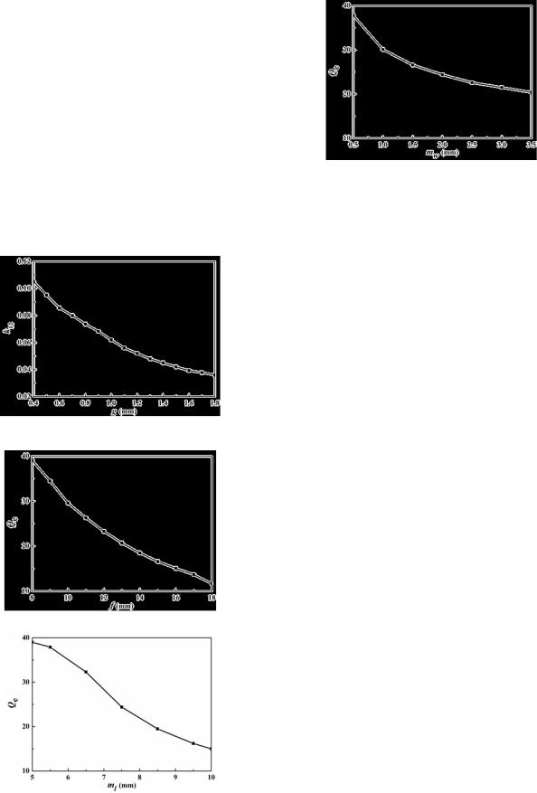
Fig. 4 Effects of key constructive parameters on external quality factor Qe; (a) Changing f with fixed ml=7.5mm and mw=2mm, (b) Changing ml with fixed f =12mm and mw=2mm, and (c) Changing mw with fixed f =12mm and ml=7.5mm.
The values of external quality factor denote the coupling strength between the HMSIRC resonator and the input port. In order to realize the required external quality factor, the GCPW is employed to feed the HMSIRC, and the coupling strength is mainly determined by the configurations of the GCPW coupling slots. The external quality factor can be evaluated by the formula as [19]
Qe = |
2π f0 |
τ |
(9) |
4 |
|
||
|
|
|
where f0 is the resonance frequency and τ is the group delay of the corresponding reflection coefficient.
The design curves of external quality factor are shown in Fig. 4. As shown in Fig. 4(a), the external quality factor deceases monotonically with the increase of insertion length, denoting that the larger the insertion length of the GCPW slots could make the external coupling stronger. In addition, as shown in Fig. 4(b), the ml has a significant influence on external quality factor Qe. The value of Qe decreases with the increase of ml. Similarly, the Qe decreases with the increase of mw but with smoother roll-off rate, as depicted in Fig. 4(c). Since the above three parameters have significant impact on the Qe, the desired value of Qe can be easily obtained by optimizing these parameters in the design process.
It can be concluded that, the anticipated bandpass filtering response could be achieved by properly adopting the dimensions of the physical structure according to the above theoretical and numerical analysis.
D. Two Radiation Nulls
Fig. 5 shows that, two radiation nulls can be achieved at both the upper and lower band-edges to improve the selectivity. In details, as is presented in Fig. 5(a), the location of the upper radiation null is affected by the gap width between the HMSIRC and the parasitic patch. As g decreases, the upper radiation null shifts to higher frequency, while the lower radiation null keeps unchanged. Likewise, as shown in Figs. 5 (b), the location of the lower radiation null can be controlled by altering the distance (d) of the shorting posts away from the center axis. When d increases, the lower radiation null shifts to a lower frequency and the upper radiation null is almost unaffected. Moreover, as observed in Fig. 5(c), the diameter of shorting posts has significant influence on the lower radiation null. The lower radiation null shifts towards lower frequency with the decrease of a value, leading to a smoother band-edge roll-off rate, and the suppression level increases at the same time. Especially, without the vias (when a = 0 mm), the out-of-phase current on the parasitic patch disappears, which results in
0018-926X (c) 2019 IEEE. Personal use is permitted, but republication/redistribution requires IEEE permission. See http://www.ieee.org/publications_standards/publications/rights/index.html for more information.

This article has been accepted for publication in a future issue of this journal, but has not been fully edited. Content may change prior to final publication. Citation information: DOI 10.1109/TAP.2019.2938574, IEEE Transactions on Antennas and Propagation
SUBMITTED TO THE IEEE TRANSACTIONS ON ANTENNAS AND PROPAGATION |
4 |
the lowest band-edge roll-off rate and the highest suppression level, as observed in Fig. 5(c). Here, taking the frequency selectivity and suppression level of lower stopband into account, the final design physical parameters a=1mm and d=10mm are selected, and its frequency selectivity and suppression level could satisfy the filtering standards of most practical applications [21], [22].
current directions on left and right sides of the parasitic patch are out-of-phase, making lower radiation null in Fig. 5(b).
(a)
(a)
(b)
(b)
(c)
Fig. 5 Influence of the key constructive parameters on the radiation nulls; (a) the gap width g, (b) the distance d, and (c) the diameter a.
In order to understand the operation mechanism of the radiation poles and two nulls, the current distributions on the parasitic patch and HMSIRC at center frequency, frequencies of the upper and lower radiation nulls are shown in Fig. 6. Clearly in Fig. 6(a), TM01 mode is well excited by the HMSIRC to make the parasitic patch operating as an effective radiator, as is anticipated in [23]. In Fig. 6(b), it is shown that, very weak currents are out-of-phase polarized on the HMSIRC and parasitic patch surfaces, which would cancel out each other’s contributions on the broadside radiation even though they are both low thus to form the upper radiation null, shown in Fig. 5(a). It is presented in Fig. 6(c) that, the current distribution is also very weak, and the
(c)
Fig. 6 Current distributions on the HMSIRC and parasitic patch at (a) operational center frequency, (b) upper radiation null frequency, and (c) lower radiation null frequency.
(a)
(b)
Fig. 7 (a) Three types of antennas (b) Comparison of simulated reflection coefficients and realized gains of the three types of antennas.
0018-926X (c) 2019 IEEE. Personal use is permitted, but republication/redistribution requires IEEE permission. See http://www.ieee.org/publications_standards/publications/rights/index.html for more information.

This article has been accepted for publication in a future issue of this journal, but has not been fully edited. Content may change prior to final publication. Citation information: DOI 10.1109/TAP.2019.2938574, IEEE Transactions on Antennas and Propagation
SUBMITTED TO THE IEEE TRANSACTIONS ON ANTENNAS AND PROPAGATION |
5 |
In order to demonstrate the advantages of our proposed filtenna, the three types of antennas, namely, radiating patch alone, HMSIRC alone and the proposed filtenna, are numerically investigated, and the results are provided in Fig. 7(a). The reflection coefficients, together with the corresponding realized gain values, as a function of the source frequency, are presented in Fig. 7(b). And the performance comparisons of the three type antennas are listed in Table. I. Clearly, the operating bandwidths for the patch alone and HMSIRC alone are quite narrow (1.9% and 1.1%), and the lower and upper band-edge roll-off rates for the corresponding realized gains are relatively poor (35dB/GHz, 20dB/GHz; 53dB/GHz, 21dB/GHz). By comparison, the proposed filtenna achieves a much wider operational bandwidth (5.1%) and a more stable passband gain response with the sharper band-edge roll-off rates (68dB/GHz, 233dB/GHz).
TABLE I. PERFORMANCE COMPARISON OF PATCH ALONE, HMSIRC ALONE,
AND OUR PROPOSED FILTENNA
|
FBW |
Lower |
Upper |
|
Selectivity |
Selectivity |
|
|
(%) |
||
|
(dB/GHz) |
(dB/GHz) |
|
|
|
||
Radiating patch alone |
1.9 |
35 |
20 |
|
|
|
|
HMSIRC alone |
1.1 |
53 |
21 |
|
|
|
|
Proposed filtenna |
5.1 |
68 |
233 |
|
|
|
|
purity were observed in both planes. The relatively low cross-polarization level is mainly ascribed to the parasitic patch, acting as a parasitic radiator, which is strictly symmetric with respect to both the E- and H-planes [24]. The measured co-polarized field at the broadside in both E- and H-planes is at least 30dB stronger than the corresponding cross-polarized counterpart. Because the simulated cross-polarization in E-plane is lower than -40dB, it was not plotted.
Fig. 9 Comparison of the measured and simulated reflection coefficients and the corresponding realized gains of the proposed filtenna.
III. EXPERIMENTAL RESULTS
The proposed filtenna was fabricated, installed, and measured, and the fabricated prototype is shown in Fig. 8. A 50-Ω SMA connector is used for measurement convenience.
Fig. 8 Photograph of the proposed filtenna. Left: top view. Right: bottom view.
A comparison of the simulated and measured reflection coefficients is presented in Fig. 9. The measured results demonstrate an impedance bandwidth (|S11|< -10dB, which could meet up with a common standard for practical engineering purposes [7, 11-12]) from 2.705 to 2.847 GHz, i.e., 142 MHz, giving FBW = 5.1%, which is 0.6 % larger than the simulated value. The measured results are reasonably in good agreement with their simulated values. The small discrepancy between the measured and simulated |S11| results can be attributed to the fabrication tolerances, which would lead to an inaccurate coupling strength between the HMSIRC and the parasitic patch, resulting in a slightly wider bandwidth.
The measured and simulated realized gain values at boresight direction are illustrated in Fig. 9. It can be seen that the realized gain curve is desirably flat across the entire passband. The maximum measured realized gain of 6.3 dBi is obtained, which is very close to the simulated value 6.8 dBi. The filtenna shows a good bandpass filtering response. Two radiation nulls, at 2.21 and 2.95GHz, are observed at the band-edges of boresight gain response, resulting in a sharp roll-off rate. The simulated and measured normalized radiation patterns in two principal cut planes at 2.77GHz are plotted in Fig. 10. Stable broadside radiation characteristics with very high polarization
(a) |
(b) |
Fig. 10 Simulated and measured radiation patterns of the proposed filtenna at 2.77 GHz; (a) in E-plane, and (b) in H-plane.
TABLE II. COMPARISONS OF THE DESIGN AND PERFORMANCE OF RECENTLY
REPORTED FILTENNAS AND THE PROPOSED FILTENNA
|
Num. |
Height |
Transverse |
Volume |
Num. of |
*Lower/ |
Real. |
|
|||
Ref. |
Upper |
FBW |
|||||||||
of |
(λ0) |
Size |
(λ0 |
3 |
) |
Radiation |
Selectivity |
Gain |
(%) |
||
|
layers |
(λ02) |
|
nulls |
(dBi) |
||||||
|
|
|
|
|
|
|
|
(dB/GHz) |
|
|
|
[9] |
3 |
0.33 |
0.279 |
0.092 |
0 |
96/55 |
6 |
5.5 |
|||
|
|
|
|
|
|
|
|
|
|||
[10] |
6 |
0.15 |
0.18 |
0.027 |
0 |
63/28 |
4.9 |
3 |
|||
|
|
|
|
|
|
|
|
|
|||
[11] |
2 |
0.08 |
0.825 |
0.066 |
2 |
26/57 |
6.79 |
1.56 |
|||
|
|
|
|
|
|
|
|
|
|||
[12] |
3 |
0.13 |
1 |
0.13 |
2 |
23/35 |
7.2 |
8.6 |
|||
|
|
|
|
|
|
|
|
|
|||
[13] |
2 |
0.03 |
0.4 |
0.012 |
0 |
103/85 |
6.73 |
6.3 |
|||
|
|
|
|
|
|
|
|
|
|||
[14] |
1 |
0.015 |
0.467 |
0.007 |
2 |
300/170 |
4.4 |
2.6 |
|||
|
|
|
|
|
|
|
|
|
|
|
|
This |
1 |
0.015 |
0.333 |
0.005 |
2 |
68/233 |
6.3 |
5.1 |
|||
work |
|||||||||||
|
|
|
|
|
|
|
|
|
|
||
*Selectivity value is calculated as (Rmax-Rmin)/|fmax-fmin|, where Rmax is the attenuation of the radiation null or 20dB attenuation from the maximum
realized gain if no radiation null, while Rmin is 3dB attenuation from that. fmax and fmin are their corresponding frequency points.
0018-926X (c) 2019 IEEE. Personal use is permitted, but republication/redistribution requires IEEE permission. See http://www.ieee.org/publications_standards/publications/rights/index.html for more information.
This article has been accepted for publication in a future issue of this journal, but has not been fully edited. Content may change prior to final publication. Citation information: DOI 10.1109/TAP.2019.2938574, IEEE Transactions on Antennas and Propagation
SUBMITTED TO THE IEEE TRANSACTIONS ON ANTENNAS AND PROPAGATION |
6 |
A comprehensive comparison of our proposed filtenna with the recently reported SIW filtenna designs in [9]-[14] is provided in Table II. In contrast with the complex multilayer SIW configurations reported in [9]-[13], our proposed single-layered filtenna could provide the comparable peak realized gain and operational bandwidth while maintaining the excellent out-of-band selectivity, even with much lower profile and smaller volume. Compared with the filtenna which employed single-layer SIW structure in [14], our filtenna, with the comparable profile and volume, can possess a nearly twice bandwidth and a higher realized gain. In addition, benefiting from the usage of half-mode technology, the transverse size of the proposed filtenna is smaller than the filtennas in [11]-[14]. Noted that, compared with the filtennas in [9-10], even the transverse size of our proposed filtenna is relatively larger than them, its profile is one-twentieth (one-tenth) of that in [9] ([10]), leading to the entire volume one-eighteenth (one-fifth) of that in [9] ([10]).
IV. CONCLUSION
A compact, single-layered SIW filtenna with parasitic patch was reported in this Communication. In the design, half-mode SIW technology was utilized to accomplish the filtenna compactness, and a parasitic patch was arranged close to HMSRIC so as to enhance the operational bandwidth and sharp the band-edge roll-off rate while maintaining ultra-low profile and small volume. The proposed compact filtenna offers the advantages of low cost and simple configuration with wideband, high-gain and stable in-band radiation performance characteristics and excellent out-of-band selectivity. These advantages empower it very suitable for practical applications in many wireless mobile space-limited platforms.
REFERENCES
[1]D. Deslandes and K. Wu, “Integrated microstrip and rectangular waveguide in planar form,” IEEE Microw. Wireless Compon. Lett., vol. 11, no. 2, pp. 68–70, Feb. 2001.
[2]Y. Cassivi, L. Perregrini, P. Bressan, K. Wu, and G. Conciauro, “Dispersion characteristics of substrate integrated rectangular waveguide,” IEEE Microw. Compon. Lett., vol. 12, no. 2, pp. 333–335, Feb. 2002.
[3]G. Q. Luo, Z. F. Hu, W. J. Li, X. H. Zhang, L. L. Sun, and J. F. Zheng, “Bandwidth-enhanced low-profile cavity-backed slot antenna by using hybrid SIW cavity modes,” IEEE Trans. Antennas Propag., vol. 60, no. 4, pp. 1698–1704, Apr. 2012.
[4]K. Zhou, C.-X. Zhou, and W. Wu, “Resonance characteristics of substrate-integrated rectangular cavity and their applications to dual-band and wide-stopband bandpass filters design,” IEEE Trans. Microw. Theory Techn., vol. 65, no. 5, pp. 1511–1524, May 2017.
[5]T. Zhang, W. Hong, Y. Zhang, and K. Wu, “Design and analysis of SIW cavity backed dual-band antennas with a dual-mode triangular-ring slot,” IEEE Trans. Antennas Propag., vol. 62, no. 10, pp. 5007–5016, Oct. 2014.
[6]X. Y. Zhang, W. Duan, and Y.-M. Pan, “High-gain filtering patch antenna without extra circuit,” IEEE Trans. Antennas Propag., vol. 63, no. 12, pp. 5883–5888, Dec. 2015.
[7]C.-K. Lin and S.-J. Chung, “A compact filtering microstrip antenna with quasi-elliptic broadside antenna gain response,” IEEE Antennas Wireless Propag. Lett., vol. 10, pp. 381–384, Apr. 2011.
[8]M. -C. Tang, Y. Chen, and R. W. Ziolkowski, “Experimentally validated, planar, wideband, electrically small, monopole filtennas based on capacitively loaded loop resonators,” IEEE Trans. Antennas Propag., vol. 64, no. 8, pp. 3353–3360, Aug. 2016.
[9]H. T. Cheng, Y. Yusuf, and X. Gong, “Vertically integrated three-pole filter/antennas for array applications,” IEEE Antennas Wireless Propag. Lett., vol. 10, pp. 278–281, Apr. 2011.
[10]Y. Yusuf, H. T. Cheng, and X. Gong, “A seamless integration of 3-D vertical filters with highly efficient slot antennas,” IEEE Trans. Antennas Propag., vol. 59, no. 11, pp. 4016–4022, Nov. 2011.
[11]H. Chu, C. Jin, J. X. Chen, and Y. X. Guo, “A 3-D millimeter-wave filtering antenna with high selectivity and low cross-polarization,” IEEE Trans. Antennas Propag., vol. 63, no. 5, pp. 2375–2380, May 2015.
[12]K. Xu, J. Shi, X. Qing, and Z. N. Chen, “A substrate integrated cavity backed filtering slot antenna stacked with a patch for frequency selectivity enhancement,” IEEE Antennas Wireless Propag. Lett., vol. 17, no. 10, pp. 1910–1914, Oct. 2018.
[13]K. -Z. Hu, M. -C. Tang, M. Li, and R. W. Ziolkowski, “Compact, low-profile, bandwidth-enhanced substrate integrated waveguide filtenna,” IEEE Antennas Wireless Propag. Lett., vol. 17, no. 8, pp. 1552–1556, Aug. 2018.
[14]K. Dhwaj, J. M. Kovitz, H. Tian, L. J. Jiang, and T. Itoh, “Half-mode cavity based planar filtering antenna with controllable transmission zeroes,” IEEE Antennas Wireless Propag. Lett., vol. 17, no. 5, pp. 833–836, May 2018.
[15]Y. Q. Wang, W. Hong, Y. D. Dong, B. Liu, H. J. Tang, J. X. Chen, X. X. Yin, and K. Wu, “Half mode substrate integrated waveguide (HMSIW) filter,” IEEE Microw. Wireless Comput. Lett., vol. 17, no. 4, pp. 265–267, Apr. 2007.
[16]K. Zhou, C.-X. Zhou, and W. Wu, “Dual-mode characteristics of half-mode SIW rectangular cavity and applications to dual-band filters with widely separated passbands,” IEEE Trans. Microw. Theory Techn., vol. 66, no. 11, pp. 4820–4829, Nov. 2018.
[17]Q. Lai, C. Fumeaux, W. Hong, and R. Vahldieck, “Characterization of the propagation properties of the half-mode substrate integrated waveguide,” IEEE Trans. Microw. Theory Tech., vol. 57, no. 8, pp. 1996–2004, Aug. 2009.
[18]C.-K. Lin and S.-J. Chung, “A filtering microstrip antenna array,” IEEE Trans. Microw. Theory Techn., vol. 59, no. 11, pp. 2856–2863, Nov.2011.
[19]J. S. Hong and M. J. Lancaster, Microstrip Filter for RF/Microwave Applications. New York, NY, USA: Wiley, 2001.
[20]C. A. Balanis, Antenna Theory: Analysis and Design, 3rd ed. New York, NY, USA: Wiley, 2005.
[21]G.-H. Sun, S.-W. Wong, L. Zhu, and Q.-X. Chu, “A compact printed filtering antenna with good suppression of upper harmonic band,” IEEE Antennas Wireless Propag. Lett., vol. 15, pp. 1349–1352, 2016.
[22]C. F. Ding, X. Y. Zhang, Y. Zhang, Y. M. Pan, and Q. Xue, “Compact broadband dual-polarized filtering dipole antenna with high selectivity for base-station applications,” IEEE Trans. Antennas Propag., vol. 66, no. 11, pp. 5747–5756, Nov. 2018.
[23]L. Sun, G. Zhang, B.-H. Sun, W.-D. Tang, and J.-P. Yuan, “A single patch antenna with broadside and conical radiation patterns for 3G/4G pattern diversity,” IEEE Antennas Wireless Propag. Lett., vol. 15, pp. 433–436, 2016.
[24]M.-C. Tang, S. Xiao, T. Deng, H. Zhu, and B.-Z. Wang, “Design of compact, low-profile, wideband, dual-frequency patch antennas based on complementary co-directional SRRs,” IEEE Antennas and Propag. Mag., vol. 56, no. 6, pp. 72-89, December 2014.
0018-926X (c) 2019 IEEE. Personal use is permitted, but republication/redistribution requires IEEE permission. See http://www.ieee.org/publications_standards/publications/rights/index.html for more information.