

диафрагмированные волноводные фильтры / 465abec2-98dd-4937-88e5-c6fc30b269a0
.pdf174 |
IEEE TRANSACTIONS ON ANTENNAS AND PROPAGATION, VOL. 63, NO. 1, JANUARY 2015 |
Low-Profile Slot Transmitarray Antenna
Bahman Rahmati and Hamid R. Hassani
Abstract—A novel ultrathin slot-based transmitarray antenna is presented. The related unit cell consists of two thin dielectric layers placed on top of each other, with annular ring slots placed on the outer layers and a PBG element placed on the common interface. The combination of the two annular ring slots and the PBG element acts as a bandpass filter for the transmitted wave. The design of the elements can be carried out through a simple circuit-based analysis approach. The proposed two-layer structure, the unit cell, has a thickness of 


 and provides the required 360
 of phase
shift. Furthermore, over the bandwidth, the unit cell can have up to 7 of phase error for incident angles of up to 50
 . The unit cell and the full transmitarray prototype are fabricated, and the results were compared with simulation and discussed. The full transmitarray has 1 dB gain bandwidth of 5.7% and efficiency of 38% at the center frequency. The structure is simulated via HFSS and CST software package.
Index Terms—Antenna array, lens antenna, microstrip array, reflectarray, transmitarray.
I. INTRODUCTION
I N wireless technology, in the area of antenna, the need for low-profile, lightweight, low-cost, broadband, and high-gain antennas has increased recently. Among the possible options, the transmitarray antenna is a promising potential
technology to meet these requirements.
Comprising a planar array of printed elements, the transmitarray avoids the fabrication complexity inherent in parabolic reflectors, and being usually less than one wavelength thick, it has size and weight advantages over shaped dielectric lenses. Free-space feeding improves the radiation efficiency by eliminating the losses that occur with corporate feed networks of a large planar array of printed elements. In a reflectarray with the feed being in front of the array aperture, the efficiency is reduced because of feed blockage losses, whereas in a transmitarray, because the feed is placed on the opposite side of the array, the blockage does not exist.
To form a pencil beam in transmitarray design, the phase shifts from the source to the transmitarray elements and, subsequently, to a planar surface must be equal for the wave beams on a planar surface before the aperture. Transmitarray collimates an incident wave by manipulating the phase shifts at different positions on the planar surface. To produce arbitrary phases on
Manuscript received April 15, 2014; revised August 05, 2014; accepted October 07, 2014. Date of publication November 07, 2014; date of current version December 31, 2014.
The authors are with the Electrical & Electronic Engineering Department, Shahed University, Persian Gulf Highway, Tehran, Iran (e-mail: brahmati@shahed.ac.ir; hassani@shahed.ac.ir).
Color versions of one or more of the figures in this paper are available online at http://ieeexplore.ieee.org.
Digital Object Identifier 10.1109/TAP.2014.2368576
the aperture, at least 360 of phase range is required. The magnitude of transmission is an additional design consideration for transmitarray elements. In addition to a large phase range, large bandwidth, low reflection, low insertion loss, and small physical profile are also desirable.
Up-to-date transmitarray antennas have been designed using multiple dielectric layers with printed patch antennas on each layer. The designs are through two approaches: the layered scatterer approach (LS) and the guided-wave approach (GW).
In the LS approach, the required phase shift for each array element is achieved by varying the element dimensions. Multiple dielectric layers with printed patch antennas on each layer are coupled through slots in the ground plane of the patches [1]–[3], air gap layers [4], [5], or printed cross-elements [6] controlling the level of coupling between the two patches, resulting in a unit cell acting as a spatial phase shifter. In the case of [1] and [2], unit cells that have 


 and
and 


 thicknesses, respectively,
were proposed. The transmitarray of [3] provides 7% bandwidth with a thickness of 


 . The transmitarrays of [4] and [5]
that use coupled patch rings on a 4-dielectric layered structure (approximately 

 thick) provides 1 dB gain bandwidth of
7.5%. The unit cell described in [6] uses four dielectric layers, with each layer having a thickness of 


 . A full review of
the various phase-shifting surfaces developed in recent years is reported in [7].
In the guided-wave approach, the required phase shift for each element is achieved through a physical phase shifter, whereas the element dimensions are kept constant throughout the array. Two dielectric substrates are separated from each other by a middle layer. Two patch antennas are on the outer layer of the substrates, and either a simple printed transmission line phase shifter [8], [9] or a circuit-based phase shifter [10], [11] connecting the two patches physically, is on the middle layer. In [10], a unit cell with an overall thickness of 


 is
is
given, whereas in [11], a thick transmitarray design providing 5.8% of the bandwidth is described.
A summary of comparison between previously reported transmitarray designs is presented in Table I. In the above-men- tioned works related to the LS and GW approaches, the required phase shift that can be achieved from a unit cell typically requires at least three dielectric substrates, making the overall antenna structure thick and expensive.
To minimize the overall transmitarray antenna thickness, while keeping the bandwidth almost similar to the previously reported wideband structures, this paper uses the LS approach and presents a new design based on slot elements that provides the required phase range with less number of dielectric layers. The unit cell comprises two dielectric layers with annular ring slots on the outer layers and a uniplanar compact photonic bandgap (UC-PBG) element on the inner layer that acts as
0018-926X © 2014 IEEE. Personal use is permitted, but republication/redistribution requires IEEE permission. See http://www.ieee.org/publications_standards/publications/rights/index.html for more information.

RAHMATI AND HASSANI: LOW-PROFILE SLOT TRANSMITARRAY ANTENNA |
175 |
TABLE I
COMPARISON BETWEEN REPORTED TRANSMITARRAY ANTENNAS UC = UNIT
CELL, LS = LAYERED SCATTERER, GW = GUIDED WAVE
Fig. 1. Unit cell configuration and its equivalent circuit: (a) annular ring slot resonant element on a dielectric substrate, (b) UC-PBG coupling/resonant element, and (c) the two-layered structure.
Fig. 2. Simulated transmission coefficients (magnitude and phase) and ADS equivalent circuit response of an annular ring slot resonant element, Fig. 1a, for various slot gaps,  (
(


 and
and 


 ).
).
Fig. 3. Simulated transmission coefficients (magnitude and phase) of an annular ring slot resonant element for various slot side lengths, 


 (
(


 and
and 


 ).
).
the coupler and as an additional resonator. In the following sections, the design of a thin two-layer slot transmitarray unit cell providing 360 of phase shift along with the transmitarray is provided. The design is shown to be easily extendable to larger number of layers providing a multiple of 360
 of phase shift.
II. UNIT CELL DESIGN
In this section, the design of the proposed slot transmitarray unit cell is provided, the structure of which, is shown in Fig. 1. Thin unit cell with minimum number of layers to achieve the desired phase shift is the main goal of this unit cell design. Accordingly, the overall design is based on a pair of annular slot ring elements, each is replaced on the outer surface of two attached dielectric substrates, and a printed PBG element is on the inner surface of the substrates. The PBG acting as a resonant/coupler element reduces the requirement of extra layer. Parametric studies of dimensions of the annular slot and a study of different coupling element types to provide a compact unit cell with the proper range of phase shift angles are provided. The dielectric substrates used in this paper are RO4003 with a permittivity of 3.55 and a thickness of 0.8 mm.
A. Annular Ring Slot Element
It is known that a slot antenna element can provide a low-pro- file, lightweight, low-cost, and broad bandwidth. As such, in the design of a transmitarray, one can use slot element rather than the usual printed patch element to provide wave transmission with the least possible loss and with the maximum amount of phase shift. For this purpose, a very simple annular ring slot can be selected that would allow wave transmission and provide the required phase shift.
For the simple single-layer annular ring slot chosen in this work, Fig. 1a, the transmission magnitude and phase are plotted in Figs. 2 and 3 for various slot gaps and slot side lengths. In doing so, when one parameter is changed, the other parameters of the slot are kept constant.
For the above single-layer annular ring slot, to have knowledge of the overall phase response and the passband behavior, a simple model based on a parallel-type LC circuit [Fig. 1(a)] that can provide similar results to that of the full-wave results can be introduced. Fig. 2 also shows the transmission magnitude and phase of the single annular ring slot based on the equivalent LC model as obtained through Advanced Design System (ADS) package. As can be seen, the CST simulation and the model results are very close to each other for both narrow and wide slots.

176 |
IEEE TRANSACTIONS ON ANTENNAS AND PROPAGATION, VOL. 63, NO. 1, JANUARY 2015 |
TABLE II
EQUIVALENT LC MODEL PARAMETER VALUES FOR THE UNIT CELL OF FIG. 1(A)
FOR VARIOUS GAP SIZES G
In obtaining such close results, the quality factor (QC and QL) of the lumped elements should also be taken into account. Table II provides the relevant equivalent model parameter values.
From the simulated results shown in Fig. 2, it is seen that by increasing the slot gap, G, the passband center frequency and bandwidth of the transmission coefficient, S21, increases. Also shown in Fig. 2 are the simulated transmission phases for various slot gaps G. The transmission phase changes from 45 to 


 within the 3-dB passband (overall 90
 of phase shift). Thus, with an increase in the annular slot gap, both center frequency and bandwidth of the phase response increases.
Although larger slot gaps can provide a higher bandwidth, to have the antenna center frequency in the desired X band, results show that a slot gap of 0.5 mm provides the appropriate response. In the following work, this slot gap is kept constant.
Fig. 3 shows the transmission response of the annular ringslot element for various slot side lengths, 


 . It is seen that with the increase in side length, the passband center frequency decreases, whereas its bandwidth does not change. A comparison between the phase responses shows that the change in slot side length leads to curves that are almost parallel to each other. This is a desirable feature that can be used in the design of transmitarray elements with various phase responses.
B. Single Dielectric Layer with Stacked Annular Ring Slot Elements
Because the single annular ring slot element provides only 90 of phase shift, one needs to modify this slot element to provide 360
 of desired phase response.
By considering the equivalent circuit of the single slot element, shown in Fig. 1(a), one expects to have higher phase response (up to double) if two such parallel resonance circuits are simply coupled to each other. A simple way to provide the coupling is to place the two annular ring slots on top of each other. If appropriate spacing is used in between these two layers, one can double the phase shift offered by each slot alone. This technique was used in [5], [6] by stacking patch elements (using several dielectric layers) to obtain higher phase shifts.
The response of the single dielectric layer stacked annular ring slot elements is shown in Fig. 4. From these results, one can notice that when the slot separation is lower than one wavelength, 


 , the two resonant slots behave like a single slot element providing the same 90
 phase response. By increasing the separation between the two slots and thus changing the level of the coupling between the two slots, one can increase the overall phase shift. After a specific separation between the two slot layers, one can obtain twice the single element phase
Fig. 4. Simulated transmission coefficients (magnitude and phase) of the single dielectric layer with stacked annular ring slots for various substrate thicknesses,  (
(


 and
and 


 ). ADS model parameters:
|
|
|
|
|
|
|
|
|
|
|
|
|
|
|
; |
|
|
|
|
|
|
|
|
|
|
|
|
|
|
|
; |
|
|
|
|
|
|
|
|
|
|
|
|
|
|
|
; |
|
|
|
|
|
|
|
|
|
|
|
|
|
|
|
. |
|
|
|
|
|
|
|
|
|
|
|
|
|
|
|
|
|
Fig. 5. Equivalent circuit model for the stacked single-layer annular ring slot unit cell.
shift, that is, 180 ; however, such an increase in the separation between the layers makes the magnitude response more undesirable.
By exporting the relevant touchstone parameters of the CST simulation of the single annular ring slot, the single-layer stacked slot unit cell can be simulated through ADS. To have results similar to the full-wave ones, one requires having a transmission line equivalent circuit in parallel with a transmission zero in between the touchstone parameters of the annular ring slots.
The equivalent circuit model of the stacked annular ring slots is shown in Fig. 5. The need for the transmission line equivalent circuit, CSS and LSS, is due to the coupling provided by the substrate, and the transmission zero is related to the dimension of the slot. The transmission zero that is modeled with LZSS and CZSS creates one notch in the magnitude response, and the transmission line model couples the two slot resonators together. As can be seen from the results shown in Fig. 4, this model can provide a good and fast knowledge of the overall phase response as well as the passband behavior of a stacked annular ring slot using only the single annular ring slot results.
To have up to 360 phase response, one needs to increase the number of the stacked annular ring slots to four (three dielectric layers), which makes the overall structure not compact. In Fig. 4, because the height of the single-layer stacked slots is 0.4 mm or


 at 10 GHz, the height of the three-layer stacked slots would be 1.2 mm. The work regarding the stacked patches reported in [5] used a patch separation of


 , where
 is the free space wavelength at the center frequency of operation. In this paper, the stacked slots have a separation of


 , which is lower than that of [5].

RAHMATI AND HASSANI: LOW-PROFILE SLOT TRANSMITARRAY ANTENNA
Fig. 6. Simulated transmission coefficients (magnitude and phase) of two-layer structure with annular ring slots in the outer layers and cross-type element in the
middle layer for various cross-strip widths, |
|
|
|
|
( |
|
|
|
|
|
|
|
|
|
|
|
|
, |
|
|
|
|
|
|
|
|
|
|
|
, |
||||||||||||||||||||||||||||
|
|
|
|
|
|
|
|
|
|
|
|
|
|
|
|
|
|
, and |
|
|
|
|
|
|
|
|
|
|
|
|
|
|
|
|
). |
|
|
|
|
|
|
|
|
|
|
|
|
|
|
|
|
|
|
|
|
|
||
177
Fig. 7. The equivalent circuit model of the two-layered annular ring slots with a UC-PBG in the middle layer.
To have a better control on the unit cell magnitude and phase response at a fixed separation between the slots, one needs to change the coupling method between the two slots. A cross-type printed element can be introduced in between the two stacked slots, as shown in the legend of Fig. 6. Based on the work reported in [6], if two resonators are coupled through a cross-type printed element, the cross-coupler can be viewed as a series capacitance between the two resonators. The effective capacitance (
 in Fig. 5) can be used to improve the unit cell performance. Relevant results for various cross-element widths,
  , are shown in Fig. 6.
C. Two Dielectric Layer Stacked Slot Elements with UC-PBG Coupler
The stacked slot elements of the previous section with crosstype coupler in between do not lead to an increase in the phase shift when compared with the two stacked slot resonators. As reported in the literature, to increase the phase shift, one needs to increase the number of resonances, usually up to 4 to obtain 360 . For maintaining the structure with two dielectric layers, a resonator in between the two stacked slot elements (instead of the capacitive cross-element of previous section) that can act both as a coupler and as an additional resonator is proposed here. This resonator should be of printed type and simple to design and should act as a series parallel-type resonance in between the two parallel resonances of the two slots, as shown in Fig. 7. The simple cross of the previous section can only provide a capacitive coupling. To provide an extra resonance, the cross should be modified. A patch-type shape is introduced into the cross-element for this purpose. The size of the patch


 is chosen in such a way that it provides a resonance near that of the slot resonance and the required coupling (flat amplitude response over the bandwidth) in between the slot and the patch. This patch is connected to the neighboring patches through narrow strip lines. The patch surface provides the capacitive, whereas the strip lines provide the inductive effect of the created resonance.
To be able to have a better control on the resonant frequency and the coupling effect, small square elements are cut off from the patch along the axis with parameters GC and LL, as shown
Fig. 8. Simulated transmission coefficients (magnitude |
|
and phase) of |
||||||||||||||||
UC-PBG-type coupled element for various stub lengths |
|
|
|
( |
|
|
|
|
|
|
|
|||||||
|
|
|
|
|
|
|
). |
|
|
|
|
|
|
|
|
|
|
|
|
|
|
|
|
|
|
|
|
|
|
|
|
|
|
|
|||
in Fig. 1(b). Increase in GC reduces the patch surface, thus increasing the resonant frequency of the patch element, whereas increasing LL increases the inductive effect of the resonance, reducing the resonant frequency, as shown in Fig. 8. This coupling resonator can be named as a UC-PBG [12], [13] structure. Through a full-wave simulation and an equivalent circuit in the ADS software, one can show that the UC-PBG behaves as a parallel type of resonance with series-type coupling capacitors [Fig. 1(b)]. As will be shown in the following, with this UC-PBG element in between the two annular slots, one can provide the desired 360 of phase change from a two-layer unit cell.
The structure of the proposed two-layer unit cell is shown in Fig. 7 along with its equivalent circuit. The three parallel-type resonators are coupled through series capacitors 

 (capacitance effect between PBG and slot) and

 (capacitance effect due to substrate).
To be able to design the overall unit cell, the following procedure can be applied. Our aim is to design a two-layer transmit array unit cell (two slots and a UC-PBG element) with three near resonances as well as optimum coupling between them, leading to flat magnitude response and maximum phase change over the desired frequency band.
The center frequency of the annular ring slot resonance is dependent on the slot side length 
 and slot gap size
  , whereas
178 |
IEEE TRANSACTIONS ON ANTENNAS AND PROPAGATION, VOL. 63, NO. 1, JANUARY 2015 |
TABLE III
PARAMETER VALUES RELATED TO (1) AND (2)
the center frequency of the UC-PBG resonance depends on parameters such as  ,
, 
 ,
,  , and
, and 
 (the parameters with C subscript relate to the capacitance, and those with L subscript relate to the inductance of the resonance). Because there are various parameters of the slot and UC-PBG that control the resonances, to simplify the analysis, one can consider some parameters to be constant,


 ,
, 


 (simulation shows that changes in these two parameters do not have a significant effect). For the UC-PBG, there are two more parameters left, LL and WC. The relation between these two parameters and those of the slot should be chosen in such a way that the UC-PBG resonance would be near to that of the slot.
In the previous discussion, the required resonance is obtained without considering the required coupling. To obtain the required coupling, parameters 
 and
and 
 should be adjusted. In doing so, the resonance frequency of the UC-PBG also changes.
Through a parametric study, one can obtain a relation, equations (1) and (2), between the UC-PBG and the slot parameters to reach the desired response, flat magnitude, and maximum phase change over the bandwidth. The related coefficients are shown in Table III
(1)
(2)
These relations have been obtained for a dielectric thickness of 


 . In the following sections, the above-mentioned relations are applied.
D. Unit Cell Results and Discussion
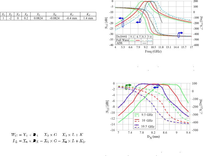
The proposed structure of the two-layered stacked annular ring slot elements with UC-PBG coupler in between based on parameters according to equations (1) and (2) is simulated, and the response is shown in Fig. 9 for various 
 , the slot side length. Results show that by setting the
 parameter to any value shown in the legend of Fig. 9, the desired phase shift over the required bandwidth can be obtained. Fig. 9 also shows the transmission magnitude and phase of the equivalent LC model of Fig. 7, for the two-layered annular ring slots with a UC-PBG element in the middle as obtained through ADS. As can be seen in Fig. 9, this model is not exact but can provide a good and fast knowledge of the overall phase response and the passband behavior of the relevant unit cell.
To obtain a clearer picture of the behavior of the phase shift response, Fig. 10 is shown for the three frequencies of 9.5, 10, and 10.5 GHz. It can be seen that for a given frequency, by changing the slot side length DX, one can obtain more than 360 of phase shift over the 3-dB magnitude bandwidth. As mentioned previously, because of having a parallel phase response between the curves shown in Figs. 9 and 10, one can expect to have a wideband transmitarray from such a structure. The insertion loss of the proposed unit cell does not vary by
Fig. 9. Simulated transmission coefficients (magnitude and phase) of the twolayered annular ring slots with a UC-PBG element in the middle for various slot
side lengths |
|
|
|
( |
|
|
|
|
|
|
|
|
|
|
|
|
|
, |
|
|
|
|
|
|
|
|
|
|
|
|
|
|
|
|
|
, and |
|
|
|
|
|
|
|
|
|
|
|
|
|
|
|
|
|
|
|
|
|
|
|
|
|
|
|
|
|
|
). |
||||||||||||||||
|
|
|
|
|
|
|
|
|
|
|
|
|
|
|
|
||||||||||||||||||||||||||||||||||||||||||||||||||||||||||||||||||||
ADS model parameters: |
|
|
|
|
|
|
|
|
|
|
|
|
|
|
|
|
; |
|
|
|
|
|
|
|
|
|
|
|
|
|
|
; |
|
|
|
|
|
|
|
|
|
|
|
|
|
|
; |
||||||||||||||||||||||||||||||||||||
|
|
|
|
|
|
|
|
|
|
|
|
|
|
||||||||||||||||||||||||||||||||||||||||||||||||||||||||||||||||||||||
|
|
|
|
|
|
|
|
|
|
; |
|
|
|
|
|
|
|
|
|
|
; |
|
|
|
|
|
|
|
|
|
|
|
|
|
|
|
|
|
. |
|
|
|
|
|
|
|
|
|
|
|
|
|
|
|
|
|
|
|
|
|
|
|
|
|
|
|
|
|
|
|
|
|
|
|
|
|
|
||||||
Fig. 10. Simulated transmission coefficients (magnitude and phase) of the twolayered annular ring slots with a UC-PBG element in the middle for various slot
side lengths |
|
|
|
|
|
at three frequencies ( |
|
|
|
|
|
|
|
|
|
|
|
|
|
|
|
|
|
|
, |
|
|
|
|
|
|
|
|
|
|
|
, |
|
|
|
|
|
|
|
||||||||||||||||||||||
|
|
|
|
|
|
|
|
|
|
|
|
|||||||||||||||||||||||||||||||||||||||||||||||||||||||
|
|
|
|
|
|
|
, |
|
|
|
|
|
|
|
|
|
|
|
|
|
|
|
|
, and |
|
|
|
|
|
|
|
|
|
|
|
|
). |
|
|
|
|
|
|
|
|
|
|
|
|
|
|
|
|
|
|
|
|
|
||||||||
|
|
|
|
|
|
|
|
|
|
|
|
|
|
|
|
|
|
|
|
|
|
|
|
|
|
|
|
|
|
|
|
|
|
|
|
|
|
|
|
|
|
|
|
|
||||||||||||||||||||||
more than 3 dB in the frequency range of phase change from 0 to 360
 , which is equivalent to a transmission fractional bandwidth of 18%.
The phase response obtained above is for normal incidence. Fig. 11 shows the transmission coefficient magnitude and phase responses of the proposed unit cell for various angles of incidence at three frequencies. It is seen that the unit cell can create a maximum of 7 of phase error for incident angles up to 50
 . This makes the proposed unit cell a good candidate for transmitarrays even with low

 ratios of 0.42. The error value for F/D ratio of 0.8 or, in other words, for incident angles up to 32
 is lower than 3
 . A phase error of 7
 is equivalent to a reduction of 0.065 dB in directivity [14].
The proposed transmitarray unit cell is fabricated on Rogers RO4003 and placed in between two WR90 rectangular waveguides and tested. For a 


 mode traveling in a WR90 standard waveguide at 10 GHz, according to waveguide simulator theory, an off-broadside illumination should be assumed with a wave propagation angle of 41
 in the H-plane.
To measure the characteristics of the unit cell, it is required to place two elements side by side within the waveguide to be suitable for the WR90, as shown in the legend of Fig. 12. This test environment simulates a plane wave that is incident on an

RAHMATI AND HASSANI: LOW-PROFILE SLOT TRANSMITARRAY ANTENNA |
179 |
Fig. 11. Simulated transmission coefficients (magnitude and phase) of the two- |
|||
layer annular ring slots with a UC-PBG element in the middle layer for various |
|||
incident angles at three frequencies ( |
, |
, |
|
, |
, |
, and |
). |
Fig. 13. (a) Equivalent circuit of a four-layered unit cell and (b) simulated |
|||||
transmission coefficients (magnitude and phase) of the twoand four-layered |
|||||
unit cells ( |
, |
|
, |
|
, |
, |
|
, and |
|
). ADS model param- |
|
eters: |
; |
; |
; |
|
; |
; |
; |
; |
|
; |
. |
Fig. 12. Simulated and measured transmission coefficients (magnitude and phase) of the proposed two-element unit cell in waveguide and PBC envi-
ronment with parameters: |
|
|
|
|
|
|
|
|
|
|
|
|
|
|
|
|
|
|
|
|
; |
|
|
|
|
|
|
|
|
|
|
|
|
|
|
|
|
|
|
|
|
|
|
; |
|
|
|
|
|
|
|
|
|
|
|
|
|
; |
||||||||||||||||||||
|
|
|
|
|
|
|
|
|
|
|
|
|
|
|
; |
|
|
|
|
|
|
|
|
|
|
|
|
|
|
; |
|
|
|
|
|
|
|
|
|
|
|
|
|
|
|
|
. |
|
|
|
|
|
|
|
|
|
|
|
|
|
|
|
|
|||||||||||||||
infinite array, where the vertical and horizontal periods are set by the waveguide dimension [15]. Similar to the measurement procedure, the two-element unit cells are also placed in between two rectangular waveguides, and the structure is simulated. The relevant measured and simulated 


 parameters of the structure are shown in Fig. 12. Also shown in this figure is the simulation result of the unit cell with two elements placed side by side in a periodic boundary condition, PBC (without the use of the waveguides) with an incident angle of 0
 . The difference between the results of the waveguide simulator and that of the PBC are due to the difference between the free space and the waveguide impedances and the incidence angles, zero in the free space and 41
 in the waveguide simulator (as shown in Fig. 11).
As can be seen in Fig. 12, if 


 varies by less than 3 dB, results show that a two-layer unit cell can provide 360
 of phase range.
To increase the phase change of the proposed unit cell, one can double the number of layers. Fig. 13a shows the equivalent circuit of a four-layered transmitarray unit cell. It should be noted that, in the four-layer structure, because the middle-layer annular ring slot is covered from both sides with dielectrics (when compared with the slots in the outer layers), the coupling between this element and the UC-PBG element slightly
changes, when compared with that of the two-layer case; as such, one needs to modify this middle-layer annular ring slot side length, 

 , and the distance between this layer and UC-PBG layer,
 , to achieve a flat magnitude and maximum phase response over the bandwidth. Equations (1) and (2) still apply.
Fig. 13(b) shows the transmission coefficients of a four-lay- ered structure (three stacked slots with two UC-PBG elements in between) when compared with that of a two-layer structure. It is seen that the phase change of the transmission coefficient in the four-layer structure is double (720 ) that of the two-layer structure (360
 ). Fig. 13(b) also shows the transmission magnitude and phase of the equivalent LC model. As can be seen, this model provides an approximate knowledge of the overall phase response as well as the passband behavior of the relevant unit cell.
III. TRANSMITARRAY OF ANNULAR RING SLOTS WITH
UC-PBG IN BETWEEN
The proposed unit cells of the previous section are incorporated into a transmitarray, shown in Fig. 14. The array is designed for operation at a center frequency of 9.7 GHz. The transmitarray is designed on RO4003 substrate, and the elements, which have fixed geometrical parameters, are listed as follows:


 ;
; 


 ;
; 


 ;
; 


 ;
; 


 . For each element of the array, the required phase (the phase shift to compensate the spatial delay between the feed and the array surface) is obtained through appropriate


 length, and the PBG parameters are then calculated from (1) and (2).
180 |
IEEE TRANSACTIONS ON ANTENNAS AND PROPAGATION, VOL. 63, NO. 1, JANUARY 2015 |
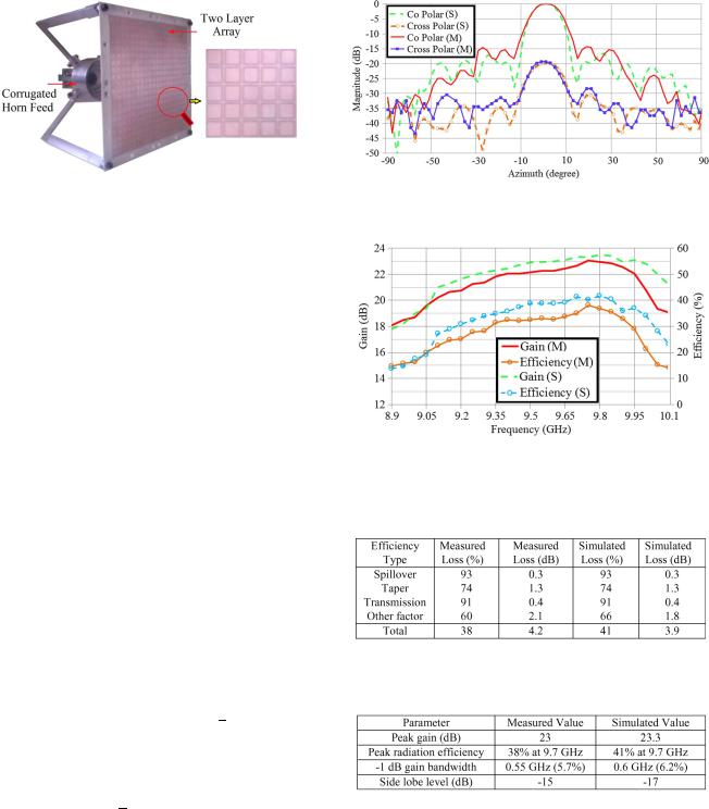
Fig. 14. Geometry of transmitarray with 400 elements.
Fig. 15. Measured and simulated E-plane radiation pattern of the 20  20 elements of the transmitarray antenna at a center frequency of 9.7 GHz.
A. Design of the Transmitarray
The transmitarray design includes two parts, the feed antenna and the printed array.
For the feed antenna, an X band optimum corrugated horn is used with low cross polarization ( 26 dB) and equal E- and H-plane patterns. The horn has a gain of 15.5 dB at 9.7 GHz, and its pattern can be modeled by a 


 . The horn antenna, including the coaxial to the waveguide adaptor, has a return loss of better than 19 dB over the X-band.
The horn antenna is placed in line with the center of the array. The focal-length-to-diameter ratio (F/D) of the transmitarray antenna is chosen to be 0.8. The transmitarray has 20  20 of the proposed unit cells that fill the 192
  192 mm aperture. Each unit cell’s dimension is selected to provide the appropriate phase shift distribution across the array. As shown in Fig. 14, a rigid frame is used to mount both the array and the feed for anechoic chamber measurements.
B. Transmitarray Results and Discussion
Ansoft HFSS software package is used to simulate both the feed horn and the entire transmitarray elements.
Fig. 15 shows the measured coand cross-polar far-field |
|
E-plane radiation patterns of the transmitarray at a center fre- |
|
quency of 9.7 GHz. Although not shown, the measured H-plane |
|
pattern is similar to that of the E-plane pattern. Because no |
|
amplitude tapering is considered in this paper, the figure shows |
|
that the side-lobe level is approximately |
17 dB below the |
main peak. Also, the cross-polar field of |
the transmitarray |
in the bore sight is below |
|
|
19 dB, which is the same as the |
|
|
|
|||
feed cross-polar level of |
|
|
19 dB. Simulated and measured |
|
|
|
|||
peak gain versus frequency is shown in Fig. 16. This figure shows that the measured 1 dB gain bandwidth achieved by this transmitarray antenna is 0.55 GHz (5.7% of the center frequency). The measured gain is approximately 1 dB below the gain obtained in simulation. The discrepancy could be due to the prototype construction: misalignment of the layers, an air gap between the layers, phase center misalignment, feed horn manufacturing tolerances, and manufacturing tolerances of the array. Also shown in Fig. 16 is the variation of the transmitarray antenna efficiency.
From Fig. 16 and the calculated results shown in Table IV, the maximum measured aperture efficiency of the transmitarray antenna at center frequency is 41%, corresponding to 3.9 dB
Fig. 16. Measured and simulated gain and efficiency of the 20  20 elements of the transmitarray antenna.
TABLE IV
CALCULATED CONSTITUENTS OF APERTURE EFFICIENCY
TABLE V
COMPARISON OF MEASURED AND SIMULATED TRANSMITARRAY ANTENNA
RESULTS
in gain reduction when compared with the transmitarray directivity. At 9.7 GHz, a loss of 1.6 dB is associated with the feed horn taper and spillover efficiency [16]. Transmission loss, including the slots, UC-PBG, and the substrate material loss, reduces the power by 0.4 dB. Other factors such as polarization efficiency, phase error efficiency, and the fact that infinite periodicity was assumed (effect of the edge elements) for phase variation could be the reason for the reduction of the gain by 1.8 dB.
The overall measured and simulated results of the transmitarray antenna are compared in Table V.

RAHMATI AND HASSANI: LOW-PROFILE SLOT TRANSMITARRAY ANTENNA
IV. CONCLUSION
A novel thin transmitarray antenna based on slot elements and configured in the LS approach is presented. The unit cell comprises two dielectric layers with annular ring slots on the outer layers and a UC-PBG element in the inner layer that act as an additional resonator and coupler. The UC-PBG implemented in this design is simple to fabricate because it does not involve a separate dielectric layer or any via holes. The two-lay- ered unit cell is compact, having an overall thickness of 


at a frequency of 9.7 GHz, and provides 360 of phase range. The transmitarray antenna of such a unit cell provides 5.7% of 1 dB gain bandwidth and has 38% of efficiency. By increasing the number of the layers in the unit cell design, one can easily increase the bandwidth of the transmitarray. Because the unit cell element has complete symmetry, the polarization of the transmitarray antenna is specified by the polarization of the feed antenna.
REFERENCES
[1]J. Y. Lau and S. V. Hum, “Analysis and characterization of a multipole reconfigurable transmitarray element,” IEEE Trans. Antennas Propag., vol. 59, no. 1, pp. 70–79, Jan. 2011.
[2]L. Boccia, I. Russo, G. Amendola, and G. D. Massa, “Multi layer antenna-filter antenna for beam-steering transmit-array applications,” IEEE Trans. Antennas Propag., vol. 60, no. 7, pp. 2287–2300, Jul. 2012.
[3]R. H. Phillion and M. Okoniewski, “Lenses for circular polarization using planar arrays of rotated passive elements,” IEEE Trans. Antennas Propag., vol. 59, no. 4, pp. 1217–1227, Apr. 2011.
[4]C. G. M. Ryan, M. R. Chaharmir, J. Shaker, J. R. Bray, Y. M. M. Antar, and A. Ittipiboon, “A wideband transmitarray using dual-res- onant double square rings,” IEEE Trans. Antennas Propag., vol. 58, no. 5, pp. 1486–1493, May 2010.
[5]C. G. M. Ryan, J. R. Bray, Y. M. M. Antar, M. R. Chaharmir, J. Shaker, and A. Ittipiboon, “A broadband transmitarray using double square ring elements,” presented at the Int. Symp. Antenna Technol. and Appl. Electromagn. and the Canadian Radio Sci. Meeting, Feb. 2009.
[6]M. A. Al-Joumayly and N. Behdad, “Wideband planar microwave lenses using sub-wavelength spatial phase shifters,” IEEE Trans. Antennas Propag., vol. 59, no. 12, pp. 4542–4552, December 2011.
[7]N. Gagnon, A. Petosa, and D. A. McNamara, “Research and development on Phase-Shifting Surfaces (PSSs),” IEEE Antennas Propag. Mag., vol. 55, no. 2, Apr. 2013.
[8]D. M. Pozar, “Flat lens antenna concept using aperture coupled microstrip patches,” Electron. Lett., vol. 32, no. 23, pp. 2109–2111, Nov. 1996.
181
[9]P. P. de la Torre and M. Sierra-Castaner, “Design of a 12 GHz transmitarray,” presented at the IEEE AP-S Int. Symp., Jun. 2007.
[10]J. Y. Lau and S. V. Hum, “A Wideband Reconfigurable Transmitarray Element,” IEEE Trans. Antennas Propag., vol. 60, no. 3, pp. 1303–1311, Mar. 2012.
[11]P. Padilla, A. M. Acevedo, M. S. Castañer, and M. S. Pérez, “Electronically reconfigurable transmitarray at Ku band for microwave applications,” IEEE Trans. Antennas Propag., vol. 58, no. 8, pp. 2571–2579, Aug. 2010.
[12]R. Coccioli, F. R. Yang, K. Ma, and T. Itoh, “Aperture coupled patch antenna on UC-PBG substrate,” IEEE Trans. Microw. Theory Tech., vol. 47, no. 11, pp. 2123–2130, Nov. 1999.
[13]F. R. Yang, K. P. Ma, Y. Qian, and T. Itoh, “A Uniplanar Compact Photonic-Bandgap (UC-PBG) structure and its applications for microwave circuits,” IEEE Trans. Microw. Theory Tech., vol. 47, no. 8, pp. 1509–1514, Aug. 1999.
[14]C. Balanis, Antenna Theory-Analysis and Design. New York, NY, USA: Wiley, 1982, p. 820.
[15]P. Hannan and M. Balfour, “Simulation of a phased-array antenna in waveguide,” IEEE Trans. Antennas Propag., vol. AP-13, no. 3, pp. 342–353, Mar. 1965.
[16]R. E. Collin, Antennas and Radiowave Propagation, International Student Edition. New York, NY, USA: McGraw-Hill, 1985, p. 207.
Bahman Rahmati was born in Lahijan, Iran. He received the B.Sc. degree in communication engineering from Imam Hossain University, Tehran, Iran, in 2007, and the M.Sc.. degree in communication engineering from the Shahed University, Tehran, in 2009, where he is currently working towards the Ph.D. degree.
His main research interests include ultra-wide band antennas, periodic structures, reflectarray and transmitarray antennas, and beam scanning.
Hamid R. Hassani was born in Tehran, Iran. He received the B.Sc. degree in communication engineering from Queen Mary College, London, UK, in 1984, the M.Sc. degrees in microwaves and modern optics from University College, London, in 1985, and the Ph.D. degree in microstrip antennas from the University of Essex, Colchester, UK, in 1990.
Currently, he is a Professor with the Electrical and Electronic Engineering Department, Shahed University, Tehran. His research interests include printed circuit antennas, phased array antennas, and
numerical methods in electromagnetics.