

диафрагмированные волноводные фильтры / 69376bb0-5691-4ccb-937d-82ef7fe2bb10
.pdfIET Microwaves, Antennas & Propagation
Research Article
Filtering patch antenna on λ/4-resonator filtering topology: synthesis design and implementation
Qiongsen Wu1  , Lei Zhu1, Xiao Zhang1
ISSN 1751-8725
Received on 24th April 2017 Revised 20th August 2017 Accepted on 1st September 2017 E-First on 12th October 2017 doi: 10.1049/iet-map.2017.0354 www.ietdl.org
1Department of Electrical and Computer Engineering, Faculty of Science and Technology, University of Macau, Macau SAR, People's Republic of China
 E-mail: yb47415@umac.mo
Abstract: In this study, a novel filtering patch antenna (FPA) based on quarter-wavelength or λ/4-resonator filtering topology is presented, and its frequency response is efficiently synthesised to achieve the prescribed higher-order frequency selectivity. As the resonant patch radiator is capacitively fed by two inductively coupled λ/4 resonators, three transmission poles are created in the operating band to demonstrate the third-order bandpass filtering property. In design, two adjacent λ/4 resonators are coupled via a shorting pin as the K inverter, while one of them is coupled with the resonant patch via coupled line as the J inverter. As their equivalent parameters are numerically de-embedded, the overall equivalent filtering network of this proposed FPA is constituted and synthesised with the Chebyshev-function filtering response. Next, the relationship between the realisable fractional bandwidth and in-band return loss is thoroughly investigated for a patch radiator with its constant unloaded quality factor. Finally, a prototype FPA at 4.0 GHz is designed, fabricated, and measured. The measured and simulated results are found in good agreement with each other, demonstrating a few attractive features of the proposed FPA, inclusive of wide operating bandwidth, sharp filtering selectivity, and flat radiation gain, as benefited by the three in-band poles.
1 Introduction
In the modern wireless communication systems, the radiating antennas and frequency-selective filters are the two key components in the entire radio-frequency and microwave front-end block. As usual, they are individually designed under different methodologies and they are cascaded through 50 Ω terminals and matching networks. Owing to the high demand in size miniaturisation and low fabrication cost, it has been becoming a great interest to integrate the antenna and filter into a single component, known as filtering antenna or filtenna [1].
So far, many efforts have been devoted to the research and development of various kinds of filtering antennas. Initially, the filtering antenna is realised by direct integration of resonatorinspired filter and a resonant antenna based on a high-order bandpass filter network. The resonant antenna not only acts as the radiator, but also functions as the last resonator with a load impedance in the filter network. On the one hand, the cavities on substrate-integrated waveguide (SIW) are applied to a filtering slot antenna [2–4], where they are coupled in the cascaded format through windows and a slot antenna is formed in the last cavity. Owing to high unloaded quality factor of these SIW cavities, this filtering slot antenna is demonstrated to achieve good frequency selectivity and high radiation efficiency, but suffers from a narrow bandwidth and increases the complexity in practical implementation.
On the other hand, the integration of half wavelength or λ/2 resonators and antenna has been extensively studied due to its easy integration and fabrication. The works in [5–7] have attempted to explore such a filtering antenna with miniaturised size by forming the planar resonators and antennas in different layers of a multilayered substrate, but these antennas suffer from certain difficulties in design and implementation. The work in [8] has tried to address the subject in the context of a single substrate, where coplanar waveguide resonators are embedded in the ground and coupled to the microstrip patch antenna. However, the embedded resonators need to introduce cutting slots in the ground, thereby producing the unwanted backside radiation. Alternatively, several recent works have been reported to constitute the λ/2 resonators and antenna on the same layer. In [9], a monopole antenna was
excited by a few parallel-coupled λ/2 resonators to make up a filtering antenna, but it suffers from large feeding area. To miniaturise the overall size, this λ/2 resonator may be modified into the U shape [10], T shape [11], arc shape [12], square open loop [13], [14], or stub-loaded dual-mode resonators [15]. Moreover, filtering antenna arrays [16–18] have been realised by designing the feeding network with these resonators toward wide bandwidth and frequency selectivity, harmonic suppression, or low sidelobe level. In [19, 20], two filtering antennas have been proposed by using a modified coupled-line resonator, but this technique cannot be extended to design of a higher-order filtering antenna with better filtering performances.
Recently, the filtering patch antenna (FPA) has been widely developed to achieve the prescribed filtering characteristic for radiation by installing the loaded pins, cutting slots, parasitic patches, metasurface, or other elements [21–23]. Owing to no synthesis reported on design of them, it is difficult to effectively design them with these techniques. Besides, some other works have been done to develop the dielectric resonator antenna [24] and horn antenna [25] with filtering selectivity.
So far, most of the filtering antennas are constituted by using the λ/2 resonators in their filtering topology. However, the λ/4 resonator has rarely been reported in the filtering antennas. Actually, the λ/4 resonator possesses two fundamental features: miniaturised size and first harmonic suppression. Recently, a compact FPA with wide bandwidth and harmonic suppression is proposed in [26], where a pair of λ/4 resonators is coupled in proximity to a rectangular patch radiator. However, the design procedure heavily depends on parametric study and no synthesis method has been presented to design this FPA with higher-order filtering selectivity and prescribed in-band frequency response.
In this paper, a third-order FPA is proposed by comprising up the two λ/4 resonators and a patch radiator. The radiating patch is capacitively coupled with the second λ/4 resonator with virtue of a coupled line or J inverter, while the two adjacent λ/4 resonators are inductively coupled with virtue of a metallic via or K inverter. On the basis of the third-order filtering topology, this FPA is synthesised toward the prescribed Chebyshev-function response, thus determining all the required values of J and K inverters. Next, network parameters of the coupled-line J inverter and the via-
IET Microw. Antennas Propag., 2017, Vol. 11 Iss. 15, pp. 2241-2246 |
2241 |
© The Institution of Engineering and Technology 2017 |
|
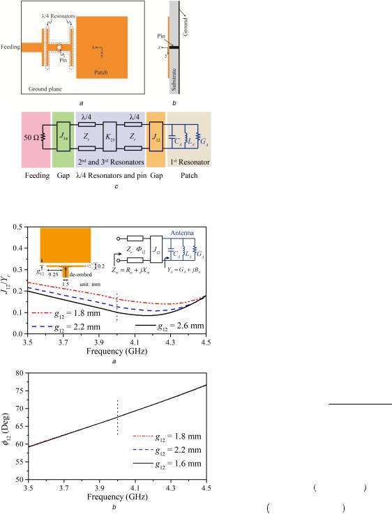
Fig. 1 Physical layout of the proposed FPA and its equivalent circuit
(a) Top view, (b) Side view, (c) Equivalent circuit
Fig. 2 De-embedded J12 inverter parameters of the coupling element between the resonant patch and feeding line under different gap spacings g12
(a) Normalised J12 admittance, (b) Effective electrical length ϕ12 at the feeding side
inspired K inverter are de-embedded to allow one to find their physical dimensions. The relationship between the realisable fractional bandwidth (FBW) and in-band return loss (RL) is further investigated according to the unloaded quality factor of a patch radiator. Finally, a three-order FPA prototype is designed, fabricated, and measured. Measured results agree well with the simulated ones, verifying the effectiveness of the proposed design method.
2 Synthesis of third-order FPA on λ/4 resonators
2.1 Geometry and its equivalent circuit
As depicted in Figs. 1a and b, the proposed FPA consists of a rectangular patch, two H-shaped λ/4 resonators, and a feeding line. The two resonators share a shorting pin at centre and they are stretched into two open-ended stubs with a twice characteristic impedance of their middle portion. The patch and the feeding line are coupled in proximity with these two resonators via parallelcoupled line, while the two resonators are inductively coupled through the shorting pin. In our design, the whole FPA is implemented on a single-layer substrate Rogers 4003C with a thickness of 1.524 mm and a relative permittivity of 3.55.
Fig. 1c depicts its overall equivalent circuit, representing a third-order J–K–J bandpass filter network. Herein, the radiating patch is equivalently represented by a lossy parallel resonator with a radiation-inspired conductance of GA, inductance of LA, and
capacitance of CA near its resonance. The gap in coupled-line
portion between the radiating patch and its adjacent resonator is considered as an equivalent J inverter, so is the same for the gap in coupled-line portion between the first resonator and its adjacent feeding line. Meanwhile, the shorting pin not only provides a shortcircuited terminal to the two λ/4 resonators, but also functions as an equivalent K inverter with inductive coupling.
2.2 De-embedded J–K inverter parameters
Since the J–K inverters are the key coupling parameters in our synthesis design, the coupled-line and via elements will be numerically de-embedded from the full-wave simulation as described below. The physical layout of the parallel-coupled element between the radiating patch and T-shaped line, and its equivalent circuit are depicted in the inset of Fig. 2a. On the basis of the cavity model theorem, the values of GA, LA, and CA can be
calculated with the closed-form formulas in [27, chapter 4] if the patch operates under its TM01 mode. In this paper, the length and
width of the rectangular patch radiator resonating at 4.0 GHz are readily chosen as 18.5 and 25.0 mm, respectively. As such, the values of GA and CA can be calculated as 4.7 mS and 5.5 pF, and
the input impedance (Zin) of the structure in Fig. 2a can be
obtained from full-wave simulation. As indicated in the inset of Fig. 2a, the following equation can be deduced:
YA /J122 + jZr tan ϕ12 |
|
Zin = Zr Zr + jYA /J122 tan ϕ12 |
(1) |
where Zr is the characteristic impedance of the middle line of the
λ/4 resonator, whose value is equal to 80.5 Ω as its strip width is chosen as 1.5 mm. By equating the real and imaginary parts on the left-hand side of (1) to the right-hand side, two simultaneous equations can be derived as
RinZrJ122 − RinBA + XinGA tan ϕ12 = GAZr |
(2a) |
RinGA − XinBA − Zr2J122 tan ϕ12 + XinZrJ122 = ZrBA |
(2b) |
By solving (2a) and (2b), the normalised admittance and effective electrical lengths of J12 inverter can be determined and
they are plotted as a function of frequency in Figs. 2a and b, respectively. From Figs. 2a and b, it can be found that the normalised J12 inverter admittance first goes down and then rises
up as frequency increases. The effective electrical lengths ϕ12are
almost maintained as a constant under three different coupled gap spacings. These results illustrate that the inherent resonant frequency of the λ/4 resonator is hardly changeable as the coupling strength between the patch radiator and its adjacent resonator increases or decreases.
As mentioned above, the shorting pin between the two λ/4 resonators functions as an equivalent K inverter. As analysed in [28, 29], this semi-lumped through-via can be represented as an equivalent circuit in Fig. 3a. On the basis of [29], the normalised impedance and effective electrical lengths of this K23 inverter can
2242 |
IET Microw. Antennas Propag., 2017, Vol. 11 Iss. 15, pp. 2241-2246 |
|
© The Institution of Engineering and Technology 2017 |
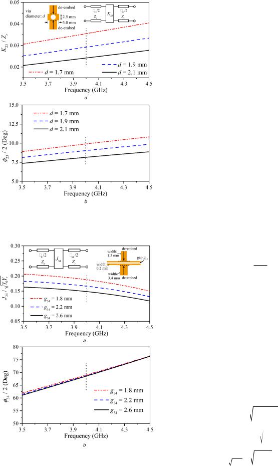
Fig. 3 De-embedded K23 inverter parameters of the via-inspired inductive coupling element under different via diameters d
(a) Normalised K23 inverter impedance, (b) Effective electrical length ϕ23 at two sides
Fig. 4 De-embedded J34 inverter parameters of the coupled-line element under different coupling gap spacings g34
(a) Normalised J34 inverter admittance, (b) Effective electrical length ϕ34 at two sides
be numerically de-embedded from full-wave simulation, and their frequency-dependent results are plotted in Figs. 3a and b, respectively. The effective electrical length varies significantly with respect to via diameter d, thus causing a significant shift in inherent resonant frequency of these two λ/4 resonators. In this situation, the method of extracting the coupling coefficient of two resonators [7, 10, 13, 17] is not suitable herein, since it requires the unchanged resonant frequency of the resonator.
Similarly, the parallel-coupled gap between the first λ/4 resonator and feeding line can be expressed by an equivalent J inverter with effective electrical lines at its two sides. On the basis of [29], the normalised admittance and effective electrical lengths of the J34 inverter can be numerically de-embedded and the
relevant results are plotted in Figs. 4a and b, respectively. From the above analysis and the results in Figs. 2–4, the entire dimensions of the two distinctive coupled gaps and shorting via can be determined to achieve the values of J–K inverters as inquired in the following synthesis design.
2.3 Analysis and synthesis designs
In the following, a synthesis design method will be utilised to obtain the required values of J–K inverters under specified FBW and in-band RL. The equivalent circuit of the proposed FPA is depicted in Fig. 1c and it is analogue to a typical third-order filter network. This filter network will be synthesised herein to achieve the Chebyshev response. First, the normalised Chebyshev low-pass filter prototype with the element values (g0, g1, g2, g3, and g4) is
analysed and synthesised according to the prescribed in-band RL. These element values can be straightforwardly found from a set of design tables in [30, chapter 4], and they become g0 = g4 = 1, g1 =
g3 = 1.225, and g2 = 1.1526 if RL = 13.5 dB is specified.
Since the patch radiator acts as the last resonator in the filter network in Fig. 1c, its unloaded quality factor Qpatch is the same as the external quality factor at its output port. On the basis of the synthesis approach in filter network, the relationship between the Qpatch and other element values can be expressed as
Qpatch = |
g0g1 |
(3) |
FBW |
where FBW stands for the fractional bandwidth.
Since the g0 and g1 are determined by the prescribed in-band
RL, we can figure out from (3) that the FBW and the in-band RL are reversely proportional to each other. When the in-band RL is given, the g0 and g1 can be determined so that the FBW can be
calculated by using (3) for the specified Qpatch. As such, three sets of graphs under different Qpatch are obtained and they are plotted in Fig. 5. As the in-band RL decreases, the FBW gets increment. Under the same in-band RL, the lower the Qpatch, the wider the FBW is. Therefore, this proposed FPA can achieve a wide bandwidth as either the Qpatch or in-band RL is reduced.
In Section 2, as the whole dimensions of the patch radiator are given, its GA and CA are calculated based on the cavity model.
Accordingly, the unloaded quality factor of this patch radiator (Qpatch) can be derived as 29.4 herein. By utilising the filter synthesis approach in [30, chapter 4], the values of J–K inverters in their circuit model in Fig. 1c can be calculated
J12 |
= FBW |
|
πQpatchGA |
(4a) |
|||||
|
4g1g2Yr |
||||||||
Yr |
|
|
|
||||||
K23 = FBWπ |
1 |
|
(4b) |
||||||
g2g3 |
|||||||||
|
Zr |
|
4 |
|
|
||||
|
|
J34 |
= |
|
πFBW |
(4c) |
|||
|
|
YrY0 |
|
4g3g4 |
|||||
where Zr and Yr are the characteristic impedance and admittance of the λ/4 microstrip-line resonator, whose values are found as 80.5 Ω
IET Microw. Antennas Propag., 2017, Vol. 11 Iss. 15, pp. 2241-2246 |
2243 |
© The Institution of Engineering and Technology 2017 |
|

Fig. 5 Relationship between the in-band RL and FBW under different patch unloaded factors Qpatch
Fig. 6 Frequency responses under different in-band RLs and fixed patch unloaded Q factor Qpatch of 29.4
Fig. 7 Comparison in FBW between the proposed FPA and traditional directly fed patch antenna
Fig. 8 Equivalent network of two inductively coupled λ/4 resonators with their three distinctive portions in electrical length
and 1/80.5 S, respectively; Y0 is the port admittance and its value is
0.02 S here.
On the basis of the above analysis, all the values of the circuit model in Fig. 1c can be determined, and the corresponding frequency responses under different in-band RLs and fixed Qpatch = 29.4 are derived as plotted in Fig. 6 for comparison. To achieve RL = 20 dB, three transmission poles are allocated in proximity to each other, thereby forming a relatively narrow bandwidth of
operation with filtering selectivity. If the two poles at the two sides move outwards, the operating bandwidth or FBW progressively becomes wide, whereas the in-band RL tends to be degraded with poor impedance matching. As such, these results exhibit a tradeoff between the FBW and in-band RL if a patch radiator with the fixed Qpatch is formed on a specified dielectric substrate.
Now, let us illustrate the wideband filtering characteristic of the proposed FPA in Fig. 1. Fig. 7 depicts its simulated reflection coefficient with that of a conventional directly fed patch antenna. It is apparent that the proposed third-order FPA achieves the FBW of 4.2% under the selection of RL = 13.5. Compared with the FBW = 1.5% in the latter one, the concerned bandwidth has been increased by 2.8. By virtue of the three in-band poles, the proposed FPA not only widens its bandwidth, but also tremendously sharpens its out- of-band rejection skirt near the lower and upper cut-off frequencies.
In the following, the proposed filtering antenna with the in-band RL of 13.5 dB is designed and implemented as an example. On the basis of (4a)–(4c), the normalised values of J12, K23, and J34 are
calculated as 0.1036, 0.0275, and 0.1634, respectively. Referring to Figs. 2a–4a, the initial values of g12, d, and g34 are chosen as 2.6,
1.9, and 0.4 mm. With the derived g12, d, and g34 and the results in Figs. 2b–4b, the associated effective electrical lengths are: ϕ12 = 67.57°, ϕ23/2 = 9.15°, and ϕ34/2 = 67.73°. Fig. 8 depicts the
equivalent circuit of two inductively coupled λ/4 resonators. It can be understood that the entire electrical length of each λ/4 resonator is composed of three distinctive portions, i.e. its actual electrical length or two dissimilar compensate lengths caused by the coupled line and via elements. To construct these two λ/4 resonators, the electrical compensated lengths (φ1 and φ2) in middle are
determined as 13.28° ( = 90°−ϕ12−ϕ23/2) and 12.12° ( = 90° −ϕ23/2−ϕ34/2), respectively. Note that all the other dimensions have
been given in Figs. 2–4.
On the basis of the above-described procedure, the proposed FPA is designed and simulated. The electric field distribution beneath the patch and the electric current distribution of the whole structure at the centre frequency are plotted in Figs. 9a and b, respectively. As seen from Fig. 9a, the electric field distribution in the x-direction tends to be a sinusoidal function, and the one in the y-direction holds almost constant magnitude. Consequently, the patch antenna is operating in the typical TM10 mode. In Fig. 9b, the
electric current density is mainly concentrated around the central line of the patch along the y-direction, contributing to the broadside radiation.
In this work, the resonators and antenna are placed on the same substrate, but other feeding topology may also be practicable. For example, the feeding circuits and the antenna are separately formed in the top and bottom interfaces of a two-layered substrate with a ground plane in its middle interface. Herein, the coupling between them is modelled as the J inverter, which can be extracted with resorting to the proposed method above. In this case, synthesis design of this kind of filtering antenna structure can be similarly executed as reported in this work.
3 Measured results and verification
Next, the FPA is fabricated and measured to verify the effectiveness of the proposed design. Fig. 10 shows the photograph of the fabricated FPA with the detailed dimensions. In this work, frequency responses of its reflection coefficient and radiation gain are measured with the use of the Roger Schwarz ZNB-20 vector network analyser and SATIMO near-field antenna measurement system, respectively. The simulated and measured frequency responses of reflection coefficients and gains are plotted in Fig. 11. They are found in good agreement with each other, thus confirming the predicted wideband and high-selective performances of the proposed FPA. More specifically, the measured reflection coefficient is below −13.0 dB in the whole operating band, over which three resonant poles are produced at 3.85, 3.97, and 4.08 GHz. Plus these three in-band poles, the proposed FPA not only holds a wide operating band, but also achieves the third-order bandpass filtering selectivity for both of reflection coefficient and
2244 |
IET Microw. Antennas Propag., 2017, Vol. 11 Iss. 15, pp. 2241-2246 |
|
© The Institution of Engineering and Technology 2017 |

Fig. 9 Electric field distribution and electric current distribution at the centre frequency (4.0 GHz)
(a) Electric field distribution beneath the patch, (b) Electric current distribution of the whole structure
Fig. 10 Photograph of the fabricated third-order FPA with all the dimensions to be denoted
radiation gain as illustrated in Fig. 11. Herein, the radiation gains attain an approximately flat response around the central frequency in simulation and measurement. There is a peak of 4.85 dBi in the measured gain response, and the realised gain decreases rapidly as the frequency is below 3.8 GHz and above 4.1 GHz, thereby exhibiting the highly sharpened skirt selectivity.
Fig. 12 depicts the simulated and measured radiation patterns of the designed FPA in the E and H planes at 3.9, 4.0, and 4.1 GHz. It is observed herein that the main radiation direction is maintained in the broadside direction regardless of varied frequencies. The 3 dB beamwidths in the E-plane at 3.9, 4.0, and 4.1 GHz are found to be 81.5°, 81.0°, and 90.2°, respectively, and those in the H-plane to be 74.0°, 85.5°, and 74.0°, respectively. These results in radiation patterns have shown reasonably stable radiation characteristic over a wide operating band.
Fig. 11 Simulated and measured reflection coefficients and radiation gain of the implemented FPA in a frequency range of 3.5–4.5 GHz
Fig. 12 Simulated and measured radiation patterns of the proposed FPA in the E and H planes at the three different frequencies
(a) 3.9 GHz, (b) 4.0 GHz, (c) 4.1 GHz
4 Conclusion
This paper presents a compact FPA based on a filtering topology including two λ/4 resonators. In analogue to an equivalent thirdorder filter network, the proposed FPA can produce three in-band transmission poles from the two λ/4 resonators and the radiating patch resonator. These poles allow us to effectively widen its operating bandwidth and sharpen its out-of-band rejection skirt. Since the λ/4 resonator only occupies half a length of the λ/2 resonator, the proposed FPA has the miniaturised size, especially as
IET Microw. Antennas Propag., 2017, Vol. 11 Iss. 15, pp. 2241-2246 |
2245 |
© The Institution of Engineering and Technology 2017 |
|
the high-order filtering topology needs to be implemented toward enhanced filtering selectivity. In our design, its equivalent circuit network with J–K inverters is applied to synthesise its frequency response under the Chebyshev function. At last, a prototype FPA at 4.0 GHz is designed, fabricated, and measured. The simulated and measured results agree well with each other, providing good verification for the proposed design method.
5 Acknowledgments
This work was supported by the National Natural Science Foundation of China under General Program Grant (61571468), University of Macau under Multi-Year Research Grant (MYRG2015-00010-FST), and the Macao Science and Technology Development Fund under FDCT Research Grant (051/2014/A1).
6 References
[1]Mandal, M.K., Chen, Z.N.: ‘Compact wideband coplanar stripline bandpass filter with wide upper stopband and its application to antennas’, IET Microw. Antennas Propag., 2010, 4, (12), pp. 2166–2171
[2]Nova, O.A., Bohorquez, J.C., Pena, N.M., et al.: ‘Filter-antenna module using substrate integrated waveguide cavities’, IEEE Antennas Wirel. Propag. Lett., 2011, 10, pp. 59–62
[3]Yusuf, Y., Cheng, H.T., Gong, X.: ‘Co-designed substrate-integrated waveguide filters with patch antennas’, IET Microw. Antennas Propag., 2013, 7, (7), pp. 493–501
[4]Cheng, H.T., Yusuf, Y., Gong, X.: ‘Vertically integrated three-pole filter/ antennas for array applications’, IEEE Antennas Wirel. Propag. Lett., 2011, 10, pp. 278–281
[5]Nadan, T.E., Coupez, J.P., Toutain, S., et al.: ‘Integration of an antenna/filter device, using a multi-layer, multi-technology process’. Proc. 28th European Microwave Conf., Amsterdam, Netherlands, March 2007, pp. 672–677
[6]Zuo, J.H., Chen, X.W., Han, G.R., et al.: ‘An integrated approach to RF antenna-filter co-design’, IEEE Antennas Wirel. Propag. Lett., 2009, 8, pp. 141–144
[7]Jiang, Z.H., Werner, D.H.: ‘A compact, wideband circularly polarized codesigned filtering antenna and its application for wearable devices with low SAR’, IEEE Trans. Antennas Propag., 2015, 63, (9), pp. 3808–3818
[8]Tamijani, A.A., Rizk, J., Rebeiz, G.: ‘Integration of filters and microstrip antennas’. Proc. IEEE AP-S Int. Symp. Digest, San Antonio, USA, August 2002, pp. 874–877
[9]Chuang, C.T., Chung, S.J.: ‘Synthesis and design of a new printed filtering antenna’, IEEE Trans. Antennas Propag., 2011, 59, (3), pp. 1036–1042
[10]Mansour, G., Lancaster, M.J., Hall, P.S., et al.: ‘Design of filtering microstrip antenna using filter synthesis approach’, Prog. Electromagn. Res., 2014, 145, pp. 59–67
[11]Lin, C.K., Chung, S.J.: ‘A compact filtering microstrip antenna with quasielliptic broadside antenna gain response’, IEEE Antennas Wirel. Propag. Lett., 2011, 10, pp. 381–384
[12]Chen, X.W., Zhao, F.X., Yan, L.Y., et al.: ‘A compact filtering antenna with flat gain response within the passband’, IEEE Antennas Wirel. Propag. Lett., 2013, 12, pp. 857–860
[13]Wu, W.J., Yin, Y.Z., Zuo, S.L., et al.: ‘A new compact filter-antenna for modern wireless communication systems’, IEEE Antennas Wirel. Propag. Lett., 2011, 10, pp. 1131–1134
[14]Tang, M.C., Chen, Y., Ziolkowski, R.W.: ‘Experimentally validated, planar, wideband, electrically small, monopole filtennas based on capacitively loaded loop resonators’, IEEE Trans. Antennas Propag., 2016, 64, (8), pp. 3353– 3360
[15]Mao, C.X., Gao, S., Wang, Y., et al.: ‘Multimode resonator-fed dual-polarized antenna array with enhanced bandwidth and selectivity’, IEEE Trans. Antennas Propag., 2015, 63, (12), pp. 5492–5499
[16]Lin, C.K., Chung, S.J.: ‘A filtering microstrip antenna array’, IEEE Trans. Microw. Theory Tech., 2011, 59, (11), pp. 2856–2863
[17]Chen, F.C., Hu, H.T., Li, R.S., et al.: ‘Design of filtering microstrip antenna array with reduced sidelobe level’, IEEE Trans. Antennas Propag., 2017, 65, (2), pp. 903–908
[18]Mao, C.X., Gao, S., Wang, Y., et al.: ‘An integrated filtering antenna array with high selectivity and harmonics suppression’, IEEE Trans. Microw. Theory Tech., 2016, 64, (6), pp. 1798–1805
[19]Nadaud, K., Tong, D.L.H., Fourn, E.: ‘Filtering slot antenna using coupled line resonator’. Proc. Ninth European Microwave Integrated Circuit Conf., Rome, Italy, December 2014, pp. 556–559
[20]Chuang, C.T., Chung, S.J.: ‘A compact printed filtering antenna using a ground-intruded coupled line resonator’, IEEE Trans. Antennas Propag., 2011, 59, (10), pp. 3630–3637
[21]Zhang, X.Y., Duan, W., Pan, Y.M.: ‘High-gain filtering patch antenna without extra circuit’, IEEE Trans. Antennas Propag., 2015, 63, (12), pp. 5883–5888
[22]Pan, Y.M., Hu, P.F., Zhang, X.Y., et al.: ‘A low-profile high-gain and wideband filtering antenna with metasurface’, IEEE Trans. Antennas Propag., 2016, 64, (5), pp. 2010–2016
[23]Zhang, Y., Zhang, X.Y., Ye, L.H., et al.: ‘Dual-band base station array using filtering antenna elements for mutual coupling suppression’, IEEE Trans. Antennas Propag., 2016, 64, (8), pp. 3423–3430
[24]Lim, E.H., Leung, K.W.: ‘Use of the dielectric resonator antenna as a filter element’, IEEE Trans. Antennas Propag., 2008, 56, (1), pp. 5–10
[25]Luo, G.Q., Hong, W., Tang, H.J., et al.: ‘Filtenna consisting of horn antenna and substrate integrated waveguide cavity FSS’, IEEE Trans. Antennas Propag., 2007, 55, (1), pp. 92–98
[26]Zhang, J.D., Zhu, L., Wu, Q.S., et al.: ‘A compact microstrip-fed patch antenna with enhanced bandwidth and harmonic suppression’, IEEE Trans. Antennas Propag., 2016, 64, (12), pp. 5030–5037
[27]Garg, R., Bhartia, P., Bahl, I., et al.: ‘Microstrip antenna design handbook’
(Artech House, Norwood, 2001)
[28]Zhu, L., Wu, K.: ‘Accurate circuit model of interdigital capacitor and its application to design of new quasi-lumped miniaturized filters with suppression of harmonic resonance’, IEEE Trans. Microw. Theory Tech., 2000, 48, (3), pp. 347–356
[29]Zhang, S.B., Zhu, L.: ‘Synthesis method for even-order symmetrical Chebyshev bandpass filters with alternative J/K inverters and λ/4 resonators’,
IEEE Trans. Microw. Theory Tech., 2013, 61, (2), pp. 808–816
[30]Matthaei, G.L., Young, L., Jones, E.M.T.: ‘Microwave filters, impedancematching networks and coupling structures’ (Artech House, Norwood, MA, 1980)
2246 |
IET Microw. Antennas Propag., 2017, Vol. 11 Iss. 15, pp. 2241-2246 |
|
© The Institution of Engineering and Technology 2017 |