

диафрагмированные волноводные фильтры / 82750c9d-ae84-491b-a6e9-df0f0bc14cab
.pdf1408 |
IEEE TRANSACTIONS ON COMPONENTS, PACKAGING AND MANUFACTURING TECHNOLOGY, VOL. 6, NO. 9, SEPTEMBER 2016 |
Integration Design of Filtering Antenna With
Load-Insensitive Multilayer Balun Filter
Hui Tang, Jian-Xin Chen, Member, IEEE, Hui Chu, Guo-Qing Zhang, Yong-Jie Yang, and Zhi-Hua Bao
Abstract— Integration design of a filtering antenna fed by a load-insensitive multimode balun bandpass filter is proposed in this paper. The balun filter is designed and realized using multilayer structure for miniaturization. To be directly integrated into the antenna, both amplitude and phase performances of the balun filter are investigated with different complex load impedances. With insensitive responses against the load, this balun filter is utilized to design a filtering antenna as the feeding of a quasi-Yagi antenna, which is considered as a frequency-dependent differential complex load. The radiation characteristics are improved by applying a metallic shield as the package for the proposed design. To verify the design concept, an experimental filtering antenna is designed, fabricated, and measured with almost the same passband as that of the balun filter benefiting from the load-insensitive property of the latter. The simulated and measured results are presented, showing good agreement.
Index Terms— Balun filter, filtering antenna, integration design, load-insensitive, quasi-Yagi antenna.
I. INTRODUCTION
WITH the development of modern wireless and mobile communication systems, radio frequency front ends are highly required with enhanced performance in convenience,
stability, low cost, and compact size. Minimizing the size of antenna is one of the solutions and has attracted wide attention [1]. Multifunction components are also welcomed in a system for enhancing the overall performance and reducing circuit area, such as balun filters with the function of both filtering and balance-to-unbalance conversion [2]–[8]. Integration design is another effective measure with an ability to provide low impedance matching complexity, low power consumption, and low-cost solution for microwave systems [7]–[17]. In many communication and radar systems, filters, baluns, and antennas are critical components and usually needed simultaneously. Filters are utilized to suppress unexpected out-of-band signals. In the feeding networks of dipole
Manuscript received January 21, 2016; revised May 8, 2016; accepted August 8, 2016. Date of publication August 31, 2016; date of current version September 20, 2016. This work was supported in part by the National Natural Science Foundation of China under Grant 61501265, Grant 61301044, and Grant 61271136, the National Natural Science Foundation of Jiangsu under Grant BK20161281, the Graduate Research & Innovation Plan Project of Jiangsu Province and Nantong University under Grant KYLX15_1314 and Grant YKC15001, and the Science-Technology Programs of Nantong under Grant CP22014005 and Grant AA2014013. Recommended for publication by Associate Editor T.-L. Wu upon evaluation of reviewers’ comments.
The authors are with the School of Electronics and Information, Nantong University, Nantong 226019, China (e-mail: jjxchen@hotmail.com).
Color versions of one or more of the figures in this paper are available online at http://ieeexplore.ieee.org.
Digital Object Identifier 10.1109/TCPMT.2016.2600541
antennas [6]–[8], [18] or other differential antennas [19], baluns are usually required to transfer unbalanced single-ended signals into balanced or differential ones. In the traditional way, each component is designed individually with standard 50ports and then assembled into a system, leading to large size, high complexity, or detuning with large loss. However, integration design realizes that multiple elements cooperate in an entity and the 50transitions between the separate structures are not required, resulting in compact and highefficient systems. The integration of an antenna and a balun is the focus of many researchers [8]–[10]. Lots of efforts have also been paid in the integration of an antenna and a filter [11]–[17]. Integrated antennas with balun filters are also studied popularly [6]–[8]. In most cases, a balun or a filter is composed of resonators with the same resonant frequency as that of the antenna. It brings interferences on the return loss and the antenna gain, especially at the band edges. As a result, the passband and gain of the integrated antenna generally deteriorate. Designing filtering antennas is one of the possible solutions in which the radiation elements act in selecting signals without mutual interferences [12]–[17]. A four-element filtering antenna array with each element having filtering function and the feeding network consisting of one power divider and two baluns is presented in [18]. Using loadinsensitive baluns or filters to integrate into antennas is another good solution. It is similar to an insensitive bandpass filter with acceptable responses under different load impedances, which is applied in a high-efficiency power amplifier [21]. Loadinsensitive active components can count antenna impedance mismatch caused by frequency variation and environmental effects as well [22]. A load-insensitive balun or filter allows its load to be an impedance-varying antenna, without evident response changes. The impedance mismatching in some degree between an antenna and the balun or filter would not significantly impact the performances of the system. Therefore, load insensitivity of microwave devices can provide extensive application and easy design procedure.
In this paper, the integration design of a filtering antenna fed by a load-insensitive multimode balun filter is proposed, as shown in Fig. 1. It consists of a load-insensitive multimode balun filter, a quasi-Yagi antenna, and connecting lines. A pair of back-to-back coupled patches is utilized to design the balun filter using multilayer circuit technology. The amplitude and phase performances of the balun filter are investigated, showing good insensitivity against the complex load impedance. In the integration design, the balun filter is combined with the antenna through essential connecting lines.
2156-3950 © 2016 IEEE. Personal use is permitted, but republication/redistribution requires IEEE permission. See http://www.ieee.org/publications_standards/publications/rights/index.html for more information.
TANG et al.: INTEGRATION DESIGN OF FILTERING ANTENNA WITH LOAD-INSENSITIVE MULTILAYER BALUN FILTER |
1409 |
|||||||||||||||||||||||||||
|
|
|
|
|
|
|
|
|
|
|
|
|
|
|
|
|
|
|
|
|
|
|
|
|
|
|
|
|
|
|
|
|
|
|
|
|
|
|
|
|
|
|
|
|
|
|
|
|
|
|
|
|
|
|
|
|
|
|
|
|
|
|
|
|
|
|
|
|
|
|
|
|
|
|
|
|
|
|
|
|
|
|
|
|
|
|
|
|
|
|
|
|
|
|
|
|
|
|
|
|
|
|
|
|
|
|
|
|
|
|
|
|
|
|
|
|
|
|
|
|
|
|
|
|
|
|
|
|
|
|
|
|
|
|
|
|
|
|
|
|
|
|
|
|
|
|
|
|
|
|
|
|
|
|
|
|
|
|
|
|
|
|
|
|
|
|
|
|
|
|
|
|
|
|
|
|
|
|
|
|
|
|
|
|
|
|
|
|
|
|
|
|
|
|
|
|
|
|
|
|
|
|
|
|
|
|
|
|
|
|
|
|
|
|
|
|
|
|
|
|
|
|
|
|
|
|
|
|
|
|
|
|
|
|
|
|
|
|
|
|
|
|
|
|
|
|
|
|
|
|
|
|
|
|
|
|
|
|
|
|
|
|
|
|
|
|
|
|
|
|
|
|
|
|
|
|
|
|
|
|
|
|
|
|
|
|
|
|
|
|
|
|
|
|
|
|
|
|
|
|
|
|
|
|
|
|
|
|
|
|
|
|
|
|
|
|
|
|
|
|
|
|
|
|
|
|
|
|
|
|
|
|
|
|
|
|
|
|
|
|
|
|
|
|
|
|
|
|
|
|
|
|
|
|
|
|
|
|
|
|
|
|
|
|
|
|
|
|
|
|
|
|
|
|
|
|
|
|
|
|
|
|
|
|
|
|
|
|
|
|
|
|
|
|
|
|
|
|
|
|
|
|
|
|
|
Fig. 1. 3-D view of the proposed quasi-Yagi antenna integrated with load-insensitive multilayer balun filter.
The connecting lines are not λ/4 impedance transformers or standard transmission lines with 50characteristic impedance. They act as an optimizer in the proposed design. A metallic shield is used as a package for the filtering antenna, and brings improved radiation performance. The implemented filtering antenna shows not only a good bandpass response with almost the same bandwidth as that of the balun filter, but also well-defined reflection coefficient, desired gain, low cross-polarization level, and stable copolarization radiation characteristic throughout the passband.
Fig. 2. Layout of the proposed balun filter. (a) Bottom layer.
(b) Middle layer. (c) Top layer. (d) Side view.
II. LOAD-INSENSITIVE MULTILAYER MULTIMODE
BANDPASS BALUN FILTER
In order to achieve both bandpass characteristic and balun performance in a multimode configuration, patch resonators are chosen in the design. A patch resonator can provide dual modes, low insertion loss, and high power-handling capability [23]. Multilayer structure is an effective solution to couple dual-mode patch resonators [5] and to minimize the circuit size. Lots of technologies can realize multilayer circuits, such as multilayer printed circuit board (PCB) [24] and low-temperature cofired ceramic [25]. In multilayer PCB technology, the prepreg is softened by heat and pressure and solidifies after cooling to glue layers. Due to its low cost and convenience, multilayer PCB is utilized in this design.
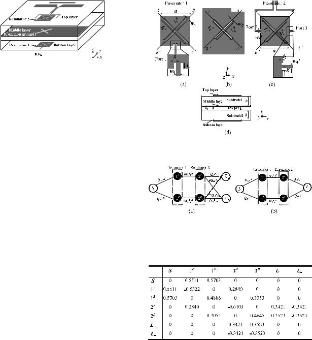
The layout of the multimode balun filter in this section is presented in Fig. 2. Two slotted patches (noted as Resonator 1 and 2, respectively) placed back to back in different layers and sharing the slotted common ground provide a quad-mode structure. Here, Port 1 is the single-ended input port. With 180◦ phase difference, Ports 2 and 3 constitute the differential output ports. Though the flowing paths of electric current on the slotted patch are rerouted and electrically stretched, the electrical length of each flowing path between the two opposite sides is still half-wavelength at the corresponding resonant frequency. Therefore, the cross-slotted patch resonator naturally offers Ports 2 and 3 with 180° phase difference. The rerouted level of the flowing paths of electric current densities depends on the lengths of the slots etched on the patches [4], [5], [23]. The resonant frequencies of the four modes 1A , 1B , 2A , and 2B can be controlled through changing the lengths l1A , l1B , l2A , and l2B in Fig. 2, respectively. The modes (1A/2A ) along A A are orthogonal to those (1B /2B ) along B B . The coupling paths of the modes are supplied and controlled by the slots etched on the common ground with the lengths of lgA and lgB . This property is also used in [5], but it presented
Fig. 3. Coupling schemes of (a) proposed multimode balun filter and (b) corresponding single-ended fourth-order bandpass filter.
TABLE I
COUPLING MATRIX FOR THE MULTIMODE BALUN FILTER
a balun filter synthesized from a dual-band filter, with dual passbands and the standard 50- I/O port impedances.
The coupling scheme of the proposed balun filter is shown in Fig. 3(a), which is extended from a corresponding singleended fourth-order bandpass filter with coupling scheme shown in Fig. 3(b). The path S-1A -2A -L is for the modes along diagonal line A A , and the path S-1B -2B -L is for those along B B . Thus, all the lengths of the slots can be properly adjusted to achieve a multimode balun filter.
To realize a multimode 3-dB passband from 1.57 to 1.88 GHz, the coupling matrix for the proposed balun filter is synthesized from its corresponding single-ended fourth-order bandpass filter, as shown in Table I. The external Q-factors of the balun filter and the corresponding bandpass filter for the

1410 |
IEEE TRANSACTIONS ON COMPONENTS, PACKAGING AND MANUFACTURING TECHNOLOGY, VOL. 6, NO. 9, SEPTEMBER 2016 |
|||||||||||
extension can be expressed as follows: |
|
|
|
|
|
|
|
|
|
|||
|
|
|
|
|
|
|
|
|
||||
QeS1N = |
1 |
|
|
|
|
|
(1) |
|
|
|
|
|
|
|
|
|
|
|
|
|
|
|
|||
FBW × MS21N |
|
|
|
|
|
|||||||
Qe2N L = |
1 |
|
|
|
|
|
(2) |
|
|
|
|
|
FBW × M22N L |
|
√ |
|
|
|
|
|
|
|
|||
|
|
|
|
|
|
|
|
|
|
|||
M2N L+ = −M2N L− = M2N L / |
2 |
|
(3) |
|
|
|
|
|
||||
Qe2N L = Qe2N L+/2 = Qe2N L−/2. |
(4) |
|
|
|
|
|
||||||
Here, N = A or B. FBW, M2N L , and QeSN 1 are the fractional bandwidth, normalized coupling coefficients, and external Q-factor of input port, respectively. Qe2NL is the output port external Q-factor of the corresponding single-ended bandpass filter. Qe2NL+ and Qe2NL− are the output port external Q-factors of the balun filter.
The resonator frequencies of the modes can be calculated by the diagonal elements in the coupling matrix [26]. The
relationship is |
|
|
|
|
|
|
|||
Mii |
= |
f 2 |
− |
f 2 /( f |
× |
fi ) |
(i |
= |
1A , 2A , 1B , or 2B ) |
|
0 |
i |
|
|
|
||||
where f0, fi , and f are the center frequency, the resonant frequency of the according mode, and the bandwidth, respectively. The lengths l1A , l2A , l1B , and l2B of the slots etched on the patches are determined by the resonant frequencies calculated according to (5). The coupling coefficient Ki j between the i th and j th modes can be extracted by the following equation [27]:
Ki j |
= |
K j i |
= |
f 2 |
− |
f 2 / f 2 |
+ |
f 2 |
|
|
2 |
1 2 |
1 |
||||
|
= FBW × Mi j |
(i = 1A , j = 2A or i = 1B , j = 2B ). |
||||||
|
|
|
|
|
|
|
|
(6) |
Here, f1 and f2 represent the lower and higher resonant frequencies for the two coupled modes, respectively. The lengths lgA and lgB of the slots etched on the common ground are decided by the coupling coefficients K 1A 2A and K 1B 2B between the coupled modes. The external Q-factors can be extracted and attained by
Qe = fq0/ f±90°. |
(7) |
fq0 and f±90° denote the central frequency of the I/O couplings and the ±90° bandwidth with respect to the absolute phase at fq0, respectively. The lengths i1 and i2 of the gaps at the I/O ports depend on the according external Q-factors.
A multimode balun filter based on the multilayer structure is designed using two Rogers4003C substrates and one layer of prepreg, with the dielectric constant εr = 3.38, loss tangent of 0.0027, the thickness of each substrate h = 0.508 mm, and the thickness of prepreg h1 = 0.1 mm. The dimension w0 = 1.5 mm is the width of 50microstrip as the feeding line of the input port, Port 1. According to (5)–(7), the extracted values against the corresponding dimensions are investigated and depicted in Fig. 4. The relationship between Qe2NL and Qe2NL+/Qe2NL− satisfies (4). Compared to the coupling matrix in Table I, the design parameters of the balun filter can be obtained and then optimized. The specific dimensions of the circuit are adopted as shown in Table II.
Fig. 4. Coupling coefficients and external Q-factors with different according dimensions. (a) K 1A 2A . (b) K 1B 2B . (c) QeAS1 and QeBS1. (d) Qe2AL
TABLE II
DESIGN PARAMETERS FOR THE MULTIMODE BALUN FILTER IN FIG. 2
To be directly integrated into an antenna without impedance transformer, the most challenging performance of the balun filter is the insensitivity with different load impedances. Because
of the symmetry of the differential output ports, |
we add |
the two same loads with complex impedance Z L |
to them. |
Fig. 5(a)–(c) displays the EM simulated responses of the balun filter with a variable complex load impedance Z L and a fixed single-ended input impedance of 50 . The parameters of the balun filter with different complex loads are listed in Table III. The results are simulated using Ansoft HFSS and Agilent Advanced Design System. They show that the balun filter exhibits acceptable in-band performance of |S11| < −11 dB, the amplitude imbalance less than 0.83 dB, and phase difference within 180° ± 2° in the range of Re(Z L ) from 30 to 75 with Im(Z L ) = 0 and in the range of Im(Z L ) from −20 to +20 with Re(Z L ) = 50 .
When the load impedances are pure resistances and increase from 30 to 75 in Fig. 5(a), the in-band insertion losses slightly change with both |S21| and |S31| keeping within 3 ± 0.5 dB and amplitude imbalance (|S21| − |S31|) keeping within ±0.44 dB. However, the maximum in-band return loss |S11| changes a little greater from −15.10 to −11.04 dB, and it can be seen that |S11| is optimal when Z L = 50 . Considering complex impedance loads in Fig. 5(b), when Re(Z L ) keeps fixed at 50 and Im(Z L ) varies from −20 to +20 , the in-band insertion losses change a little more

TANG et al.: INTEGRATION DESIGN OF FILTERING ANTENNA WITH LOAD-INSENSITIVE MULTILAYER BALUN FILTER |
1411 |
||||||||||||||||||||||||||||
|
|
|
|
|
|
|
|
|
|
|
|
|
|
|
|
|
|
|
|
|
|
|
|
|
|
|
|
|
|
|
|
|
|
|
|
|
|
|
|
|
|
|
|
|
|
|
|
|
|
|
|
|
|
|
|
|
|
|
|
|
|
|
|
|
|
|
|
|
|
|
|
|
|
|
|
|
|
|
|
|
|
|
|
|
|
|
|
|
|
|
|
|
|
|
|
|
|
|
|
|
|
|
|
|
|
|
|
|
|
|
|
|
|
|
|
|
|
|
|
|
|
|
|
|
|
|
|
|
|
|
|
|
|
|
|
|
|
|
|
|
|
|
|
|
|
|
|
|
|
|
|
|
|
|
|
|
|
|
|
|
|
|
|
|
|
|
|
|
|
|
|
|
|
|
|
|
|
|
|
|
|
|
|
|
|
|
|
|
|
|
|
|
|
|
|
|
|
|
|
|
|
|
|
|
|
|
|
|
|
|
|
|
|
|
|
|
|
|
|
|
|
|
|
|
|
|
|
|
|
|
|
|
|
|
|
|
|
|
|
|
|
|
|
|
|
|
|
|
|
|
|
|
|
|
|
|
|
|
|
|
|
|
|
|
|
|
|
|
|
|
|
|
|
|
|
|
|
|
|
|
|
|
|
|
|
|
|
|
|
|
|
|
|
|
|
|
|
|
|
|
|
|
|
|
|
|
|
|
|
|
|
|
|
|
|
|
|
|
|
|
|
|
|
|
|
|
|
|
|
|
|
|
|
|
|
|
|
|
|
|
|
|
|
|
|
|
|
|
|
|
|
|
|
|
|
|
|
|
|
|
|
|
|
|
|
|
|
|
|
|
|
|
|
|
|
|
|
|
|
|
|
|
|
|
|
|
|
|
|
|
|
|
|
|
|
|
|
|
|
|
|
|
|
|
|
|
|
|
|
|
|
|
|
|
|
|
|
|
|
|
|
|
|
|
|
|
|
|
|
|
|
|
|
|
|
|
|
|
|
|
|
|
|
|
|
|
|
|
|
|
|
|
|
|
|
|
|
|
|
|
|
|
|
|
|
|
|
|
|
|
|
|
|
|
|
|
|
|
|
|
|
|
|
|
|
|
|
|
|
|
|
|
|
|
|
|
|
|
|
|
|
|
|
|
|
|
|
|
|
|
|
|
|
|
|
|
|
|
|
|
|
|
|
|
|
|
|
|
|
|
|
|
|
|
|
|
|
|
|
Fig. 5. Balun filter responses with different differential load impedances and 50single input impedance. (a) Magnitudes of S-parameters with different load resistances. (b) Magnitudes of S-parameters with different load reactances. (c) Phase differences.
TABLE III
IN-BAND PARAMETERS OF THE LOAD-INSENSITIVE MULTIMODE
BALUN FILTER WITH DIFFERENT LOAD IMPEDANCES
AT THE DIFFERENTIAL OUTPUT PORTS
significantly with |S21| decreasing and |S31| increasing. In the mentioned load range, Z L = (50 − j 20) brings the in-band amplitude imbalance with Max (||S21| − |S31||) = 0.83 dB and the largest in-band return loss of −11.5 dB in the high-
frequency part of the passband. While the capacitive reactance gradually changes into inductive, the amplitude imbalance first reduces and arrives at the minimum when Im (Z L ) = 0. Then,
it increases when the inductive reactance increases. When Z L = (50+ j 20) , Max (||S21|−|S31||) = 0.79 dB. However, the larger the inductive reactance, the larger the in-band return
loss near the low-frequency edge of the passband. For in-band phase difference in the passband shown in Fig. 5(c), it increases when Z L is a pure resistance and increases. With a fixed resistance of 50 , when the reactance of Z L gets closer to zero, the phase difference decreases. The change of the phase difference against complex load impedance throughout the passband is less than 1° in the mentioned load range. At the same time, the bandwidth of the balun filter remains about 17% with variation less than 1.5% against complex output impedances Z L in the mentioned load range. It is obvious that the multimode balun filter displays insensitivity against its complex output load impedances within the certain range.
For demonstration, a prototype of the balun filter with standard 50port impedances is fabricated. The dimension

1412 |
|
|
|
|
|
|
|
|
|
|
|
|
IEEE TRANSACTIONS ON COMPONENTS, PACKAGING AND MANUFACTURING TECHNOLOGY, VOL. 6, NO. 9, SEPTEMBER 2016 |
||||||||||||||||||
|
|
|
|
|
|
|
|
|
|
|
|
|
|
|
|
|
|
|
|
|
|
|
|
|
|
|
|
|
|
|
|
|
|
|
|
|
|
|
|
|
|
|
|
|
|
|
|
|
|
|
|
|
|
|
|
|
|
|
|
|
|
|
|
|
|
|
|
|
|
|
|
|
|
|
|
|
|
|
|
|
|
|
|
|
|
|
|
|
|
|
|
|
|
|
|
|
|
|
|
|
|
|
|
|
|
|
|
|
|
|
|
|
|
|
|
|
|
|
|
|
|
|
|
|
|
|
|
|
|
|
|
|
|
|
|
|
|
|
|
|
|
|
|
|
|
|
|
|
|
|
|
|
|
|
|
|
|
|
|
|
|
|
|
|
|
|
|
|
|
|
|
|
|
|
|
|
|
|
|
|
|
|
|
|
|
|
|
|
|
|
|
|
|
|
|
|
|
|
|
|
|
|
|
|
|
|
|
|
|
|
|
|
|
|
|
|
|
|
|
|
|
|
|
|
|
|
|
|
|
|
|
|
|
|
|
|
|
|
|
|
|
|
|
|
|
|
|
|
|
|
|
|
|
|
|
|
|
|
|
|
|
|
|
|
|
|
|
|
|
|
|
|
|
|
|
|
|
|
|
|
|
|
|
|
|
|
|
|
|
|
|
|
|
|
|
|
|
|
|
|
|
|
|
|
|
|
|
|
|
|
|
|
|
|
|
|
|
|
|
|
|
|
|
|
|
|
|
|
|
|
|
|
|
|
|
|
|
|
|
|
|
|
|
|
|
|
|
|
|
|
|
|
|
|
|
|
|
|
|
|
|
|
|
|
|
|
|
|
|
|
|
|
|
|
|
|
|
|
|
|
|
|
|
|
|
|
|
|
|
|
|
|
|
|
|
|
|
|
|
|
|
|
|
|
|
|
|
|
|
|
|
|
|
|
|
|
|
|
|
|
|
|
|
|
|
|
|
|
|
|
|
|
|
|
|
|
|
|
|
|
|
|
|
|
|
|
|
|
|
|
|
|
|
|
|
|
|
|
|
|
|
|
|
|
|
|
|
|
|
|
|
|
|
|
|
|
|
|
|
|
|
|
|
|
|
|
|
|
|
|
|
|
|
|
|
|
|
|
|
|
|
|
|
|
|
|
|
|
|
|
|
Fig. 6. Simulated and measured S-parameters of the proposed balun filter.
(a) Magnitudes of S-parameters. (b) Phase differences.
w0 = 1.24 mm in Fig. 2 is the width of 50microstrip line as the feeding lines of Ports 2 and 3. Fig. 6(a) displays the ideal amplitude-frequency response according to the coupling matrix in Table I, the simulated results from Ansoft HFSS, and the measured results carried out by Agilent N5230C vector network analyzer. Simulated and measured phase differences are displayed in Fig. 6(b). The measured results show a 3-dB passband of 17% (from 1.575 to 1.865 GHz) with a slight shift from the simulated one due to the tolerance in fabrication process. The measured in-band maximum insertion loss and the return loss of the proposed multimode balun filter are (3 + 1.4) and 19.6 dB. The measured maximum amplitude imbalance and phase difference between the two differential ports are, respectively, within ±0.3 dB and 180° ± 3° in the whole passband.
The load range of Z L discussed in this section is for a three-port balun network. For differentially driven loads, the input impedances are given in differential definition. To unify the expression, we derive the relationship between the differential load impedance and the load impedances of the threeport network. For the output ports in the three-port network, I2 and I3, representing the currents of Ports 2 and 3, follow as:
I2 = −I3 = I. |
(8) |
The differential load impedance at the differential port of the balun filter noted as Zd L can be described using two loads added to the two output ports, respectively, noted as Z2L and Z3L , as follows:
Z |
|
= |
|
Vd L |
|
I2 Z2L − I3 Z3L |
|
|
2VL |
|
2Z |
|
(9) |
d L |
|
I |
= |
I |
= |
|
I |
= |
L |
||||
|
|
|
|
|
|||||||||
where Z2L |
|
= |
Z3L |
= Z L . Thus, |
for |
highly |
|
required |
|||||
performances |
|
of |
the |
balun filter, |
we |
|
accordingly expect |
||||||
60 < Re(Zd L ) < 150 and −40 < Im(Zd L ) < 40 in the passband.
III. INTEGRATION DESIGN OF FILTERING ANTENNA
As discussed in Section II, the balun shows good insensitivity against its complex output load impedances. It means that the balun filter is suitable to be integrated to other components that do not necessarily have 50single or 100differential input impedance. Remarkably, the feature of insensitivity enables the circuit to counter the frequency variation of loaded impedances.
Fig. 7. Top view of the proposed filtering antenna.
TABLE IV
DESIGN PARAMETERS FOR THE QUASI-YAGI ANTENNA IN FIG. 7
In the proposed integration design, the input impedance of the antenna is a frequency variant quantity. Thus, it can be regarded as a varying differential complex load for the balun filter network [28]. To obtain good characteristics of the integration design, it is expected to be within the range of differential load Zd L for the stable performances of the balun filter as discussed in Section II. In addition, small portions of transmission lines are necessary to connect the balun filter and the antenna. Simultaneously, the connecting lines act as the optimizer to transform the input impedance of the antenna into the range of desired Zd L for the balun filter with steady performances.
The filtering antenna is depicted in Fig. 7. A planar L-band quasi-Yagi antenna is integrated with the loadinsensitive multimode balun filter using connecting lines. The slotted patch of the balun filter with inherent low radiation feature [18] not only can be applied for low loss performance, but also can reduce the impact on the radiation of the proposed integration antenna. The quasi-Yagi antenna consists of a parasitic strip element as the director, a dipole element as the driver element, and a coplanar stripline. It is located on the top metallization layer and connected to the outputs of the multimode balun filter through a pair of microstrip lines. The truncated common ground plane on the middle layer of the multimode balun filter serves as the reflector element for the antenna. To be integrated with the previously designed multimode balun filter, the quasi-Yagi antenna is designed on the top of two Rogers4003C substrates and one layer of prepreg the same as in Section II, with the dimensions shown in Table IV.
A. Analysis of Quasi-Yagi Antenna
The quasi-Yagi antenna is designed with a 31% bandwidth for |S11| < −15 dB from 1.5 to 2.05 GHz, to ensure high

TANG et al.: INTEGRATION DESIGN OF FILTERING ANTENNA WITH LOAD-INSENSITIVE MULTILAYER BALUN FILTER |
1413 |
||||||||||||||||||||||||
|
|
|
|
|
|
|
|
|
|
|
|
|
|
|
|
|
|
|
|
|
|
|
|
|
|
|
|
|
|
|
|
|
|
|
|
|
|
|
|
|
|
|
|
|
|
|
|
|
|
|
|
|
|
|
|
|
|
|
|
|
|
|
|
|
|
|
|
|
|
|
|
|
|
|
|
|
|
|
|
|
|
|
|
|
|
|
|
|
|
|
|
|
|
|
|
|
|
|
|
|
|
|
|
|
|
|
|
|
|
|
|
|
|
|
|
|
|
|
|
|
|
|
|
|
|
|
|
|
|
|
|
|
|
|
|
|
|
|
|
|
|
|
|
|
|
|
|
|
|
|
|
|
|
|
|
|
|
|
|
|
|
|
|
|
|
|
|
|
|
|
|
|
|
|
|
|
|
|
|
|
|
|
|
|
|
|
|
|
|
|
|
|
|
|
|
|
|
|
|
|
|
|
|
|
|
|
|
|
|
|
|
|
|
|
|
|
|
|
|
|
|
|
|
|
|
|
|
|
|
|
|
|
|
|
|
|
|
|
|
|
|
|
|
|
|
|
|
|
|
|
|
|
|
|
|
|
|
|
|
|
|
|
|
|
|
|
|
|
|
|
|
|
|
|
|
|
|
|
|
|
|
|
|
|
|
Fig. 8. Simulated impedances Zant transformed from the input impedance of the quasi-Yagi antenna Zant (lc = 0) by different connecting microstrip pairs with different widths and lengths.
TABLE V
SIMULATED IMPACTS ON PATTERNS OF THE QUASI-YAGI ANTENNA CAUSED BY OUTPUT MISMATCH OF THE BALUN FILTER AT 1.72 GHz
Fig. 9. Impedance-mismatch impact on the reflect coefficient and gain of the integrated antenna. (a) Connecting lines with different lengths and a fixed width of wc = 1.2 mm. (b) Connecting lines with different widths and a fixed length of lc = 47.5 mm.
in-band performance of the proposed filtering antenna. The resistance and reactance of the input impedance Zant of the quasi-Yagi antenna at the reference plane C C in Fig. 7 are shown in Fig. 8 (lc = 0).
The quasi-Yagi antenna is fed by the balun filter, and the output mismatch of the latter affects the in-band patterns. The mismatch manifests in a pair of nonideal differential signals, which is provided for the two feedlines coplanar waveguides of the quasi-Yagi antenna. It includes the amplitude and phase mismatches. It means that I2 and I3 here do not satisfy (8),
but |
|
I3 = m I2e j ϕ |
(10) |
where I2 and I3 denote the electric currents flowing into the two arms of the quasi-Yagi antenna from the output ports of the balun filter, respectively. m and ϕ represent the amplitude imbalance and phase difference, respectively. As shown in Table V, it is seen that both the amplitude and phase mismatches have significant impacts on the cross polarization of the E -plane. Here, we only take 1.72 GHz for example, and the same happens to all other in-band frequencies. Fed by a pair of ideal differential signals, the cross polarization of the
E -plane reaches the minimum. According to the comparison, high radiation performances require the output signals of the balun filter well satisfy the conditions of equal amplitude and 180° phase difference. The previously designed balun filter strictly follows it.
B. Integration Design
As the necessary connecting lines between two parts of the circuit, the pair of microstrip lines has characteristic resistance Zc that does not need to be 50 . With the length lc of the connecting lines, the transformed input impedances Zant are given as follows:
Z |
|
|
|
Zant |
+ |
j Zc tan βlc |
|
2 |
|
||||||
|
ant |
|
|
||||
|
= Zc |
|
(11) |
||||
2 |
Zc + j Z2ant tan βlc |
||||||
where β = 2π/λg is the phase constant of the connecting lines and λg is the guided wavelength. The relationship depends on the symmetry of the circuit. There are two degrees of freedom of the length lc and the width wc to satisfy (11). Therefore, the solution is not unique. The dimensions are determined by numerically adjusting, according to Zant, the target complex impedance range for the balun filter and the physical architecture of the circuits. The transformed input impedances Zant using different connecting microstrip pairs with different widths and lengths are simulated and also shown in Fig. 8. If the inappropriate dimensions of the connecting lines are used in the integration design of the filtering antenna, the transformed impedance Zant will be beyond the desired Zd L range of the insensitive balun filter, resulting in impedance mismatch. This mismatch mostly affects the frequency response and the in-band radiation gain. The impacts with different lc and wc are shown in Fig. 9(a) and (b).

1414 |
IEEE TRANSACTIONS ON COMPONENTS, PACKAGING AND MANUFACTURING TECHNOLOGY, VOL. 6, NO. 9, SEPTEMBER 2016 |
|||
|
|
|
|
|
|
|
|
|
|
Fig. 10. Photographs of the proposed filtering antenna with a metallic shield covering the balun filter.
Fig. 11. |
Measured |
and |
simulated |
reflection |
coefficients |
and |
gains |
of |
the filtering antennas. |
|
|
|
|
|
|
|
|
It is seen that the impedance mismatch between the balun filter and the transformed impedance Zant brings the proposed integrated antenna with larger reflect coefficient, lower gain, and narrower frequency band, compared to choosing the optimal dimensions. However, because of the insensitivity of the balun filter, the impedance mismatch slightly affects the performance of the antenna despite the transformed input impedances Zant out of the expected range. Thus, impedance matching is a kind of optimization in the integration design.
The dimensions of the connecting lines are finally chosen as wc = 1.2 mm and lc = 47.5 mm. It can be seen in Fig. 8 that during the whole passband of the proposed balun filter
from 1.575 to 1.865 GHz, 79 < Re(Zant) < 112 and −19.5 < Im(Zant) < 10 are within the desired Zd L range.
IV. SIMULATED AND EXPERIMENTAL RESULTS
To verify the design concepts, an experimental prototype of the proposed filtering antenna with the aforementioned dimensions is fabricated and measured in this section. The photographs of the filtering antenna are shown in Fig. 10. It is simulated using HFSS and measured using Agilent N5230C vector network analyzer. The patterns are measured inside an anechoic chamber with a far-field antenna measurement system.
As plotted in Fig. 11, the proposed filtering antenna fed by the load-insensitive multimode balun filter is simulated without a shield first. It displays a good radiation frequency selection
Fig. 12. Measured and simulated radiation patterns of the proposed filtering antenna. (a) E -plane at 1.573 GHz. (b) H -plane at 1.573 GHz. (c) E -plane at 1.72 GHz. (d) H -plane at 1.72 GHz. (e) E -plane at 1.861 GHz. (f) H -plane at 1.861 GHz.
with a simulated 17% 3-dB gain bandwidth from 1.575 to 1.865 GHz and the reflection coefficient less than −15 dB. The simulated realized gain of the integrated filtering antenna remains about 5.3 dBi in the passband. It is noted that the proposed filtering antenna has the same bandwidth as the balun filter and the same in-band gain as the quasi-Yagi antenna. The reason is that the load insensitivity of the balun filter and the optimizing connecting lines in the proposed integration design greatly mitigate the effect of worsening the combined passband and gain.
As shown in Fig. 10, a metallic shield is applied as a package for the filtering antenna. It further reduces the radiation of the multimode balun filter that is perpendicular to the main radiation of the quasi-Yagi antenna. As a result, lower cross polarization can be achieved. The comparison of the simulated and measured characteristics of the antenna is studied.
As depicted in Fig. 11, the simulated bandwidth of the filtering antenna with the metallic shield remains unchanged, while
TANG et al.: INTEGRATION DESIGN OF FILTERING ANTENNA WITH LOAD-INSENSITIVE MULTILAYER BALUN FILTER |
1415 |
the in-band realized gain is 5.9 dBi and larger than without the shield. The final measured results with the shield show a small offset, and the passband is from 1.573 to 1.861 GHz, due to the fabrication tolerance. The measured realized gain is about 5.5 dBi in the passband.
The radiation patterns are simulated and measured to demonstrate the radiation performance of the proposed filtering antenna. Fig. 12 displays the radiation patterns including copolarization and cross polarization in the E -plane (x oy- plane) and H -plane (yoz-plane) at 1.573, 1.72, and 1.861 GHz, respectively. The simulated and measured results indicate that the shield package suppresses the cross polarization in the passband greatly. With the shield, the measured front-to-back ratios are larger than 16 dB, and the cross polarizations in all planes are less than −19 dB in the whole passband. They reveal that the proposed filtering antenna also has a good radiation characteristic of endfire radiation and low cross polarization in the operation passband.
V. CONCLUSION
In this paper, the integration design of a filtering antenna composed of a load-insensitive multimode balun filter and a quasi-Yagi antenna has been presented. The balun filter designed using a pair of multilayer slotted patches placed back to back has a multimode passband and shows insensitivity against the complex loaded impedance in a great degree. The quasi-Yagi antenna was considered as a frequency-varying differential complex load for the balun filter network. The pair of connecting lines with freedom of width and electric length simultaneously makes the input impedance of the antenna within the differential complex load range for the balun filter with steady performance. After packaging with a metallic shield, the proposed integration design provides the filtering antenna with the expected bandwidth and radiation characteristics. The experimental results indicate that the proposed filtering antenna has the reflection coefficient less than −15 dB, gain of about 5.5 dBi, front-to-back ratio lager than 16 dB, and cross polarization less than −19 dB in the measured 16.8% fractional 3-dB gain bandwidth from 1.573 to 1.861 GHz.
REFERENCES
[1]H. Wong, K.-M. Luk, C. H. Chan, Q. Xue, K. K. So, and H. W. Lai, “Small antennas in wireless communications,” Proc. IEEE, vol. 100, no. 7, pp. 2109–2121, Jul. 2012.
[2]C.-H. Chen, C.-H. Huang, and T.-S. Horng, “Integrated transformercoupled balun bandpass filters with an optimal common-mode rejection ratio,” IEEE Trans. Compon. Packag. Technol., vol. 2, no. 1, pp. 53–62, Jan. 2012.
[3]L.-S. Wu, Y.-X. Guo, J.-F. Mao, and W.-Y. Yin, “Design of a substrate integrated waveguide balun filter based on three-port coupled-resonator circuit model,” IEEE Microw. Wireless Compon. Lett., vol. 21, no. 5,
pp.252–254, May 2011.
[4]S. Sun and W. Menzel, “Novel dual-mode balun bandpass filters using single cross-slotted patch resonator,” IEEE Microw. Wireless Compon. Lett., vol. 21, no. 8, pp. 415–417, Aug. 2011.
[5]G. Q. Zhang, J. X. Chen, J. Shi, H. Tang, H. Chu, and Z. H. Bao, “Design of multilayer balun filter with independently controllable dual passbands,” IEEE Microw. Wireless Compon. Lett., vol. 25, no. 1,
pp.10–12, Jan. 2015.
[6]H.-L. Kao et al., “Inkjet printed series-fed two-dipole antenna comprising a balun filter on liquid crystal polymer substrate,” IEEE Trans. Compon., Packag., Manuf. Technol., vol. 4, no. 7, pp. 1228–1236, Jul. 2014.
[7]H.-C. Kuo, H.-L. Yue, Y.-W. Ou, C.-C. Lin, and H.-R. Chuang, “A 60-GHz CMOS sub-harmonic RF receiver with integrated on-chip artificial-magnetic-conductor Yagi antenna and balun bandpass filter for very-short-range gigabit communications,” IEEE Trans. Microw. Theory Techn., vol. 61, no. 4, pp. 1681–1691, Apr. 2013.
[8]C. H. Wu, C. H. Wang, S. Y. Chen, and C. H. Chen, “Balanced- to-unbalanced bandpass filters and the antenna application,” IEEE Trans. Microw. Theory Techn., vol. 56, no. 11, pp. 2474–2482, Nov. 2008.
[9]R.-P. Zheng, Z. Shi, C.-J. Guo, and J. Ding, “A wideband printed quadruple-element antenna with integrated balun,” IEEE Antennas Wireless Propag. Lett., vol. 12, pp. 959–963, 2013.
[10]A. J. Ernest, Y. Tawk, J. Costantine, and C. G. Christodoulou, “A bottom
fed deployable |
conical |
log spiral antenna design for CubeSat,” |
IEEE Trans. |
Antennas |
Propag., vol. 63, no. 1, pp. 41–47, |
Jan. 2015. |
|
|
[11]H. Chu, C. Jin, J. X. Chen, and Y. X. Guo, “A 3-D millimeterwave filtering antenna with high selectivity and low cross-polarization,” IEEE Trans. Antennas Propag., vol. 63, no. 5, pp. 2375–2380, May 2015.
[12]C. Y. Hsieh, C. H. Wu, and T. G. Ma, “A compact dual-band filtering patch antenna using step impedance resonators,” IEEE Antennas Wireless Propag. Lett., vol. 14, pp. 1056–1059, 2015.
[13]H.-R. Chuang, L.-K. Yeh, P.-C. Kuo, K.-H. Tsai, and H.-L. Yue, “A 60-GHz millimeter-wave CMOS integrated on-chip antenna and
bandpass filter,” IEEE Trans. Electron Devices, vol. 58, no. 7,
pp.1837–1845, Jul. 2011.
[14]C.-T. Chuang and S.-J. Chung, “Synthesis and design of a new printed filtering antenna,” IEEE Trans. Antennas Propag., vol. 59, no. 3,
pp.1036–1042, Mar. 2011.
[15]C.-T. Chuang and S.-J. Chung, “A compact printed filtering antenna using a ground-intruded coupled line resonator,” IEEE Trans. Antennas Propag., vol. 59, no. 10, pp. 3630–3637, Oct. 2011.
[16]E. H. Lim and K. W. Leung, “Use of the dielectric resonator antenna as a filter element,” IEEE Trans. Antennas Propag., vol. 56, no. 1, pp. 5–10, Jan. 2008.
[17]H. Chu, J.-X. Chen, S. Luo, and Y.-X. Guo, “A millimeter-wave filtering monopulse antenna array based on substrate integrated waveguide technology,” IEEE Trans. Antennas Propag., vol. 64, no. 1, pp. 316–321, Jan. 2016.
[18]X. Wu et al., “A compact differential band-notched dipole antenna,” in Proc. 3rd APCAP, Jul. 2014, pp. 410–411.
[19]H. Jin, K.-S. Chin, W. Che, C.-C. Chang, H.-J. Li, and Q. Xue, “A broadband patch antenna array with planar differential L-shaped feeding structures,” IEEE Antennas Wireless Propag. Lett., vol. 14,
pp.127–130, 2015.
[20]C.-K. Lin and S.-J. Chung, “A filtering microstrip antenna array,”
IEEE Trans. Microw. Theory Techn., vol. 59, no. 11, pp. 2856–2863, Nov. 2011.
[21]L. Gao, X. Y. Zhang, S. Chen, and Q. Xue, “Compact power amplifier with bandpass response and high efficiency,” IEEE Microw. Wireless Compon. Lett., vol. 24, no. 10, pp. 707–709, Oct. 2014.
[22]D. Ji, J. Jeon, and J. Kim, “A novel load mismatch detection and correction technique for 3G/4G load insensitive power amplifier application,”
IEEE Trans. Microw. Theory Techn., vol. 63, no. 5, pp. 1530–1543, May 2015.
[23]L. Zhu, P.-M. Wecowski, and K. Wu, “New planar dual-mode filter using cross-slotted patch resonator for simultaneous size and loss reduction,”
IEEE Trans. Microw. Theory Techn., vol. 47, no. 5, pp. 650–654, May 1999.
[24]S. Müller, F. Happ, X. Duan, R. Rimolo-Donadio, H. D. Brüns, and C. Schuster, “Complete modeling of large via constellations in multilayer printed circuit boards,” IEEE Trans. Compon., Packag., Manuf. Technol., vol. 3, no. 3, pp. 489–499, Mar. 2013.
[25]S.-H. Wi, Y. P. Zhang, H. Kim, I.-Y. Oh, and J.-G. Yook, “Integration of antenna and feeding network for compact UWB transceiver package,” IEEE Trans. Compon., Packag., Manuf. Technol., vol. 1, no. 1,
pp.111–118, Jan. 2011.
[26]W. Shen, X.-W. Sun, and W.-Y. Yin, “A novel microstrip filter using three-mode stepped impedance resonator (TSIR),” IEEE Microw. Wireless Compon. Lett., vol. 19, no. 12, pp. 774–776, Dec. 2009.
[27]J.-S. Hong and M. J. Lancaster, Microstrip Filters for RF/Microwave Applications. New York, NY, USA: Wiley, 2001.
[28]K.-L. Wu and W. Meng, “A direct synthesis approach for microwave filters with a complex load and its application to direct diplexer design,”
IEEE Trans. Microw. Theory Techn., vol. 55, no. 5, pp. 1010–1017, May 2007.

1416 |
IEEE TRANSACTIONS ON COMPONENTS, PACKAGING AND MANUFACTURING TECHNOLOGY, VOL. 6, NO. 9, SEPTEMBER 2016 |
Hui Tang was born in Nantong, China. She received the B.S. degree in electronic engineering from Wuhan University, Wuhan, China, and the M.S. degree in mechanical design and theory from Shanghai University, Shanghai, China. She is currently pursuing the Ph.D. degree in information and communication engineering with Nantong University, Nantong.
She has been with the School of Electronics and Information, Nantong University, since 2004, where she is currently an Associate Professor. Her current
research interests include microwave and millimeter-wave passive circuits, planar antennas, and dielectric resonator antennas.
Jian-Xin Chen (M’08) was born in Nantong, China, in 1979. He received the B.S. degree from Huai Yin Teachers College, Huai’an, China, in 2001, the M.S. degree from the University of Electronic Science and Technology of China, Chengdu, China, in 2004, and the Ph.D. degree from the City University of Hong Kong, Hong Kong, in 2008.
He has been with Nantong University, Nantong, since 2009, where he is currently a Professor. He has authored or co-authored over 80 internationally refereed journal and conference papers. He holds
more than ten Chinese patents and three U.S. patents. His current research interests include microwave active/passive circuits and antennas, and LTCCbased millimeter-wave circuits and antennas.
Dr. Chen was a recipient of the best paper award presented at the Chinese National Microwave and Millimeter-Wave Symposium, Ningbo, China, in 2007. He was a Supervisor of the 2014 iWEM student innovation competition winner in Sapporo, Japan.
Guo-Qing Zhang was born in Yangzhou, China, in 1986. He received the B.S. degree from Sanjiang University, Nanjing, China, in 2010, and the M.Sc. degree in information and communication engineering from Nantong University, Nantong, China, in 2014.
He is currently a Radio Frequency Engineer with Cai-Qin Telecommunication, Zhangjiagang, China. His current research interests include antennas, microwave filters, and baluns.
Yong-Jie Yang was born in Nantong, China, in 1969. He received the B.S. degree from the Nantong Institute of Technology, Nantong, in 1994, and the M.S. degree from Nanjing University of Science and Technology, Nanjing, China, in 2002.
He has been with Nantong University, Nantong, since 1994, where he is currently a Professor. He has authored or co-authored over ten international journal and conference papers. He holds more than ten Chinese patents. His current research interests include intelligent control, embedded systems,
and microwave active/passive circuits.
Hui Chu was born in Nantong, China, in 1985. He received the B.S. degree in electronic and information engineering and the Ph.D. degree from the Nanjing University of Science and Technology, Nanjing, China, in 2007 and 2012, respectively.
He has been with Nantong University, Nantong, since 2013, where he is currently a Lecturer. He has authored or co-authored 20 international journal and conference papers. He holds two Chinese patents. His current research interests include millimeterwave antennas, filters, and filtering antennas based
on LTCC and micromachined technologies.
Zhi-Hua Bao was born in Nantong, China, in 1955. He received the B.S. degree from Chongqing University, Chongqin, China, in 1982, and the M.S. degree from the Nanjing University of Posts and Telecommunications, Nanjing, China, in 1985.
He joined Nantong University, Nantong, as a Lecturer, in 1988, and is currently a Professor with the School of Electronics and Information. He has authored or co-authored over 60 journal papers. He has owned four Chinese patents. His current research interests include modern commu-
nication theory and technology, communications-specific integrated circuit designs, and RF/microwave active and passive circuits.