

диафрагмированные волноводные фильтры / 594114c1-1d95-4b94-b82b-3f8e61aad150
.pdfOrganic micromachining techniques for mass production of millimeter-wave and submillimeterwave planar circuits
Wai Y. Liu
D. Paul Steenson
University of Leeds
School of Electrical and Electronic Engineering
Institute of Microwaves and Photonics Leeds, LS2 9JT United Kingdom E-mail: ¯ute@ieee.org
Michael B. Steer
North Carolina State University
Department of Electrical and Computer
Engineering
Raleigh, North Carolina 27695-7911
Abstract. In this paper we present a range of organic micromachining techniques that enable a planar membrane-based printed circuit to be fabricated on a 5 mm thick organic membrane in the absence of any steps involving thermal oxidation and low pressure chemical vapor deposition. The technologies are suitable for mass production of millimeterwave or submillimeter-wave components. Transmission losses of a membrane-supported E-plane component are typically less than 0.5 dB/cm.
[DOI: 10.1117/1.1463042]
Subject terms: photosensitive resin; microfabrication; micromachining; SU-8; photosensitive polyimide; thick-®lm photoresist; ®nline.
Paper JM3 001013 received Aug. 31, 2001; revised manuscript received Dec. 14, 2001; accepted for publication Jan. 29, 2002.
1 Introduction
Planar components operating at millimeter wave frequencies are mostly realized on standard substrates of thickness greater than 100 mm. For operation above the W band ~i.e., 110 GHz! this thickness becomes comparable to the guide wavelength and unavoidably introduces considerable substrate-related losses. To eliminate losses due to the substrate, including dielectric loss and loss due to surface mode excitation, one solution is to fabricate the planar components on a suspended, optically smooth membrane.1± 4 Membrane-supported circuits have negligible dielectric loss, low dispersion and almost free-space electrical wavelength, leading to relaxed dimensional tolerances in millimeter-wave and submillimeter-wave circuit design. Membrane-supported planar circuits are commonly processed on a silicon or GaAs membrane,2±7 both of which require extensive processing equipment ~e.g., low pressure chemical vapor deposition!, thermal oxidation, and time intensive steps. To process a silicon-membrane-based circuit, for example, a three-layer SiO2 /Si3N4 /SiO2 supporting ®lm is ®rst deposited onto a high resistivity bulk silicon substrate. The printed circuit is then photolithographically fabricated on the ®lm and the bulk material underneath the ®lm is selectively etched leaving the supporting ®lm as a membrane that backs the now suspended printed circuit. This process is not only time consuming, but also costly to perform. Previously, we have published a number of organic micromachining technologies8 ±13 which are alternatives to silicon-based membrane processing methodologies. Previous work has demonstrated a micromachining technique11±13 to realize E-plane circuits on ultrathin polymer substrates and another technique to realize polymer-based embedded waveguides. Since then, the former technique has been further perfected into two more economical approaches that are suited to realizing planar circuits supported on organic membranes ~see Sec. 2!. In
this paper we further extend these concepts and present a novel technology analogous to Duriod-based printed wiring boards ~PWBs! for E-plane millimeter-wave and submillimeter-wave circuits supported on membrane in the waveguide. Boards can be prefabricated and stored and used as required in much the same manner that PWBs are.
2 Organic-Membrane-Based Micromachining
In previous work10 transmission lines were formed on an organic membrane, speci®cally EPON SU-8, using conventional clean-room facilities. An organic membrane was ®rst formed on a metallic sacri®cial layer deposited onto a glass slide. Gold was deposited on the membrane, then patterned and, ®nally, an active device mounted on it. The membrane supporting frame was also realized with the same organic material to provide mechanical strength. Because SU-8 is nonreactive with silver and copper, the process was adapted to use possibly thick silver and copper metallization,9 yielding low resistance E-plane circuits with negligible related losses. The major development reported here is the elimination of the need for a sacri®cial layer, thus enabling relatively higher conductivity metals to be used. The processing is as follows.
1.An ultrathin layer of photosensitive resin is ®rst formed on an optically smooth silicon slide ~or an optically smooth glass slide covered with a soluble organic seed layer!, Figure 1~a!. Typically, the thickness of this layer should be less than 6 mm so as to minimize the dielectric effect on the circuit and, simultaneously, maximize the mechanical strength.
2.Metalization of the E-plane printed circuit is then photolithographically patterned, Figure 1~b!. The metal is preferably copper or silver, both of which are highly conductive, and is thermally evaporated to a
150 JM3 1(2) 150±153 (July 2002) |
1537-1646/2002/$15.00 |
© 2002 Society of Photo-Optical Instrumentation Engineers |
Downloaded From: http://nanolithography.spiedigitallibrary.org/ on 05/19/2015 Terms of Use: http://spiedl.org/terms

Liu, Steenson, and Steer: Organic micromachining . . .
Fig. 1 Fabrication steps of insulated membrane-supported E-plane circuits with a mounted active device.
thickness that enables the whole ®n to be selfsupporting. Typically, a layer of silver or copper of at least 900 nm is preferred.
3.If required, an active device is then bonded by a chipattach approach to the E-plane printed circuit that was demonstrated in Ref. 10, Figure 1~c!.
4.Another ultrathin layer of photosensitive resin is spun onto the top of the printed circuit at high speed, preferably at or above 7000 rpm, Figure 1~d!. This layer of resin, when left unexposed, acts as a temporary shield that protects the metalization from being attacked in subsequent etching and can be removed in the last stage to form a noninsulated E-plane circuit. Alternatively, this layer can be hardened by exposure to ultraviolet light so as to permanently form an insulating shield, facilitating dc bias. This layer is typically 2±5 mm thick.
5.Next, the printed circuit is released by wet etching the silicon slide with potassium hydroxide ~or by dissolving the organic seed layer using acetone if a glass slide is used!, Figure 1~e!.
6.The covering layer of photosensitive resin formed in step 4, if unexposed, can then be striped off using gamma butyrolactone ~GBL! to form a noninsulated E-plane circuit. Otherwise, the ®nal E-plane circuit is insulated.
3Mass Production of Printed Circuits With Copper-on-Membrane Boards
In the process described in Sec. 2 the printed circuit is metalized using either thermal evaporation or ion sputter-
Fig. 2 Cross sectional view of a single-sided copper-on-membrane board.
ing, both of which are not only time consuming, but also dif®cult to carry out in a poorly equipped laboratory. Here in Sec. 3, the use of a pre-processed copper-on-membrane board to realize an organic-membrane-based component is proposed. This copper-on-membrane board technology enables a membrane-supported printed circuit to be repeatedly produced on an optically smooth organic membrane of no more than 5 mm thickness in the absence of any thermal processing.
The copper-on-membrane board takes the form shown in Figure 2 where the board is precoated with a conducting layer, with the metal thickness at least satisfying the skin depth requirement. In this case, the conducting layer consists of copper of around 5±10 mm thickness and a thin silver layer as an oxidation shield. Unlike gold, copper is relatively cheap and is suf®ciently tough to enable the ®nal membrane-supported printed circuit to be self-supporting. The copper layer is completely encapsulated between the shielding layer ~i.e., silver! and the organic membrane, thus avoiding any chemical interaction with the surroundings, including oxidation. The blank copper-on-membrane boards mounted on a glass slide can then be stored for subsequent processing when the metal is patterned to realize a planar circuit.
Referring to Figure 2, underneath the shielded copper layer is an ultrathin layer of organic membrane of around 5 mm thickness. The material of the membrane can be polymerized SU-8, thick ®lm photoresist, or photosensitive polyimide. The membrane can be cut manually or, more precisely, cut using a laser. Since the membrane itself is suf®ciently thin, minor inaccuracies in cutting the membrane will not severely affect the overall circuit performance at millimeter-wave or submillimeter-wave frequencies. Between the conducting layer and the glass slide is a removable seed layerÐa layer of soluble organic substance, such as a layer of hardened positive photoresist. The ®nal printed circuit together with the tailored membrane can be lifted off the glass slide by simply dissolving the seed layer with a suitable organic solvent.
What follows is a summary of the procedures to fabricate planar circuits on a preprocessed copper-on-membrane board.
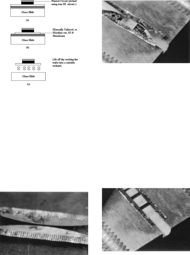
1.Metalization of the printed circuit is photolithographically de®ned and then etched in a beaker of heated and strongly agitated iron III nitrate solution, Figure 3~a!.
J. Microlith., Microfab., Microsyst., Vol. 1 No. 2, July 2002 151
Downloaded From: http://nanolithography.spiedigitallibrary.org/ on 05/19/2015 Terms of Use: http://spiedl.org/terms
Liu, Steenson, and Steer: Organic micromachining . . .
Fig. 3 Steps for realization of a membrane-based printed circuit from the copper-on-membrane board in Fig. 2.
2.Active devices, if necessary, are either wire bonded or chip attached onto the printed circuit as depicted in Figure 1~c!.
3.The membrane is then manually cut ~or cut using a laser! under a microscope to the design speci®cation, Figure 3~b!.
4.The membrane together with the printed circuit is then lifted off the glass slide by soaking the whole wafer in an organic solvent such as acetone, Figure 3~c!.
This membrane-supported printed circuit may be mounted in a waveguide or on a planar supporting frame. The waveguide or the supporting frame can be fabricated using organic-based microfabrication, as described elsewhere.10
Fig. 5 Finline resonator 1.8 mm in length shown mounted in half of a split block W-band waveguide with membrane thickness of around 8 mm and metal thickness of around 4 mm.
4 Experimental Results
A range of membrane-supported E-plane circuits has been realized on 5 mm thick membranes, Figures 4 ± 6, using the previously described technologies. Figure 4 shows two back-to-back waveguide-to-®nline transitions mounted in the E-plane ~across the short dimension! of a W-band waveguide fabricated as split blocks also using organic-based micromachining.10 The measurements in Figure 7 indicate a loss of around 0.4 dB/cm across the W band with a return loss of around 20 dB or better.
A ®nline resonator is shown in Figure 5 that is mounted on one side of a split block waveguide. Experimental characterization of the resonator in Figure 8 indicates a Q factor, as re¯ected by S21, of higher than 100.
Finally, an E-plane band pass ladder ®lter realized on an organic membrane ®n is shown in Figure 6. The S-parameter measurements shown in Figure 9 indicate a pass band insertion loss of around 0.5 dB.
According to a series of S-parameter measurements on membrane-supported components, the transmission loss was found to be typically less than 0.45 dB/cm across the
Fig. 4 Pair of back-to-back membrane-supported ®nline-to- waveguide transitions.
152 J. Microlith., Microfab., Microsyst., Vol. 1 No. 2, July 2002
Fig. 6 E-plane ladder band pass ®lter shown mounted in half of a split block waveguide with membrane thickness of around 8 mm and metal thickness of around 4 mm.
Downloaded From: http://nanolithography.spiedigitallibrary.org/ on 05/19/2015 Terms of Use: http://spiedl.org/terms

Liu, Steenson, and Steer: Organic micromachining . . .
Fig. 7 Measured S parameters of the two ®nline-to-waveguide transitions connected back to back in Fig. 8.
Fig. 9 Measured S parameters of a band pass ®lter with the pass band frequency centered at 107 GHz.
W band. The guide wavelength in all cases was found to be very close to the free space wavelength, suggesting that the dielectric effects on the E-plane circuit are virtually negligible. More importantly, matching the guide wavelength to the free-space wavelength considerably relaxes dimensional tolerances.
5 Discussion and Conclusions
The copper-on-membrane board depicted in Figure 2 is not the only version possible. Other variations can be formed with minor changes in processing. For instance, if the photosensitive organic membrane and the silver layer are interchanged in position, and if the photosensitive organic has not been exposed to ultraviolet light, it is possible to fabricate double-sided planar components, high-Q E-plane resonators and even electromagnetic band gap structures.
We have presented a handful of organic-membrane micromachining techniques. Particular reference was given to a simple copper-on-membrane board technology that enabled a membrane-supported printed circuit to be realized on a 5 mm thick membrane without any thermal processing.
Fig. 8 Measured S parameters of a ®nline resonator with resonant frequency581.5 GHz and resonator length51.8 mm.
Membrane-supported planar circuits can be easily implemented in this technology with conventional clean-room facilities in much the same manner as etching a printed circuit board on a standard substrate. The ®nal membranesupported components are both optically smooth and selfsupporting. It has been experimentally demonstrated that the transmission losses of components in all organicmembrane micromachining technologies are around 0.5 dB/cm.
References
1.P. J. Meier, ``Wideband subharmonically pumped W-band mixer in
single-ridge ®n-line,'' IEEE MTT-S Int. Microwave Symp. Dig. 1, 201±203 ~1982!.
2.V. M. Lubecke, K. Mizuno, and G. M. Rebeiz, ``Micromachining for
terahertz applications,'' IEEE Trans. Microwave Theory Tech. 46, 1821±1831 ~1998!.
3.R. M. Henderson and L. P. B. Katehi, ``Silicon-based micromachined
packages for high-frequency applications,'' IEEE Trans. Microwave Theory Tech. 47, 1563±1569 ~1999!.
4.M. Stotz, G. Gottwald, H. Haspeklo, and J. Wenger, ``Planar
millimeter-wave antennas using SiNx membranes on GaAs,'' IEEE Trans. Microwave Theory Tech. 44, 1593±1595 ~1996!.
5.R. M. Henderson, T. M. Weller, and L. P. B. Katehi, ``Three-
dimensional, W-band circuits using Si micromachining,'' IEEE MTT-S Int. Microwave Symp. Dig. 2, 441± 444 ~1999!.
6.J.-F. Kiang, ``Characteristic impedance of microshield lines with arbi-
trary shield cross section,'' IEEE Trans. Microwave Theory Tech. 46, 1328 ±1331 ~1998!.
7.G. Sajin, E. Matei, and M. Dragoman, ``Microwave straight edge resonator ~SER! on silicon membrane,'' IEEE MTT-S Int. Microwave Symp. Dig. 1, 283±286 ~1999!.
8.J. W. Digby et al., ``Fabrication and characterization of micromachined rectangular waveguide components for use at millimeter-wave
and terahertz frequencies,'' IEEE Trans. Microwave Theory Tech. 48, 1393±1302 ~2000!.
9.W. Y. Liu, D. P. Steenson, and M. B. Steer, ``Membrane-supported
copper E-plane circuits,'' IEEE MTT-S Int. Microwave Symp. Dig. 3, 539±542 ~2001!.
10.W. Y. Liu, D. P. Steenson, and M. B. Steer, ``Membrane-supported
CPW, with mounted active devices,'' IEEE Microwave Guid. Wave Lett. 11, 167±171 ~2001!.
11.W. Y. Liu, D. P. Steenson, and M. B. Steer, ``A technique of micro-
machining suitable for fabrication of submillimeter wave components,'' Proc. SPIE 4088, 144 ±177 ~Sept. 2000!.
12.W. Y. Liu, ``Novel technique of thin photoresist micromachining for submillimeter wave circuits,'' Proc. SPIE 4176, 28 ~Sept. 2000!.
13.W. Y. Liu, D. P. Steenson, and M. B. Steer, ``A simple but novel
technique of micromachining for millimeter wave and submillimeter wave applications,'' IWMF'2000 Workshop ~Oct. 2000!.
J. Microlith., Microfab., Microsyst., Vol. 1 No. 2, July 2002 153
Downloaded From: http://nanolithography.spiedigitallibrary.org/ on 05/19/2015 Terms of Use: http://spiedl.org/terms