

диафрагмированные волноводные фильтры / b0b57036-0482-48fc-8baa-0683bd585b25
.pdf868 |
IEEE TRANSACTIONS ON MICROWAVE THEORY AND TECHNIQUES, VOL. 67, NO. 3, MARCH 2019 |
Vertical LTCC Integrated Rectangular Waveguide and Transitions for Millimeter-Wave Applications
Aria Isapour , Graduate Student Member, IEEE, and Ammar Kouki
 , Senior Member, IEEE
Abstract— A new vertical guiding structure in low-temperature cofired ceramics (LTCC) substrates is proposed. This vertical LTCC integrated waveguide (V-LIW) allows transmitting signals and realizing components in the body of the LTCC substrate perpendicular to its surface. This vertical integration leads to considerable footprint reduction while opening the door to higher frequency coverage as well as easy implementation of E-plane structures. Discontinuities in V-LIW and transitions between the proposed V-LIW and conventional horizontal guiding structures such as coplanar waveguides, standard rectangular waveguides, and substrate integrated waveguides are also introduced. Applications to the design of V-band and W-band filters, couplers, and power dividers are presented. Several prototypes are fabricated with measurement results showing a good agreement with simulation data.
Index Terms— Coupler, filter, low-temperature cofired ceramic (LTCC), millimeter wave (mm-wave), power divider, substrate integrated waveguide (SIW), T-junction, 3-D, V-band.
I. INTRODUCTION
THE rapid progress of multifunctional hand-held devices in a context of growing number of wireless applications and cloud-based services leads to a daily increase in demand
for more bandwidth. The crowded microwave radio spectrum has limited bandwidth for today’s multitude of wireless services and cannot provide a long-term solution for the increasing bandwidth demands. It is, therefore, an unavoidable necessity to migrate to millimeter-wave (mm-wave) frequencies where we can take advantage of both large available bandwidth and less crowded channels.
In mm-wave frequencies, the loss of conventional planar guiding structures, e.g., microstrip, CPW, and stripline are significant. On the other hand, air-filled metallic waveguides show better loss performance but at the expense of bulkiness and integration complexity. Substrate integrated waveguides (SIWs) [1] offer a viable alternative through printed guiding structures to combine the low-loss performance of conventional rectangular waveguides with integration convenience of printed planar transmission lines. Since [1], in a large body of literature, researchers have explored SIW’s characteristics
Manuscript received November 28, 2017; revised April 1, 2018 and November 23, 2018; accepted November 29, 2018. Date of publication February 5, 2019; date of current version March 5, 2019. (Corresponding author: Aria Isapour.)
The authors are with the Communications and Microelectronic Laboratory, École de Technologie Supérieure, Montreal, QC H3C 1K3, Canada (e-mail: ammar.kouki@etsmtl.ca).
Color versions of one or more of the figures in this paper are available online at http://ieeexplore.ieee.org.
Digital Object Identifier 10.1109/TMTT.2019.2892743
such as design considerations [2], loss mechanism [3], and transitions [4], as well as the analytical [5] and numerical [6] modeling of SIW. Moreover, SIWs are widely used in the realization of a wide variety mm-wave circuits, e.g., filters [7], phase shifters [8], antennas [9], and so on.
Despite the interesting features of SIW, it still suffers from certain limitations and drawbacks. One of the most important ones is the implementation difficulty at very high frequencies. It is well known that the realization of certain conventional SIW circuits like magnetic coupling iris filters at frequencies of higher than 150 GHz with current ceramic fabrication technology is challenging and requires special designs like the one in [10] and [11]. This is due to the fact that the SIW relies on a set of vias to form waveguide side walls and also to perturb the fields inside the waveguide in applications like iris filters. The spacing between the adjacent in the same layer at higher frequencies would be too small to be fabricated with a regular multilayer ceramic process. Furthermore, SIW circuits, compared to their counterparts, usually use more footprints to realize components. This leads to a significant reduction of space for potential active circuits which can only be mounted on the surface. Moreover, for waveguide applications where E-plane structures are needed, conventional SIW cannot be utilized in a standard fabrication process. In these applications, metallic rectangular waveguides are still widely used as an H -plane-to-E-plane transitions [12].
In recent years, 3-D SIW structures were introduced to realize E-plane components [13] to make the mm-wave systems more compact [14]–[16] and reduce the footprint size [17]. However, all the reported works in [13]–[17] do so by a Lego-like assembling of one PCB substrate perpendicular to another substrate, which is not a standard PCB process, and therefore, structures are subjected to lateral misalignment and gaps between pieces [14], [16]. In fact, these 3-D SIWs are two conventional SIWs that are only attached together in an L-type configuration. These designs are also relatively bulky since the region between two sections of SIW is unusable.
Multilayer fabrication technologies, including lowtemperature cofired ceramic (LTCC) technology, are well suited for the implementation of SIWs [18] and they can be an excellent candidate to realize the 3-D SIWs as well. The well-established fabrication process of LTCC allows us to realize passive circuits by the almost arbitrary number of layers having very low-loss and high-permittivity dielectrics. Moreover, the relatively low sintering temperature makes it possible to utilize the high-conductivity metals; gold and silver. These all together enable LTCC to be a superior
0018-9480 © 2019 IEEE. Personal use is permitted, but republication/redistribution requires IEEE permission. See http://www.ieee.org/publications_standards/publications/rights/index.html for more information.

ISAPOUR AND KOUKI: V-LIW AND TRANSITIONS FOR mm-WAVE APPLICATIONS |
869 |
Fig. 1. V-LIW versus conventional SIW.
choice in the design of high-performance 3-D passive |
|
|
|
components from microwave frequencies [19] to optical [20] |
Fig. 2. |
Main building blocks in a waveguide system. |
|
and from exclusively packaging [21] to realize the entire RF |
|||
|
|
||
module [22], [23]. |
A. V-LIW Structure’s Basics |
||
In this paper, we propose a new type of LTCC integrated |
|||
|
|
||
waveguide (LIW) suitable for realizing true 3-D SIW struc- |
In the LTCC process, each layer of green tapes can have |
||
tures at mm-waves and beyond and for their eventual mass |
a different combination of filled vias and printed metallic |
||
production. In particular, we will introduce vertical LIW |
lines. Thanks to the powerful laser processing, as long as |
||
(V-LIW) structures and building blocks that can be fabricated |
the mechanical integrity of green tapes is preserved, the vias |
||
using a standard LTCC process and we show how they can be |
can have almost arbitrary shapes. To have a perfect vertical |
||
used to implement various functions at mm-wave frequencies. |
dielectric-filled rectangular waveguide, four rectangular vias |
||
Combined with horizontal SIW-type guides when needed, |
are required to form the side and the broad walls. However, |
||
complex functionality, including E-plane structures, can be |
this leads to the complete detachment of the dielectric between |
||
implemented over limited surface areas. The rest of this |
vias. Thus, in the proposed V-LIW, two rectangular vias are |
||
paper is organized as follows. Section II describes the V-LIW, |
used as the broad walls, while the two other vias replaced |
||
provides an empirical formula to find the propagation constant |
with printed metallic strips. Fig. 3(a) illustrates the geometry |
||
and cutoff frequency, and explains the loss mechanism and |
of each of these green tapes. As it can be seen from this |
||
design consideration. Section III presents proposed transitions |
figure, two rectangular vias are punched in each layer and |
||
to standard waveguides and planar transmission lines. These |
then filled with silver paste. The metal residues leaves around |
||
transitions are the essential parts for measurement purpose |
each via during via filling process are cleaned using a laser |
||
as well as circuit realization. In Section IV, the interesting |
process. Thereafter, the strips are printed on each layer. These |
||
features of V-LIW in the design of mm-waves passive circuits |
filled and printed layers are then stacked precisely with four |
||
through design will be demonstrated through simulation and |
alignment points to form the proposed 3-D guiding structure. |
||
successful measurement of three elementary circuits: a power |
With the aid of the proposed guiding structure, we can |
||
divider, a coupler, and two filters. Finally, conclusions are |
transfer signals vertically to the buried ceramic layers and |
||
given in Section V. |
also |
realize passive components in a perpendicular plane |
|
|
to the surface. The introduced V-LIW will address all the |
||
II. V-LIW STRUCTURE AND DESIGN CONSIDERATIONS |
limitations and drawbacks of conventional SIW and Lego- |
||
like 3-D SIWs, mentioned earlier in Section I. It will not |
|||
|
|||
At mm-wave frequencies, the wavelength becomes suffi- |
only significantly reduce the footprint size of the components |
||
ciently small to make it possible to realize a number of distrib- |
and save the circuit’s surface for mounting active components |
||
uted circuits vertically rather than horizontally. The basic ele- |
but also it will allow for easy implementation of E-plane |
||
ment of such vertical circuits is a new guiding structure which |
structures. Moreover, the proposed V-LIW can push the upper |
||
can transfer mm-wave signals in a perpendicular direction to |
frequency limit of realizing passive components with SIW. |
||
the surface. Fig. 1 illustrates how such a structure can be |
In our proposed V-LIW, printed metallic strips are used instead |
||
realized in a multilayer printed circuit technology, particularly |
of vias. These metallic strips can be as close as 18.5 μm to |
||
LTCC, and compares the proposed V-LIW structure to the |
each other and enable V-LIW to potentially operate at much |
||
conventional SIW alternative. However, in order to design and |
higher frequencies and eventually in terahertz frequencies. |
||
build meaningful circuits and functions, a number of building |
The working mechanism of V-LIW is very similar to its |
||
blocks are required in addition to the V-LIW. The main such |
antecedents, rectangular waveguide, and SIW; however, utiliz- |
||
building blocks are illustrated in Fig. 2 and will be addressed |
ing the metallic strips instead of continuous side walls or vias |
||
in the subsequent sections of this paper. |
could |
change its properties and the design considerations. |
|

870 |
|
|
|
|
IEEE TRANSACTIONS ON MICROWAVE THEORY AND TECHNIQUES, VOL. 67, NO. 3, MARCH 2019 |
||||||||||||||||||||||||||||
|
|
|
|
|
|
|
|
|
|
|
|
|
|
|
|
|
|
|
|
|
|
|
|
|
|
|
|
|
|
|
|
|
|
|
|
|
|
|
|
|
|
|
|
|
|
|
|
|
|
|
|
|
|
|
|
|
|
|
|
|
|
|
|
|
|
|
|
|
|
|
|
|
|
|
|
|
|
|
|
|
|
|
|
|
|
|
|
|
|
|
|
|
|
|
|
|
|
|
|
|
|
|
|
|
|
|
|
|
|
|
|
|
|
|
|
|
|
|
|
|
|
|
|
|
|
|
|
|
|
|
|
|
|
|
|
|
|
|
|
|
|
|
|
|
|
|
|
|
|
|
|
|
|
|
|
|
|
|
|
|
|
|
|
|
|
|
|
|
|
|
|
|
|
|
|
|
|
|
|
|
|
|
|
|
|
|
|
|
|
|
|
|
|
|
|
|
|
|
|
|
|
|
|
|
|
|
|
|
|
|
|
|
|
|
|
|
|
|
|
|
|
|
|
|
|
|
|
|
|
|
|
|
|
|
|
|
|
|
|
|
|
|
|
|
|
|
|
|
|
|
|
|
|
|
|
|
|
|
|
|
|
|
|
|
|
|
|
|
|
|
|
|
|
|
|
|
|
|
|
|
|
|
|
|
|
|
|
|
|
|
|
|
|
|
|
|
|
|
|
|
|
|
|
|
|
|
|
|
|
|
|
|
|
|
|
|
|
|
|
|
|
|
|
|
|
|
|
|
|
|
|
|
|
|
|
|
|
|
|
|
|
|
|
|
|
|
|
|
|
|
|
|
|
|
|
|
|
|
|
|
|
|
|
|
|
|
|
|
|
|
|
|
|
|
|
|
|
|
|
|
|
|
|
|
|
|
|
|
|
|
|
|
|
|
|
|
|
|
|
|
|
|
|
|
|
|
|
|
|
|
|
|
|
|
|
|
|
|
|
|
|
|
|
|
|
|
|
|
|
|
|
|
|
|
|
|
|
|
|
|
|
|
|
|
|
|
|
|
|
|
|
|
|
|
|
|
|
|
|
|
|
|
|
|
|
|
|
|
|
|
|
|
|
|
|
|
|
|
|
|
|
|
|
|
|
|
|
|
|
|
|
|
|
|
|
|
|
|
|
|
|
|
|
|
|
|
|
|
|
|
|
|
|
|
|
|
|
|
|
|
|
|
|
|
|
|
|
|
|
|
|
|
|
|
|
|
|
|
|
|
|
|
|
|
|
|
|
|
|
|
|
|
|
|
|
|
|
|
|
|
|
|
|
|
|
|
|
|
|
|
|
|
|
|
|
|
|
|
|
|
|
|
|
|
|
|
|
|
|
|
|
|
|
|
|
|
|
|
|
|
|
|
|
|
|
|
|
|
|
|
|
|
|
|
|
|
|
|
|
|
|
|
|
|
|
|
|
|
|
|
|
|
|
|
|
|
|
|
|
|
|
|
|
|
|
|
|
|
|
|
|
|
|
|
|
|
|
|
|
|
|
|
|
|
|
|
|
|
|
|
|
|
|
|
|
|
|
|
|
|
|
|
|
|
|
|
|
|
|
|
|
|
|
|
|
|
|
|
|
|
|
|
|
|
|
|
|
|
|
|
|
|
|
|
|
|
|
|
|
|
|
|
|
|
|
|
|
|
|
|
|
|
|
|
|
|
|
|
|
|
|
|
|
|
|
|
|
Fig. 3. (a) Multilayer LTCC process forming V-LIW. (b) Geometry of V-LIW after stacking.
Thus, in the following sections, we will discuss the main properties of a guiding structure: propagation constant, cutoff frequency, and loss performance.
B. Propagation Constant and Cutoff Frequency
Fig. 4. Comparison between phase constant of equivalent rectangular waveguide and simulated of V-LIW in V-band.
Fig. 3(b) depicts the geometry model of V-LIW with all |
|
|
|
|
|
|
|
|
|
|
|
|
|
|
|
||||
impactful parameters. It should be noted that in this geometry, |
|
|
|
|
|
|
|
|
|
|
|
|
|
|
|
||||
and also throughout this paper where it is |
not essential, |
|
|
|
|
|
|
|
|
|
|
|
|
|
|
|
|||
the dielectric is made transparent to show more details of |
|
|
|
|
|
|
|
|
|
|
|
|
|
|
|
||||
the designs. The discontinuities of side walls, realized by |
|
|
|
|
|
|
|
|
|
|
|
|
|
|
|
||||
metallic slots, have an impact on the propagation constant |
|
|
|
|
|
|
|
|
|
|
|
|
|
|
|
||||
and consequently on the cutoff frequency of the waveguide. |
|
|
|
|
|
|
|
|
|
|
|
|
|
|
|
||||
This impact can be simulated with full-wave finite-element |
|
|
|
|
|
|
|
|
|
|
|
|
|
|
|
||||
commercial software such as HFSS and HFWorks. It should |
|
|
|
|
|
|
|
|
|
|
|
|
|
|
|
||||
be noted that like any other SIW structure, since the current on |
|
|
|
|
|
|
|
|
|
|
|
|
|
|
|
||||
the side walls cannot be continuous, the V-LIW only supports |
Fig. 5. Comparison between phase constant of equivalent rectangular |
||||||||||||||||||
the propagation of TEn0 modes. The phase constant for the |
waveguide and simulated of V-LIW in W-band. |
|
|
|
|||||||||||||||
dominant mode of V-LIW, TE10, can be calculated from the |
|
|
|
|
|
|
|
|
|
|
|
|
|
|
|
||||
phase difference between the transmission coefficients of two |
expression: |
|
|
|
|
|
|
|
|
|
|
||||||||
lengths of a line, given by [24] |
− L2 . |
|
+ |
|
|
|
|
|
|
|
|
|
|||||||
βSIW = |
L1 |
(1) |
|
eq |
= |
|
|
|
|
|
a |
|
|
|
|
|
|||
|
S21L2 |
− |
S21L1 |
|
a |
|
|
a |
0.995 |
|
0.2017 |
h − t |
|
|
|
|
|
||
|
|
|
|
|
|
|
|
|
|
|
|
|
|
|
2 |
|
|
2 |
|
Furthermore, the cutoff frequency of V-LIW can be found |
|
|
|
|
|
|
|
|
|
h − t |
|
0.005 t |
|
||||||
by calculating the propagation constant for different frequen- |
|
|
|
|
|
|
+ |
0.7748 |
|
+ |
|
(2) |
|||||||
|
|
|
|
|
|
|
|
a |
|
h |
|
|
|||||||
cies and finding the frequency in which the real and imaginary |
|
|
|
|
|
|
|
|
|
|
|
|
|
||||||
parts of the propagation |
constant |
are equal |
[3]. However, |
where aeq is the equivalent rectangular waveguide width, a is |
|||||||||||||||
it would be beneficial to find the equivalent rectangular |
the actual width of V-LIW, t is the thickness of printed metals, |
||||||||||||||||||
waveguide width as a function of V-LIW’s parameters in order |
and h is the gap between two consecutive printed strips, which |
||||||||||||||||||
to estimate the phase constant of V-LIW in the guiding region |
equals the product of the number of layers between them and |
||||||||||||||||||
to facilitate the analysis of this guiding structure. Later, this |
the thickness of each layer. To verify the accuracy of (2), |
||||||||||||||||||
equivalent waveguide can be used in all design processes |
the phase constant for two different frequency bands, V-band |
||||||||||||||||||
before the final simulation. An empirical expression in [25] |
and W-band, and also for two different widths of V-LIW is |
||||||||||||||||||
and a theoretical formula in [5] have been |
presented for |
simulated and plotted in Figs. 4 and 5 along with the phase |
|||||||||||||||||
the equivalent rectangular waveguide width of the conven- |
constant for rectangular waveguides with equivalent widths |
||||||||||||||||||
tional SIWs with cylindrical vias; however, those cannot be |
given by (2). It should be noted that the chosen dielectric |
||||||||||||||||||
used here due to too many differences in the shape of vias |
for V-band and W-band are Dupont 9k7 (εr : 7.1) and Ferro |
||||||||||||||||||
between our work and those. In order to find the equivalent |
A6M (εr : 6.21), respectively. As we can see in Figs. 4 and 5, |
||||||||||||||||||
width, the propagation constant for a series of V-LIWs with |
results are in good agreement. In fact, (2) provides a precision |
||||||||||||||||||
different geometries has been calculated, then the width of |
better than 0.2% in the nondispersive region and it is valid for |
||||||||||||||||||
rectangular waveguides that produce the same propagation |
h λg /2. It should be noted that for the case, t equals h, |
||||||||||||||||||
constants has been found, and finally, an empirical formula |
aeq |
approaches a. This behavior follows our expectation from |
|||||||||||||||||
for equivalent width has been obtained by applying the least |
the geometry of our integrated waveguide, where the V-LIW |
||||||||||||||||||
square approach [26]. This procedure leads to the following |
becomes a simple rectangular waveguide. |
|
|
|
|||||||||||||||

ISAPOUR AND KOUKI: V-LIW AND TRANSITIONS FOR mm-WAVE APPLICATIONS |
871 |
Fig. 6. |
Attenuation constants for a V-LIW at V-band. a: |
1340 |
μm, |
b: 700 μm, h: 224 μm, t: 8 μm, and surface roughness: 2 μm. |
|
|
|
Fig. 7. Radiation loss for a V-LIW as a function of the pitch of printed strips normalized to the wavelength at 60 GHz. a: 1340 μm, b: 700 μm, h: 224 μm, t: 8 μm, and surface roughness: 2 μm.
C. Loss Mechanism
RF signals passing through the V-LIW are attenuated due to losses. αT is the total attenuation constant of V-LIW and like any other guiding structure, it has three parts: conductor loss (αC ), dielectric loss (αD ), and radiation loss (αR )
αT = αC + αD + αR . |
(3) |
The first two parts are due to the lossy materials with which the V-LIW is constructed and they are almost identical to the ones for the conventional filled rectangular waveguide with the same dimensions and materials, given by [27]
αD = |
k2tanδ |
|
|
(4) |
2β |
|
|||
αC = |
Rs |
(2bπ 2 + a3k2) |
(5) |
|
a3bβkη |
||||
where k is the wavenumber of the unbounded homogeneous medium, β is the propagation constant, Rs is the surface resistivity, tan δ is the dielectric loss tangent of LTCC green tapes, and η is the intrinsic impedance of the waves in the dielectric.
For LTCC systems with crystallizing dielectric like DuPont 9k7 and Ferro A6M, which are usually used in the mm-waves, the dielectric loss tangent at frequencies around 60 GHz is about 0.001±0.0005 leads to a dielectric loss about 0.2 dB/cm from (4). Furthermore, the metals in LTCC systems are usually silver and gold with the conductivity of 6.1×10⁷ and 4.1×10⁷, respectively. The conductor loss factor for these conductivities lies in about 0.15 dB/cm using (5).
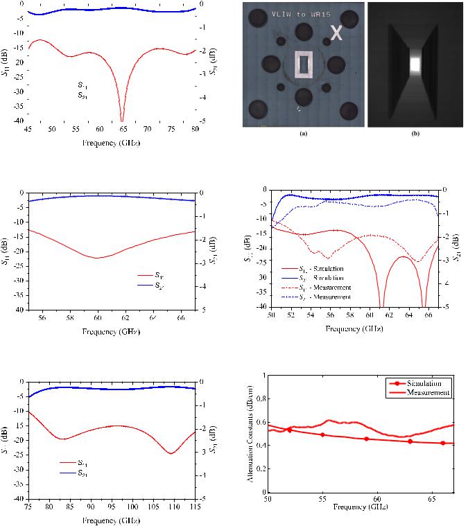
Radiation loss, unlike conductor and dielectric loss, depends on the form and geometry of the waveguide. Since the V-LIW is not a closed structure and it does not have complete walls on all sides, a part of traveling signal radiates from the gaps between the slots forming the side walls. In order to calculate radiation loss, one can use numerical methods or full-wave simulation software. The attenuation constants, extracted from simulation, for a V-LIW designed for V-band is illustrated in Fig. 6.
For this waveguide, which is a practical V-LIW of interest, the radiation loss is almost zero. However, if the pitch of
printed strips increases, by increasing the number of layers between the printed strips or using thicker LTCC layers, the radiation loss will increase. Nominal LTCC tape thickness ranges from 20 to 300 μm for single tapes. To assess the impact of spacing between strips on radiation, Fig. 7 shows the simulated radiation loss versus the normalized spacing between strips (h) at 60 GHz, the mid-band frequency at V-band. From Fig. 7 and with the previous knowledge that the conductor and the dielectric losses are about 0.2 and 0.1 dB/cm, respectively, we can find that the pitch should be smaller than the quarter of wavelength before the radiation loss becomes dominant. This condition could be always met without difficulty; noticing that the thickness of LTCC green tapes is usually less than 300 μm which is much smaller than the wavelength in mm-wave frequencies. On the other hand, considering that 20-μm LTCC green tapes (Ferro A6M) have recently been available, the proposed V-LIW potentially works up to 1.5 THz before the radiation loss becomes dominant. Fig. 7 shows different regions of V-LIW operation when the spacing between printed metalic strips increases. In this plot, the guiding region is the region where radiation loss is not dominant and is less than conductor and dielectric losses. The leakage region is the region where the radiation part is larger than the conductor and dielectric loss by several orders and V-LIW can be used in the design of applications like an antenna. Between these two regions, the structure has radiation losses too high to be a viable waveguide and too low to be a leaky-wave antenna. This region, known as the forbidden region [3], should be avoided.
III. V-LIW CIRCUITS BUILDING BLOCKS
In order to use V-LIW interconnections in an mm-wave system and also to be able to realize V-LIW passive circuits, certain building blocks that are commonly utilized in numerous communication systems are introduced here. These blocks include the following: 1) transition from WR15 (WR10), standard waveguide for V-band (W-band), to the V-LIW; 2) transition from CPW to V-LIW; 3) transition from conventional horizontal LIW (H-LIW) to the V-LIW (90◦ bend);
872 IEEE TRANSACTIONS ON MICROWAVE THEORY AND TECHNIQUES, VOL. 67, NO. 3, MARCH 2019
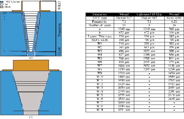
TABLE I
PARAMETERS OF V-LIW TO THE STANDARD WAVEGUIDES TRANSITION
Fig. 8. Geometry of transition from standard waveguides to V-LIW. (a) Front view. (b) Side view.
and 4) T-junction. A back-to-back transition from CPW to V-LIW, which is essentially a combination of transitions 2) and 3), is also presented.
A. Transition From V-LIW to Standard Waveguides
Waveguide adaptors are widely used to connect mm-wave components to measuring equipment. These adaptors essentially consist of pieces of hollow waveguides and a flange for joining sections. The dimensions of these hollow waveguides are generally identical to the standard waveguide for the desired band of frequency. A transition from the proposed V-LIW to those empty standard waveguide should, therefore, be considered for measurement by these adaptors.
For the same cutoff frequency, the dimension of V-LIW and the standard waveguide are very different, since the V-LIW is a type of high-permittivity dielectric-filled waveguide contrary to standard air-filled waveguides. Thus, to have a smooth transition, the dimensions of the waveguide should progressively be increased and also the dielectric should gradually be removed.
The geometry of the designed transition is illustrated in Fig. 8. This transition is designed for V-band frequencies and it consists of 19 LTCC green tape layers, with the thickness of 224 μm each. The width and height of the waveguide are linearly increased in each layer to go from V-LIW’s width and height to the ones for WR15, the V-band standard waveguide. As a starting point, the dimension of cavities can be selected by the Klopfenstein impedance taper
method [27] for the transition of the wave impedance from V-LIW to WR15. It should be noted that for the desired ripple of bandwidth, there is a minimum length to be able to use Klopfenstein design equations. This condition is satisfied for our designed transitions. Klopfenstein method guarantees the optimum return loss for a given taper length [27]; however, it is not true in our case. This is because there are unavoidable slabs of dielectric next to the rectangular vias, which are needed for the mechanical integrity of the structure in the fabrication process. These slabs make it impossible to realize the required impedance, needed by Klopfenstein method, in the last several layers toward the standard waveguide. Therefore, the dimensions of the cavities should be optimized to obtain the best result.
It should be noted that if one is interested only in a portion of the band, not the entire V-band, the length of transition could be significantly smaller. In order to show this, here we also optimized this transition with only eight LTCC layers for operating frequencies from 57 to 64 GHz, which is a very popular unlicensed band of interest in V-band. Furthermore, the same type of transition in W-band, from V-LIW to WR10, is designed and simulated. All optimized dimensions for these three transitions are listed in Table I, and the simulation results are shown in Figs. 9–11. It should be noted that although this transition shows good performance on the entire band, they are still subject to all limitations and drawbacks of rectangular waveguide like dispersion region and higher order modes.
A pair of optimized transition for V-band frequencies has been fabricated and measured in a back-to-back configuration using WR15 waveguide adaptors and N5247A PNA-X network analyzer. Photographs of fabricated transition are shown in Fig. 12. A TRL calibration has been carried out to eliminate
ISAPOUR AND KOUKI: V-LIW AND TRANSITIONS FOR mm-WAVE APPLICATIONS |
873 |
|||||||||||||||||||
|
|
|
|
|
|
|
|
|
|
|
|
|
|
|
|
|
|
|
|
|
|
|
|
|
|
|
|
|
|
|
|
|
|
|
|
|
|
|
|
|
|
|
|
|
|
|
|
|
|
|
|
|
|
|
|
|
|
|
|
|
|
|
|
|
|
|
|
|
|
|
|
|
|
|
|
|
|
|
|
|
|
|
|
|
|
|
|
|
|
|
|
|
|
|
|
|
|
|
|
|
|
|
|
|
|
|
|
|
|
|
|
|
|
|
|
|
|
|
|
|
|
|
|
|
|
|
|
|
|
|
|
|
|
|
|
|
|
|
|
|
|
|
|
|
|
|
|
|
|
|
|
|
|
|
|
|
|
|
|
|
|
|
|
|
|
|
|
|
|
|
|
|
|
|
|
|
|
|
|
|
|
|
|
|
|
|
|
|
|
|
|
|
|
|
|
|
|
|
|
|
|
|
|
|
|
|
|
|
|
|
|
|
|
|
|
|
|
|
|
|
|
|
|
|
|
|
|
|
|
|
|
|
|
|
|
|
|
|
|
|
|
|
|
|
|
|
|
|
|
|
|
|
|
|
|
|
|
|
|
|
|
|
|
|
|
|
|
|
|
|
|
|
|
|
|
|
|
|
|
|
|
|
|
|
|
|
|
|
|
|
|
|
|
|
|
|
|
|
|
|
|
|
|
|
|
|
|
|
|
|
|
|
|
|
|
|
|
|
|
|
|
|
|
|
|
|
|
|
|
|
|
|
|
|
|
|
|
|
|
|
|
|
|
|
|
|
|
|
|
|
|
|
|
|
|
|
Fig. 9. Simulation results for transition from V-LIW to WR15 standard waveguide for V-band.
Fig. 12. Fabricated transition from V-LIW to the standard waveguide for V-band frequencies. (a) Top-view photograph. (b) X-ray photograph of inside of transition.
Fig. 10. Simulation results for transition from V-LIW to WR15 standard waveguide for unlicensed 60 GHz.
Fig. 13. Simulation and measurement results for back-to-back transition from V-LIW to WR15.
Fig. 14. Simulated and measured loss performance of a V-LIW transmission
line at V-band frequencies.
Fig. 11. Simulation results for transition from V-LIW to WR10 standard waveguide for W-band.
the effect of waveguide adaptors [28]. The measurement and simulation results for the entire back-to-back transitions are plotted in Fig. 13. Furthermore, this transition enables us to solely measure a V-LIW transmission line using TRL calibration at V-band and extract its loss performance. Fig. 14 shows the comparison of the simulated and measured loss
performance of fabricated V-LIW. Overall, the measured return loss is better than 15 dB from 63 to 67 GHz.
B. Transition From V-LIW to CPW
The interconnection between the V-LIW and other mmwave components such as active devices and MEMS switches usually requires a transition to planar transmission lines.

874 |
|
|
|
|
|
|
|
|
|
|
IEEE TRANSACTIONS ON MICROWAVE THEORY AND TECHNIQUES, VOL. 67, NO. 3, MARCH 2019 |
|||||||||||||||||||||||
|
|
|
|
|
|
|
|
|
|
|
|
|
|
|
|
|
|
|
|
|
|
|
|
|
|
|
|
|
|
|
|
|
|
|
|
|
|
|
|
|
|
|
|
|
|
|
|
|
|
|
|
|
|
|
|
|
|
|
|
|
|
|
|
|
|
|
|
|
|
|
|
|
|
|
|
|
|
|
|
|
|
|
|
|
|
|
|
|
|
|
|
|
|
|
|
|
|
|
|
|
|
|
|
|
|
|
|
|
|
|
|
|
|
|
|
|
|
|
|
|
|
|
|
|
|
|
|
|
|
|
|
|
|
|
|
|
|
|
|
|
|
|
|
|
|
|
|
|
|
|
|
|
|
|
|
|
|
|
|
|
|
|
|
|
|
|
|
|
|
|
|
|
|
|
|
|
|
|
|
|
|
|
|
|
|
|
|
|
|
|
|
|
|
|
|
|
|
|
|
|
|
|
|
|
|
|
|
|
|
|
|
|
|
|
|
|
|
|
|
|
|
|
|
|
|
|
|
|
|
|
|
|
|
|
|
|
|
|
|
|
|
|
|
|
|
|
|
|
|
|
|
|
|
|
|
|
|
|
|
|
|
|
|
|
|
|
|
|
|
|
|
|
|
|
|
|
|
|
|
|
|
|
|
|
|
|
|
|
|
|
|
|
|
|
|
|
|
|
|
|
|
|
|
|
|
|
|
|
|
|
|
|
|
|
|
|
|
|
|
|
|
|
|
|
|
|
|
|
|
|
|
|
|
|
|
|
|
|
|
|
|
|
|
|
|
|
|
|
|
|
|
|
|
|
|
|
|
|
|
|
|
|
|
|
|
|
|
|
|
|
|
|
|
|
|
|
|
|
|
|
|
|
|
|
|
|
|
|
|
|
|
|
|
|
|
|
|
|
|
|
|
|
|
|
|
|
|
|
|
|
|
|
|
|
|
|
|
|
|
|
|
|
|
|
|
|
|
|
|
|
|
|
|
|
|
|
|
|
|
|
|
|
|
|
|
|
|
|
|
|
|
|
|
|
|
|
|
|
|
|
|
|
|
|
|
|
|
|
|
|
|
|
|
|
|
|
|
|
|
|
|
|
|
|
|
|
|
|
|
|
|
|
|
|
|
|
|
|
|
|
|
|
|
|
|
|
|
|
|
|
|
|
|
|
|
|
|
|
|
|
|
|
|
|
|
|
|
|
|
|
|
|
|
|
|
|
|
|
|
|
|
|
|
|
|
|
|
|
|
|
|
|
|
|
|
|
|
|
|
|
|
|
|
|
|
|
|
|
|
|
|
|
|
|
|
|
|
|
|
|
|
|
|
|
|
|
|
|
|
|
|
|
|
|
|
|
|
|
|
|
|
|
|
|
|
|
|
|
|
|
|
|
|
|
|
|
|
|
|
|
|
|
|
|
|
|
|
|
|
Fig. 15. (a) Geometry of direct V-LIW-to-CPW transition (Transition 1).
(b) Section cut at AA. (c) Top view. Dimensions are given in μm.
Fig. 17. Simulation results for the transitions from V-LIW to CPW.
Fig. 16. (a) Geometry of V-LIW-to-CPW transition by one layer of half coax middle section (Transition 2). (b) Section cut at AA. (c) Top view. Dimensions are given in μm.
This transition can also be used to connect the V-LIW passive components to high-frequency CPW measurement probes.
Figs. 15 and 16 depict two proposed transitions from V-LIW to CPW. In these transitions, an L-shape loop is used to excite the TE10 mode of V-LIW and then this loop connects to a CPW line. These two transitions are almost the same except in the former, the CPW is directly connected to the V-LIW; on the other hand, in the latter, one layer of half coaxial line is used between V-LIW and CPW.
The idea of waveguides excitation with an L-shape loop has been previously used in the end-launcher coaxial to waveguides transitions [29]. As shown in Fig. 15, a viaprobe that is shorted to the body of V-LIW forms a current loop to excite magnetic fields of TE10 mode. The length and the position of this via-probe and also the length and the width of the shorting strip should be selected as such the transition provides the same impedance as the CPW line on the top. The analytical expression for real and imaginary parts of the input impedance in a waveguide entrance using the loop coupling model and the probe coupling model has been provided in [30] and [31]; however, since not every length of via-probes can be fabricated and we are limited to the discrete number of LTCC layers, an optimization using commercial software is required to obtain the best possible matching and return loss. The proposed transition has been simulated and optimized using ANSYS HFSS to operate at 60 GHz.
The optimized dimensions for these transitions considering the Dupont 9k7 tapes are shown in the geometry figures. The simulated scattering parameters of these transitions are illustrated in Fig. 17. As it is expected for a probe-type transition, about 10% fractional bandwidth is achieved. This is mainly because the inductance of the via-probe, which should be canceled during the transition, is highly frequency dependent. It should be noted that the optimized direct transition shows better return loss and it is good for the case where one wants to test a V-LIW component. On the other hand, the second transition with a half coaxial is more convenient than the first transition for integration with other components.
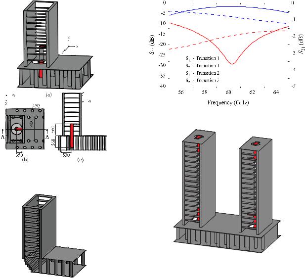
C. Transition From V-LIW to H-LIW
Completing V-LIW library to be used in microwave systems still needs another transition; a transition to conventional SIW which, for the sake of uniformity of notation, is called H-LIW here. This transition, which is essentially a 90◦ bend, along with the previous transition to CPW, enables us to transfer electromagnetic waves from the top layer to the buried layers using V-LIW and then bring it back to the top.
The geometry of the proposed transition is illustrated in Fig. 18. This transition consists of two parts: 1) the part in the V-LIW is an L-shape end-launcher transition which is discussed in the previous subsection and 2) the part in H-LIW which is a probe-type waveguide transition from the broad wall.
The operation mechanism of the proposed transition in the second part is based on the probe excitation of rectangular waveguides which is widely used in the design of coaxial-to- conventional waveguides transitions [32], [33] and also more recently in CPW-to-SIW transitions [34], [35]. In this type of transitions, a metallic probe rod operating as a monopole antenna excites the electric field inside the waveguide. This probe is placed vertically along to the smaller side of the waveguide to be parallel to electrical fields of TE10 mode [36]. Furthermore, a short-circuiting plane at a distance behind the probe is required to ensure the proper radiation in the waveguide propagation direction [33]. The distance for the case that we neglect the inductance of the probe is a quarter
ISAPOUR AND KOUKI: V-LIW AND TRANSITIONS FOR mm-WAVE APPLICATIONS |
875 |
|||||||||||||||||||||||||
|
|
|
|
|
|
|
|
|
|
|
|
|
|
|
|
|
|
|
|
|
|
|
|
|
|
|
|
|
|
|
|
|
|
|
|
|
|
|
|
|
|
|
|
|
|
|
|
|
|
|
|
|
|
|
|
|
|
|
|
|
|
|
|
|
|
|
|
|
|
|
|
|
|
|
|
|
|
|
|
|
|
|
|
|
|
|
|
|
|
|
|
|
|
|
|
|
|
|
|
|
|
|
|
|
|
|
|
|
|
|
|
|
|
|
|
|
|
|
|
|
|
|
|
|
|
|
|
|
|
|
|
|
|
|
|
|
|
|
|
|
|
|
|
|
|
|
|
|
|
|
|
|
|
|
|
|
|
|
|
|
|
|
|
|
|
|
|
|
|
|
|
|
|
|
|
|
|
|
|
|
|
|
|
|
|
|
|
|
|
|
|
|
|
|
|
|
|
|
|
|
|
|
|
|
|
|
|
|
|
|
|
|
|
|
|
|
|
|
|
|
|
|
|
|
|
|
|
|
|
|
|
|
|
|
|
|
|
|
|
|
|
|
|
|
|
|
|
|
|
|
|
|
|
|
|
|
|
|
|
|
|
|
|
|
|
|
|
|
|
|
|
|
|
|
|
|
|
|
|
|
|
|
|
|
|
|
|
|
|
|
|
|
|
|
|
|
|
|
|
|
|
|
|
|
|
|
|
|
|
|
|
|
|
|
|
|
|
|
|
|
|
|
|
|
|
|
|
|
|
|
|
|
|
|
|
|
|
|
|
|
|
|
|
|
|
|
|
|
|
|
|
|
|
|
|
|
|
|
|
|
|
|
|
|
|
|
|
|
|
|
|
|
|
|
|
|
|
|
|
|
|
|
|
|
|
|
|
|
|
|
|
|
|
|
|
|
|
|
|
|
|
|
|
|
|
|
|
|
|
|
|
|
|
|
|
|
|
|
|
|
|
|
|
|
|
|
|
|
|
|
|
|
|
|
|
|
|
|
|
|
|
|
|
|
|
|
|
|
|
|
|
|
|
|
|
|
|
|
Fig. 20. Simulation results for transition from V-LIW to H-LIW.
Fig. 18. Geometry of V-LIW-to-H-LIW transition. (a) 3-D view. (b) Top view. (c) Section cut at AA.
Fig. 21. Geometry of the back-to-back transition.
Fig. 19. Geometry of V-LIW-to-H-LIW corner transition.
wavelength, but in fact, for a practical case, it must be less than that to cancel out the inductance introduced by the probe rod. This distance along with the length, the diameter, and the off-center positioning of the via are the parameters of the transition that should be optimized to achieve a smooth transition from V-LIW to H-LIW. An experimental method to design this type of transition is presented in [32]. Furthermore, Mumford [37] showed that with only two of three parameters including length, off-center positioning, and distance to the short-circuiting plane of probe rod, one can match any impedance less than waveguide characteristic impedance. Moreover, a method to find optimum dimensions to provide the widest possible bandwidth for a waveguide to coaxial cable transition is provided in [37].
An alternative way to realize the transition from V-LIW to H-LIW is to make a quarter-wavelength corner using steps formed by rectangular vias (Fig. 19). This transition can provide us with better bandwidth. However, by respecting the minimum via-to-via spacing for our in-house LTCC process,
this transition has slightly more insertion loss due to small radiation from corners.
The proposed transition and the corner transition, considering Dupont 9k7 dielectric, have been optimized using ANSYS HFSS at 60 GHz. The simulation results are plotted in Fig. 20 and it shows that the optimized transitions cover the entire unlicensed band around 60 GHz. It should be noted that the passivity condition was checked and found to be satisfied for both transitions.
In order to examine the proposed transitions and verify the simulation results, a back-to-back structure consists of both transitions to CPW and H-LIW is designed and fabricated. As it is depicted in Fig. 21, this structure at both sides is terminated to the CPW lines and it can be easily measured using high-frequency CPW probes. The simulation and measurement results of the back-to-back transitions are plotted in Fig. 22, which shows a good agreement between simulation and fabrication.
D. V-LIW T-Junction
One of the main blocks in many communication systems such as feeding networks of antennas is a tee waveguide

876 |
|
|
|
|
IEEE TRANSACTIONS ON MICROWAVE THEORY AND TECHNIQUES, VOL. 67, NO. 3, MARCH 2019 |
||||||||||||||
|
|
|
|
|
|
|
|
|
|
|
|
|
|
|
|
|
|
|
|
|
|
|
|
|
|
|
|
|
|
|
|
|
|
|
|
|
|
|
|
|
|
|
|
|
|
|
|
|
|
|
|
|
|
|
|
|
|
|
|
|
|
|
|
|
|
|
|
|
|
|
|
|
|
|
|
|
|
|
|
|
|
|
|
|
|
|
|
|
|
|
|
|
|
|
|
|
|
|
|
|
|
|
|
|
|
|
|
|
|
|
|
|
|
|
|
|
|
|
|
|
|
|
|
|
|
|
|
|
|
|
|
|
|
|
|
|
|
|
|
|
|
|
|
|
|
|
|
|
|
|
|
|
|
|
|
|
|
|
|
|
|
|
|
|
|
|
|
|
|
|
|
|
|
|
|
|
|
|
|
|
|
|
|
|
|
|
|
|
|
|
|
|
|
|
|
|
|
|
|
|
|
|
|
|
|
|
|
|
|
|
|
|
|
|
|
|
|
|
|
Fig. 22. Simulation and measurement results of the back-to-back structure including both transitions from V-LIW to H-LIW and CPW.
Fig. 25. Geometry of V-LIW E-plane power divider. (a) Top view. (b) Side view.
Fig. 23. Geometry of E-plane V-LIW T-junction side view and matching wedge.
Fig. 24. Simulation results of a T-junction V-LIW.
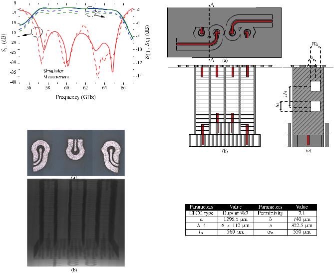
junction. Fig. 23 shows the geometry of an E-plane V-LIW T-junction, which is not easy to realize with conventional SIWs. In the middle arm of the proposed design, a three-layer pseudowedge is added. This pseudowedge helps to optimize the power division and minimize the return loss [38], [39].
The designed T-junction has been optimized for the unlicensed band around 60 GHz. The optimized scattering parameters of this structure are plotted in Fig. 24.
IV. V-LIW APPLICATION TO DESIGN PASSIVE CIRCUITS
The proposed V-LIW has been fully characterized in the previous sections together with the main building blocks that are required to realize almost every communication system. In this section, the V-LIW’s interesting features and capabilities will be demonstrated by designing and testing three frequently used passive components: an E-plane power divider, a coupler, and two filters.
A. V-LIW E-Plane Power Divider
The E-plane power divider, as a basic component, is widely used to introduce new guiding lines [40], [41]. As one of the interesting capabilities of our proposed V-LIW transmission line, we designed a highly compact antiphase E-plane T-junction power divider. The geometry of the designed power divider is illustrated in Fig. 25. This power divider is essentially a combination of a V-LIW T-junction, two 90◦ V-LIW bends, and the CPW-to-V-LIW transitions which are used in the input and output sections to conveniently measure the power divider with CPW probes. Moreover, a 90◦ CPW bend is attached to two of the outputs to facilitate probe alignment in the three-port measurement setup.
The designed power divider has been optimized to operate between 57 and 64 GHz; in the unlicensed segment of the V-band. The simulated and measured return loss and insertion loss are shown in Fig. 26. This figure shows that the designed power divider has a return loss of better than 14 dB (11.4 dB measured) over the entire unlicensed band. The simulation transmission loss from port 1 to port 2 and port 3 is 3.8 ± 0.1 in the desired band. An amplitude imbalance of ±0.05 dB (0.5 dB measured) and a phase imbalance of better than ±0.8◦ (0.8◦ measured) have been achieved for this power divider. Fig. 27 shows the top view and the X-ray photograph of the fabricated E-plane power divide.
ISAPOUR AND KOUKI: V-LIW AND TRANSITIONS FOR mm-WAVE APPLICATIONS |
877 |
|||||||||||||||||
|
|
|
|
|
|
|
|
|
|
|
|
|
|
|
|
|
|
|
|
|
|
|
|
|
|
|
|
|
|
|
|
|
|
|
|
|
|
|
|
|
|
|
|
|
|
|
|
|
|
|
|
|
|
|
|
|
|
|
|
|
|
|
|
|
|
|
|
|
|
|
|
|
|
|
|
|
|
|
|
|
|
|
|
|
|
|
|
|
|
|
|
|
|
|
|
|
|
|
|
|
|
|
|
|
|
|
|
|
|
|
|
|
|
|
|
|
|
|
|
|
|
|
|
|
|
|
|
|
|
|
|
|
|
|
|
|
|
|
|
|
|
|
|
|
|
|
|
|
|
|
|
|
|
|
|
|
|
|
|
|
|
|
|
|
|
|
|
|
|
|
Fig. 26. Scattering parameters of the V-LIW E-plane power divider. Solid lines: simulated results. Dashed lines: measured results.
Fig. 27. Fabricated E-plane power divide. (a) Top-view photograph.
(b) X-ray photograph of inside of LTCC.
B. V-LIW Multihole Bethe Directional Coupler
Another basic component that we have selected to implement by our new guiding structure is multihole Bethe coupler. This type of couplers consists of one or several small holes that couple the wave from a rectangular waveguide to another which have a broad wall in common [27]. The holes could be circles, rectangles, or any arbitrary shapes; however, we are limited to the rectangular holes for the implementation with V-LIW.
The designed V-LIW directional coupler in V-band frequencies is illustrated in Fig. 28. It is worth mentioning that to realize the apertures between the V-LIWs, we have partially drilled the rectangular vias in corresponding layers; thus, the nondrilled parts work like a coupling aperture between two waveguides.
In order to find the parameters in this geometry, we followed the design procedure presented in [27] with some modifications for the rectangular slot. Following this procedure, it can be found that the spacing between the center of the rectangular
Fig. 28. Geometry of V-LIW coupler. (a) Top view. (b) Side view.
(c) Section cut at AA.
TABLE II
PARAMETERS OF V-LIW COUPLER
slot and the center of the waveguide (s) should be a quarter of the waveguide’s width (a/4) to maximize the isolation. Subsequently, with this spacing, the coupling for two identical rectangular slots is given by
C(dB) = −20 log |
|
π εωβ2 |
− 20log 2la wa2 |
(6) |
|
16P10k2 |
|||||
where P10 is defined by |
|
|
|
|
|
|
|
|
|
|
|
P10 = |
abβ |
. |
(7) |
||
|
|||||
kη |
|||||
It should be noted that in the derivation of (6), the electric and magnetic polarizabilities of a rectangular slot are considered identical and equal to (1/16)πlawa2 [42]. Furthermore, since the spacing between two slots should be a quarter of the guided wavelength, we recommend selecting a width of the V-LIW for that the equivalent waveguide width provides us an integer number of layers for this spacing.
Table II lists the coupler’s optimized parameter to have a 20-dB coupling at 60 GHz. It is worth mentioning that we have only optimized the width of the slot which was 430 μm in the calculation. The difference is mainly because, in the derivation of the coupling factor, there is an estimation assuming the radiation from a small aperture in a thin metal layer between two waveguides, which is not the case here. Fig. 29 shows the photographs of the fabricated coupler with DuPont 9k7 dielectric. The simulation and measurement