

диафрагмированные волноводные фильтры / c6dbe12a-7386-4431-a9aa-cb635eeb67db
.pdfThis article has been accepted for publication in a future issue of this journal, but has not been fully edited. Content may change prior to final publication. Citation information: DOI 10.1109/TAP.2017.2717046, IEEE Transactions on Antennas and Propagation
1
Compact Singleand Dual-Band Filtering Patch Antenna Arrays Using Novel Feeding Scheme
Yao Zhang, Xiu Yin Zhang, Senior Member, IEEE, and Yong-Mei Pan, Member, IEEE
Abstract—This paper presents two compact patch antenna arrays using a novel feeding scheme to integrate bandpass responses. The two arrays have no filtering circuits but reveal high filtering performance. For each array, only a microstrip feed line is coupled to radiating patches and specific coupling regions are employed to obtain the desired current distribution on the radiating patches. In the operating band, the induced currents on the patches are in phase, resulting in high boresight gain. At the out-of-band frequencies, the patches are not excited or the induced currents on them are 180o out-of-phase, resulting in radiation suppression. Using this method, out-of-band radiation can be suppressed without degrading the in-band performance. For demonstration, a 4-element planar patch array is firstly implemented. Single-band bandpass response is observed in the experiment. Measured in-band gains are 12.6 dBi, whereas out-of-band suppression is more than 20 dB. Then the feeding scheme is employed to design two 3-element sub-arrays to form a planar dual-band patch array. Also, dual-band bandpass responses are obtained with high frequency selectivity.
Index Terms—filtering antenna, single-band, dual-band, patch antenna array, special coupling region, feeding scheme
I. INTRODUCTION
IN recent years, there has been prosperous development on multifunctional components, including filtering antennas.
The co-design of the filter and antenna can effectively reduce the overall size and thus realize high integration, which is desired by modern wireless systems.
To realize the co-design, two typical methods have been proposed. One approach is to insert filtering circuits into antennas [1]-[6] or replace the last stage of filter networks with antenna radiators [7]-[24]. Bandpass filters [1]-[2], balun filter [3], band-notched filters [4]-[5], and reconfigurable filter [6] are successfully integrated into the antenna designs. However, these filters and antennas are designed separately and connected by an impedance transformer. This extra transformer not only occupies an additional circuit area, but also increases the design complexity of the system. In [7]-[24], the antenna is treated as a complex load of the filter. Frequency selective surface (FSS) coverings are utilized in the designs of horn
Manuscript received Dec 13, 2016; revised April 8, 2017; accepted May 30, 2017. This work was supported in part by the National Science Foundation of China under Grants 61422106 and 61327005, in part by Guangdong Provincial and Guangzhou Science and Technology Project under Grant No. 2016A050503018 and 201704030064.
The authors are with the School of Electronic and Information Engineering, South China University of Technology, Guangzhou, 510641, China (zhangxiuyin@scut.edu.cn).
antennas [7]-[8] and wire monopole antennas [9]. A coupled planar resonator [10] and a coupled substrate-integrated waveguide (SIW) resonator [11] are directly connected with patch antennas and planar coaxial collinear antennas, respectively. Stub-loaded resonators [12]-[13] and ring resonators [14]-[17] are utilized as the first several stages of the filtering antennas. Other filter networks such as step impedance resonators (SIRs) [18]-[19], coupled line resonators [20]-[22], composite right-/left-handed (CRLH) resonators [23]-[24], and multi-stub loaded resonator [25] are also employed. However, in these designs, a high-performance filter network is crucial to the whole system performance because this part introduces extra insertion loss and degrades antenna gain. The second approach is to design filtering antenna without extra filtering circuits [26]-[30]. By inserting shorting pins [26]-[28], meta-surface [29] and stacked resonant elements [30], filtering performance are obtained. Using these components, the in-band antenna gains are not affected and specific radiation nulls are generated to ensure high out-of-band rejection levels.
In this paper, a novel approach is proposed to design filtering patch antenna arrays. The proposed arrays consist of only a microstrip feed line and patches, resulting in simple structure and low profile. By selecting proper coupling regions between the feed line and radiating patches, a single-band and a dual-band patch array are designed with high filtering performance. Desired induced currents on the patches are obtained by manipulating the current distribution on the feed lines. With specific coupling regions, the currents on the patches are in phase at the operating frequencies, whereas at the out-of-band frequencies, the currents are 180o out-of-phase or the patches are not excited. Thus, the array reveals good in-band radiating performance and high out-of-band radiation rejection levels. To verify the analysis, two planar patch arrays are implemented and the results are presented.
II. SINGLE-BAND FILTERING PATCH ANTENNA ARRAY
A.Antenna Configuration
Fig. 1 depicts the layout of the proposed 4-element single-band filtering antenna array. It consists of a microstrip feed line and four radiating patches operating at the frequency f0. The antenna is fabricated on a substrate with the relative permittivity of 3.38 and thickness of 1.524 mm. The patches and feed line are printed on the top layer of the substrate. On the bottom layer of the substrate is the ground plane with the dimension of GL×GW. The microstrip feed line is coupled to the four radiating patches. To control the coupling strength, each patch is divided into two parts denoted as part 1, 2 and they are directly coupled to the feed line, as shown in Fig. 1. The
0018-926X (c) 2016 IEEE. Personal use is permitted, but republication/redistribution requires IEEE permission. See http://www.ieee.org/publications_standards/publications/rights/index.html for more information.

This article has been accepted for publication in a future issue of this journal, but has not been fully edited. Content may change prior to final publication. Citation information: DOI 10.1109/TAP.2017.2717046, IEEE Transactions on Antennas and Propagation
|
|
Element 1 |
Element 2 |
|
Element 3 |
Element 4 |
|
|
||||
W1 |
L |
1 |
Part 1 |
|
|
L2 |
|
|
|
L3 |
||
|
|
|
|
|
|
|
|
|
|
W |
|
|
|
|
|
|
|
|
|
|
|
|
2 |
|
|
Port |
|
Part 2 |
|
|
|
|
|
|
|
W |
feed |
|
|
|
|
|
|
|
|
|
|||||
|
|
|
|
|
G |
|
|
|
|
|
|
|
|
|
|
|
|
|
gap |
|
|
|
|
|
|
|
|
|
|
Feed line |
|
|
L |
4 |
|
|
|
|
|
|
|
|
|
|
|
|
|
|
|
||
|
|
|
|
|
|
Feed line and patches |
H |
|||||
|
|
|
|
|
|
|
|
|
|
|
|
sub |
|
|
|
|
Ground |
|
|
|
|
|
|
|
|
GW
 GL
GL 

Fig. 1. Proposed 4-element single-band filtering patch array.
1 |
|
0λ.5 |
g |
-1 |
|
Fig. 2. Current distribution on the feed line at the frequency f0.
edge-to-edge distance between two elements is about 0.5 λg (λg denotes the guided wavelength at f0 in the substrate). The length and width of each element are L4 and W2.
B. Antenna Mechanism
For high-performance filtering antennas, it’s expected that the out-of-band radiation can be suppressed without degrading the in-band radiation performance. In the proposed design, this is achieved by selecting the coupling region and manipulating the current distribution. Therefore, coupling regions between the feed line and radiating patches are critical. With proper coupling regions, desired currents can be induced on the patches as follows. At operating frequencies, the currents on the patches should be in phase to realize high boresight gain. At the out-of-band frequencies, the currents on them should be 180o out-of-phase or the patches should not be excited to suppress radiation.
To achieve this goal, the current distribution on the transmission line at f0 is studied as shown in Fig. 2. The red and blue regions denote strong and weak surface current areas, respectively. It’s seen that the currents are periodically distributed with a period of λg. Since the patches are coupled to this feed line, they are excited with induced currents. As the current distributions in different regions on the feed line are different, the induced currents on the patches are also varied if different coupling regions are chosen. This is to say, the current distribution on the patches is affected by the currents on the feed line. To analyze it, three cases denoted as Case 1, 2 and 3 are studied with the current distributions shown in Fig. 3.
Case 1: The edge-to-edge distance between two coupling regions is 0.5 λg, as shown in Fig. 3(a). Within the selected coupling regions, the phase and amplitude of the currents on the feed line are the same. Therefore, when patches are placed in
2
Coupling |
Coupling |
region 1 |
region 2 |
1 |
|
-1 |
|
|
|
|
|
|
(a) |
|
|
Coupling |
A’ |
Coupling |
A’ |
|
region 1 |
region 2 |
|||
|
|
|||
1 |
|
|
|
-1 |
A |
A |
|
|
(b) |
|
Coupling |
Coupling |
1 |
region 1 |
region 2 |
|
|
-1
Fig. 3. Different coupling regions for
(b) case 2, (c) case 3.
0λ.5
(c)
the four radiating elements in (a) case 1,
g
(a)
(b)
λg
(c)
Fig. 4. Current distributions on the radiating elements and the feed line in (a) case 1, (b) case 2, (c) case 3.
these specific regions, the current induced on the patches are also in phase, as shown in Fig. 4(a). In this case, enhanced boresight gain can be obtained.
Case 2: As compared to Case 1, the two coupling regions are moved right along the feed line with an offset of 0.25 λg, as illustrated in Fig. 3(b). Therefore, the currents in the coupling regions are no longer in phase. As seen in Fig. 3(b), the current at the midpoint of each coupling region is very weak, while the currents in the left and right half regions are out-of-phase. Correspondingly, when patches placed in these regions are symmetrical with respect to the axis AA’, the current distributions induced on the patches are also out-of-phase, as shown in Fig. 4(b). In this case, the radiation is suppressed.
0018-926X (c) 2016 IEEE. Personal use is permitted, but republication/redistribution requires IEEE permission. See http://www.ieee.org/publications_standards/publications/rights/index.html for more information.

This article has been accepted for publication in a future issue of this journal, but has not been fully edited. Content may change prior to final publication. Citation information: DOI 10.1109/TAP.2017.2717046, IEEE Transactions on Antennas and Propagation
3
Case 3: The distance between the two coupling regions is λg, as shown in Fig. 3(c). Within the coupling regions 1 and 2, the currents on the feed line flow in opposite direction and they are 180o out-of-phase. Similarly, the induced currents on the patches within the coupling regions 1 and 2 are out-of-phase, as observed in Fig. 4(c). This also leads to radiation suppression.
As indicated by the three cases, the radiation can be enhanced or suppressed by selecting specific coupling regions. With these properties, the out-of-band radiation can be desirably suppressed while the in-band radiations are kept unchanged, which are very essential for the filtering performance of the antenna.
C. Design Guideline
Base on the above analysis, a design guideline for the patch antenna array with filtering performance is summarized as follows.
1)Firstly, design four rectangular patches with operating frequency f0. The initial dimensions of the patch are L ≈ 0.4 λg (λg denotes the guided wavelength at f0 in the substrate) and width W ≈ 0.5 λg. The edge-to-edge distance of the patches is
0.5λg and thus the center-to-center distance is around 0.8 λ0 (λ0 denotes the wavelength at f0 in free space).
2)Secondly, to control the coupling strength, each patch is divided into two parts denoted as part 1, 2 and they are directly coupled to the feed line, as shown in Fig. 1. The initial dimension of the gap between part 1 (part 2) and the feed line is Ggap = Hsub. Refine the gap and feed line width to obtain impedance matching.
3)Thirdly, set the initial length of the feed line as Lfeed = 4 λg. Observe the current distribution on the feed line at the
frequency f0. Select proper coupling regions for the radiating patches, which is the same with case 1 as presented above in Part B. Tune the length of the feed line and select proper Lfeed to achieve filtering performance.
4) Finally, refine each parameter to optimize the design for obtaining good filtering performance and required bandwidth.
D. Antenna Implementation
A single-band filtering patch array operating at 3.4 GHz is designed, with the configuration shown in Fig. 1. The fabrication prototype is shown in Fig. 5. The optimization was performed using high frequency structural simulator (HFSS 14) and the optimized parameters are presented in Table I. The measurement is accomplished by Agilent 8753ES network analyzer and Saitimo Starlab system.
The simulated and measured reflection coefficients and boresight realized gain are illustrated in Fig. 6. Good agreement between them is observed. It can be also seen in Fig. 6 that the measured impedance bandwidth (|S11| < -10 dB) is 5 % (3.35-3.52 GHz). As observed, there are two resonant modes within the operating band. This is because the couplings between adjacent elements and between the feedline and elements have impact on the resonance characteristic of the antenna array [31] [32]. For the second and third patches of the array, the couplings from adjacent elements are different from that of the first and fourth patches, which indicates that the
y
x
Fig. 5. Photograph of the proposed single-band filtering patch antenna array.
TABLE I
PARAMETERS OF THE SINGLE-BAND FILTERING PATCH ARRAY
Length |
L1 |
L2 |
L3 |
L4 |
W1 |
W2 |
Wfeed |
|
|
|
|
|
|
|
|
Value (mm) |
12.4 |
29.6 |
27.7 |
23.4 |
3.52 |
33.6 |
1.92 |
|
|
|
|
|
|
|
|
|
|
|
|
|
|
|
|
Length |
Hsub |
GL |
GW |
Ggap |
|
|
|
|
|
|
|
|
|
|
|
Value (mm) |
1.524 |
245 |
80 |
2.44 |
|
|
|
|
|
|
|
|
|
|
|
|
15 |
|
|
|
|
|
|
|
|
15 |
|
Reflectioncoefficient (dB) |
10 |
|
|
|
|
Gain |
|
10 |
|
||
5 |
S |
|
|
|
20.6 dB |
5 |
|
||||
11 |
|
|
|
|
|
Boresightgain (dBi) |
|||||
|
|
|
|
|
|
|
|
0 |
|||
0 |
|
|
|
|
|
|
|
|
|||
|
|
|
|
|
|
|
|
|
|||
-30 |
|
|
|
|
|
|
|
|
-5 |
||
|
-5 |
|
|
|
|
|
|
|
|
-10 |
|
|
-10 |
|
|
|
|
|
|
|
|
-15 |
|
|
-15 |
|
|
|
|
|
|
|
|
-20 |
|
|
-20 |
|
|
|
|
|
|
|
|
|
|
|
|
|
|
|
|
|
|
|
-25 |
|
|
|
-25 |
|
Lower null |
|
|
|
|
|
|
||
|
|
|
|
|
|
|
-30 |
|
|||
|
|
|
|
Simulation |
|
|
|
|
|||
|
|
|
|
|
Upper null |
-35 |
|
||||
|
|
|
|
Measurement |
|
||||||
|
-35 |
|
|
|
|
-40 |
|
||||
|
|
|
|
|
|
|
|
|
|
||
|
2.0 |
|
2.5 |
3.0 |
3.5 |
|
4.0 |
4.5 |
|
||
|
|
|
5.0 |
|
|||||||
|
|
|
|
Frequency (GHz) |
|
|
|
||||
Fig. 6. Reflection coefficient and boresight gain of the single-band filtering patch array.
loading effects of them are different. Therefore, the resonance frequency of the second and third patches is different from that of the first and fourth patches, resulting in two resonant modes. Within the out-of-band frequencies of 1.0-2.9 GHz and 3.6-5.0 GHz, the simulated and measured return losses are less than 1 dB and 1.5 dB, respectively. It indicates that no extra radiating modes are excited at out-of-band frequencies and thus the signals at these frequencies are reflected back to the input port, resulting in low radiation levels. The simulated in-band gains are ~12.6 dBi where the measured ones are ~ 11.7 dBi, which are comparable to the gains of four-element arrays. The difference between measured and simulated results is mainly due to fabrication tolerance and the loss of SMA connector which is not taken into account in the simulation. The measured out-of-band gains are more than 20 dB lower than the in-band ones. It indicates that out-of-band radiations are suppressed without degrading in-band gains. It’s also seen that both the reflection coefficient and boresight gain exhibit sharp roll-off rate at the upper and lower band edges. Two radiation nulls are generated at the band edges, which are very essential to the filtering performance. The mechanism for the filtering performance is analyzed and verified as follows.
The current distributions on the feed line and patches are illustrated to address the operating principle. Fig. 7(a) shows the currents at the operating frequency 3.4 GHz. As observed, the four patches are excited and the induced currents on them
0018-926X (c) 2016 IEEE. Personal use is permitted, but republication/redistribution requires IEEE permission. See http://www.ieee.org/publications_standards/publications/rights/index.html for more information.

This article has been accepted for publication in a future issue of this journal, but has not been fully edited. Content may change prior to final publication. Citation information: DOI 10.1109/TAP.2017.2717046, IEEE Transactions on Antennas and Propagation
4
2λ.5 |
g |
|
(a)
2λ |
null1 |
|
(b)
3λ null2
(c)
(d)
Fig. 7. Current distribution on the single-band filtering antenna array at (a) 3.4 GHz, (b) 3.07 GHz, (c) 3.83 GHz, (d) 2.33 GHz.
are in phase, which is similar to case 1 as presented above in Part B. Thus the boresight radiations from the four patches are enhanced, resulting in a series-fed 4-element array. Also, the current distributions at the frequencies of the lower and upper radiation nulls are illustrated in Figs. 7(b) and (c), respectively. For the lower radiation null, its frequency fnull1 is lower than the operating frequency f0 and the wavelength λnull1 is larger than λg. When the edge-to-edge distance between the first and fourth patches equals to 2 λnull1, the currents on them are 180o out-of-phase, as shown in Fig. 7(b), which leads to radiation suppression. Similarly, for the upper radiation null, its frequency fnull2 is larger than the operating frequency f0 and the
wavelength λnull2 is smaller than λg. Then the edge-to-edge distance between the first and fourth patches is 3 λnull2. This also leads to radiation suppression. In this case, the radiations of the out-of-phase currents are cancelled out at boresight direction, resulting in radiation nulls, which is the same to case 3 as presented above in Part B. For other radiation nulls such as the one at 2.33 GHz, it can be seen in Fig. 7(d) that the currents on the four patches are weak and they are not effectively excited. Similar phenomenon can be also seen at the frequencies of other out-of-band nulls, which are not shown in Fig. 7 for brevity.
Fig. 8 shows the simulated and measured radiation patterns
0018-926X (c) 2016 IEEE. Personal use is permitted, but republication/redistribution requires IEEE permission. See http://www.ieee.org/publications_standards/publications/rights/index.html for more information.
This article has been accepted for publication in a future issue of this journal, but has not been fully edited. Content may change prior to final publication. Citation information: DOI 10.1109/TAP.2017.2717046, IEEE Transactions on Antennas and Propagation
|
0 |
|
|
0 |
|
330 |
30 |
|
330 |
30 |
|
|
-10 |
|
|
-10 |
|
300 |
-20 |
60 |
300 |
-20 |
60 |
|
|
||||
|
-30 |
|
|
-30 |
|
|
-40 |
|
|
-40 |
|
270 |
-50 |
90 |
270 |
-50 |
90 |
|
|
||||
240 |
|
120 |
240 |
|
120 |
|
|
|
|
||
210 |
150 |
|
210 |
150 |
|
|
|
|
|
||
|
180 |
|
|
180 |
|
|
|
|
|
|
|
x-z plane (E-plane) |
|
y-z plane (H-plane) |
|
||
Fig. 8. Radiation patterns of the single-band filtering patch array at 3.4 GHz.
|
0 |
|
|
|
|
(dB) |
-5 |
|
|
|
|
-10 |
|
|
|
|
|
coefficient |
|
|
|
|
|
-15 |
|
|
|
|
|
|
|
|
|
|
|
Reflection |
-20 |
|
|
|
|
-30 |
Eight-element array |
|
|
||
|
-25 |
Four-element array |
|
|
|
|
|
|
|
||
|
-35 |
Sixteen-element array |
|
|
|
|
|
|
|
|
|
|
3.0 |
3.2 |
3.4 |
3.6 |
3.8 |
Frequency (GHz)
(a)
Boresight Gain (dBi)
25 |
|
|
20 |
|
|
15 |
|
15.6 dBi |
10 |
12.6 dBi |
|
|
|
|
5 |
|
|
0 |
|
|
-5 |
|
|
-10 |
|
|
-15 |
|
|
-20 |
|
|
-25 |
|
|
-30 |
|
|
-35 |
|
|
2.0 |
2.5 |
|
18.4 dBi |
Four-element array |
|
Eight-element array |
||
|
||
|
Sixteen-element array |
3.0 |
3.5 |
4.0 |
4.5 |
5.0 |
Frequency (GHz) |
|
|
||
(b)
Fig. 9. (a) Reflection coefficients and (b) boresight gains of the single-band filtering patch array with four, eight and sixteen elements.
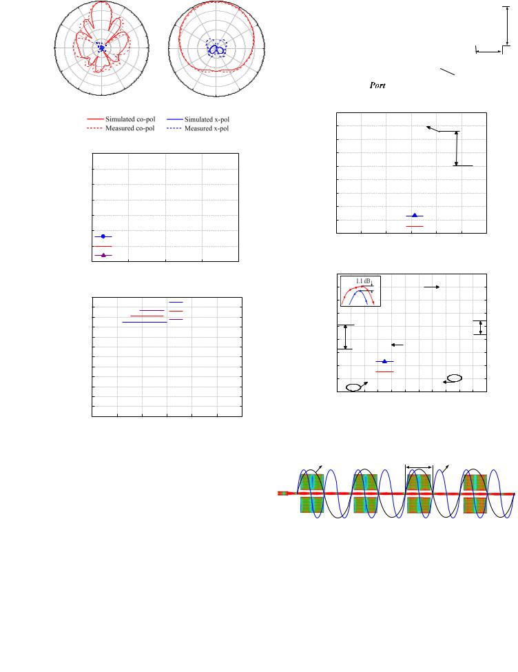
at 3.4 GHz. Again, good agreement is observed between them. The measured co-polarized field in the E-plane is at least 43 dB stronger than its corresponding cross-polarized counterpart. For the H-plane, the measured co-polarized field is 38 dB stronger than its corresponding cross-polarized counterpart. With reference to the measured front-to-back radio, it is more than 22 dB.
It is noted that the proposed method is also applicable when the number of the patches is increased within a certain range. Fig. 9 shows the simulated S11 and boresight gains of the single-band filtering array with four, eight and sixteen elements. As observed, the impedance bandwidth (|S11| < -10 dB) of the three arrays is 5 % (3.35-3.52 GHz). The realized gains within
5
Element 1 |
Element 2 |
Element 3 |
Element 4 |
W
L
 Power divider
Fig. 10. Configuration of the traditional array fed by 4-way power divider.
|
15 |
|
|
|
|
|
|
|
|
|
|
|
|
|
|
10 |
|
|
|
High-order mode |
|
|
|
|
|
||||
|
|
|
|
7.68 dBi |
|
|
|
|
|
|
||||
|
|
|
|
|
|
|
|
|
|
|
||||
(dBi) |
5 |
|
|
|
|
|
|
|
|
|
|
|
|
|
0 |
|
|
|
|
|
|
|
12.68 dB |
|
|
|
|||
gain |
|
|
|
|
|
|
|
|
|
|
|
|||
-5 |
|
|
|
|
|
|
|
|
|
|
|
|
|
|
|
|
|
|
|
|
|
|
|
|
|
|
|
|
|
Boresight |
-10 |
|
|
|
|
|
|
|
|
|
|
|
|
|
-20 |
|
|
|
|
|
|
|
|
|
|
|
|
|
|
|
-15 |
|
|
|
|
|
|
|
|
|
|
|
|
|
|
-25 |
|
|
|
|
|
|
|
Traditional array |
|
|
|||
|
3 GHz 3.7 GHz |
|
|
|
Proposed array |
|
|
|||||||
|
-302 |
|
|
|
|
|
||||||||
|
|
3 |
|
4 |
|
5 |
|
6 |
|
7 |
|
8 |
|
|
|
|
|
|
|
Frequency (GHz) |
|
|
|
|
|
||||
|
|
|
|
|
|
|
(a) |
|
|
|
|
|
|
|
|
15 |
|
|
|
|
|
|
|
Gain |
|
|
15 |
|
|
|
10 |
|
|
|
|
|
|
|
|
|
10 |
|
||
coefficientReflection(dB) |
|
|
|
|
|
|
|
|
|
|
|
|
||
5 |
|
|
|
|
|
|
|
|
|
|
|
5 |
gainBoresight(dBi) |
|
0 |
|
|
|
|
|
|
|
|
|
|
|
0 |
||
|
|
|
|
|
|
|
|
|
|
|
|
|
||
|
-5 |
|
|
|
|
|
|
|
|
|
5 dB |
-5 |
|
|
|
|
|
|
|
|
|
|
|
|
|
|
|
||
|
-10 |
9.5 dB |
S |
|
|
|
|
|
|
|
-10 |
|
||
|
|
|
|
|
|
|
|
|
|
|
||||
|
|
|
|
|
|
|
|
|
|
|
|
|
||
|
-15 |
|
|
|
11 |
|
|
|
|
|
|
|
-15 |
|
|
|
|
|
|
|
|
|
|
|
|
|
|
||
|
-20 |
|
|
|
Traditional array |
|
|
-20 |
|
|||||
|
|
|
|
Proposed array |
|
|
|
|||||||
|
-25 |
|
|
|
|
|
-25 |
|
||||||
|
|
Lower null |
Upper null |
|
|
|
||||||||
|
|
|
|
|
|
|
||||||||
|
-30 |
|
|
|
|
|
|
|
|
|
|
|
-30 |
|
|
2.9 |
3.0 |
3.1 |
3.2 |
3.3 |
3.4 |
3.5 |
3.6 |
3.7 |
3.8 |
3.9 |
4.0 |
|
|
|
|
|
|
|
Frequency (GHz) |
|
|
|
|
|
||||
(b)
Fig. 11. Performance comparison of the traditional array and proposed one (a) out-of-band, (b) in-band.
Fundamental |
L |
Second |
|
mode |
harmonic |
||
|
Fig. 12. Current distribution on the proposed array at the frequency 2 f0.
the operating band are 12.6 dBi, 15.6 dBi and 18.4 dBi. All the three arrays feature high frequency selectivity and out-of-band rejection levels. When the number of elements increases from four to eight and from eight to sixteen, the gain enhancement is 3 dB and 2.8 dB, respectively. This indicates that with less than sixteen elements, the proposed feeding scheme can be applied.
0018-926X (c) 2016 IEEE. Personal use is permitted, but republication/redistribution requires IEEE permission. See http://www.ieee.org/publications_standards/publications/rights/index.html for more information.

This article has been accepted for publication in a future issue of this journal, but has not been fully edited. Content may change prior to final publication. Citation information: DOI 10.1109/TAP.2017.2717046, IEEE Transactions on Antennas and Propagation
6
TABLE II
COMPARISON OF THE THREE PATCH ANTENNA ARRAYS
|
Element |
Filtering |
Gain |
Out-of-band |
Second |
|
|
suppression |
harmonic |
||||
|
numbers |
circuits |
(dBi) |
|||
|
level (dB) |
suppression |
||||
|
|
|
|
|||
|
|
|
|
|
|
|
Array in |
4 |
Fourth |
9.7 |
21.7 |
Yes |
|
[14] |
-order |
|||||
|
|
|
|
|||
|
|
|
|
|
|
|
Array in |
4 |
Third |
9.6 |
15.1 |
Yes |
|
[22] |
-order |
|||||
|
|
|
|
|||
|
|
|
|
|
|
|
Proposed |
4 |
None |
12.6 |
18.1 |
Yes |
|
array |
||||||
|
|
|
|
|
.
E. Comparison
To address the advantages of the proposed design, a traditional and a series-fed patch array are compared with the proposed single-band filtering array. The comparison results are presented in detail as follows.
1) Comparison with Traditional Patch Array
Fig. 10 shows the configuration of the traditional 4-element patch array fed by a 4-way power divider [33]. The length L and width W of the radiating patches are the same with that of the proposed antenna array. Also, the edge-to-edge distance between two elements is around 0.5 λg. As shown in Fig. 10, the traditional patch array occupies larger circuit size than the proposed filtering patch array because of the 4-way power divider.
Fig. 11(a) shows the simulated boresight gains of the two arrays over a wide frequency range from 2 to 8 GHz. Obviously, the proposed filtering patch array has wider stop-band with enhanced radiation suppression levels. Within the frequency bands of 2.0-3.0 GHz and 3.7-8.0 GHz, the gains of the proposed array are effectively suppressed to less than -5 dBi, resulting in more than 17.6 dB radiation rejection levels. Around the second harmonic frequencies, the antenna gains are significantly reduced by 12.68 dB as compared to the traditional patch array. This verifies the capability of harmonic suppression of the integrated design. Fig. 12 shows the current distribution of the proposed array at the frequency 2f0. As observed, out-of-phase currents are induced on the patches. This is because the electrical length of the patch is one wavelength at 2f0. The current at the midpoint of each coupling region is very weak, while the currents in the left and right half regions are out-of-phase, which is the same as case 2 as presented above in Part B. Therefore, the induced currents are out-of-phase, resulting in low realized gain at boresight direction.
With reference to the in-band performance, the simulated reflection coefficients and boresight gains within 2.9-4.0 GHz are presented in Fig. 11(b). The maximum in-band gains of the two arrays are 12.6 dBi and 11.5 dBi. The lower gain of the traditional patch array is due to the insertion loss introduced by the power divider. The simulated operating frequency range of the proposed filtering patch array with |S11| lower than -10 dB is 3.35-3.52 GHz (5%), while that of the traditional patch array is 3.4-3.46 GHz (1.7%). It’s also seen that the proposed filtering
|
Element 2 |
Element 3 |
Element 4 |
Element 1 |
|
||
|
|
|
L
(a)
Low-pass step- |
L-shaped |
impedance |
radiator |
network |
|
(b)
Fig. 13. Configuration of the series-fed antenna array (a) in [34]-[35], (b) in [36].
(dB) |
0 |
|
|
|
|
|
|
|
-5 |
|
|
|
|
|
|
|
|
coefficient |
|
|
|
|
|
|
|
|
-10 |
Resonant mode |
|
|
|
|
|||
|
|
|
|
|
||||
Reflection |
-15 |
|
|
|
|
|
|
|
-20 |
|
|
|
Proposed array |
|
|
||
|
|
|
|
|
|
|
|
|
|
-25 |
|
|
|
Series-fed array |
|
|
|
|
|
|
|
|
|
|
|
|
|
-30 |
|
|
|
|
|
|
|
|
2.0 |
2.5 |
3.0 |
3.5 |
4.0 |
4.5 |
5.0 |
|
|
|
|
|
Frequency (GHz) |
|
|
||
Fig. 14. Reflection coefficients of the two arrays.
antenna array exhibits sharper roll-off-rate because of the two radiation nulls generated near to the passband.
The proposed design is also compared to the two four-element patch arrays with filtering responses [14] and [22]. The comparison results are tabulated in Table II. The two arrays in [14] and [22] feature high out-of-band radiation rejection levels and wide stop-band. However, the gains of the two arrays are nearly 3 dB lower than that of the proposed work, which is due to the insertion losses introduced by the filtering feeding networks.
In sum, the proposed patch array features compact size, simple structure and high filtering performance without filtering circuits, which are highly demanded in wireless communications.
2) Comparison with Series-fed Antenna Array
The proposed design is compared to two series-fed antenna arrays in [34] [35] and [36]. As shown in Fig. 13(a), the array in [34] [35] consists of four rectangular patches with different width. The patches are fed by a microstrip line. The array in [36] consists four L-shaped radiators operating at 2.4 GHz and four low-pass step-impedance networks, as shown in Fig. 13(b).
0018-926X (c) 2016 IEEE. Personal use is permitted, but republication/redistribution requires IEEE permission. See http://www.ieee.org/publications_standards/publications/rights/index.html for more information.

This article has been accepted for publication in a future issue of this journal, but has not been fully edited. Content may change prior to final publication. Citation information: DOI 10.1109/TAP.2017.2717046, IEEE Transactions on Antennas and Propagation
TABLE III
COMPARISON OF THE THREE PATCH ANTENNA ARRAYS
|
Impedance |
Gain |
Out-of-band |
Out-of-band |
|
|
suppression |
resonant |
|||
|
bandwidth |
(dBi) |
|||
|
level (dB) |
modes |
|||
|
|
|
|||
Array in |
1.1% |
12.2 |
2.77 |
6 |
|
[34]-[35] |
|||||
|
|
|
|
||
|
|
|
|
|
|
Array in |
4% / 7.5% |
13.3/ |
9.5 |
4 |
|
[36] |
14.5 |
||||
|
|
|
|||
|
|
|
|
|
|
Proposed |
5% |
12.6 |
20.6 |
0 |
|
array |
|||||
|
|
|
|
||
|
|
|
|
|
|
|
|
|
|
|
These networks act as not only low-pass feeding networks for the L-shaped radiators but also function as radiators at 5.5 GHz.
The array in [34] [35] has been simulated and the simulation results are shown in Fig. 14. As observed, the operating frequency of the series-fed array is 3.4 GHz and the impedance bandwidth is 1.1%, which is narrower than 5% of the proposed array. It is worth noting that six out-of-band resonant modes at 2.66, 2.86, 3.10, 3.81, 4.04, 4.29 GHz are excited, indicating poor filtering performance. With reference to the array in [36], the results are listed in Table III. As indicated, the out-of-band radiation rejection level is around 9.5 dB and four undesired out-of-band resonant modes are excited. In contrast, the out-of-band radiation rejection level of the proposed filtering patch array is 20.6 dB, which is more than 10 dB higher than that of the two counterparts. Furthermore, within the out-of-band frequency ranges 1.0-2.9 GHz and 3.6-5.0 GHz, no extra resonant mode is generated and the return loss is less than 1 dB. These results indicate the proposed array performs high filtering performance compared to other two arrays.
III. DUAL-BAND FILTERING ANTENNA ARRAY
|
|
|
|
|
|
|
|
|
|
|
|
|
|
|
|
|
|
|
|
|
|
|
7 |
||||
|
|
|
|
|
|
L11 |
|
|
|
|
|
|
|
|
|
|
|
|
|
|
|
|
|||||
|
|
|
|
|
|
|
|
|
L22 |
|
|
|
|
|
|
|
|
|
|
|
|
|
|
|
|
||
|
|
Port |
|
|
|
|
|
W44 |
|
|
|
G11 |
|
|
|
|
|
||||||||||
W11 |
|
|
|
|
|
|
|
|
|
|
|
|
|
|
|
|
|
|
W22 |
||||||||
|
|
|
|
|
|
|
|
|
|
|
|
|
|
|
|
|
|
|
|
|
|
|
|
|
|||
|
|
|
|
|
|
|
|
|
|
|
|
|
|
|
|
|
|
|
|
|
|
|
|
|
|||
|
|
|
|
|
|
|
|
|
|
|
|
|
|
|
|
|
|
|
|
|
|
|
|
|
|
||
|
|
|
|
|
|
|
|
|
|
|
|
|
G22 |
|
|
|
|
|
|
|
|
|
|
|
|||
|
|
|
|
L33 |
|
|
|
|
|
|
L55 |
L66 |
|||||||||||||||
|
|
|
|
W33 |
|
|
|
|
|||||||||||||||||||
|
|
|
|
|
|
|
|
|
|
|
|
|
|
|
|
|
|
|
|
|
|
|
|
||||
|
|
|
|
|
|
|
|
|
|
|
|
|
|
|
|
|
|
|
|
|
|
|
|
|
|||
|
|
|
|
|
|
|
|
|
|
|
|
|
|
|
|
|
|
|
|
|
|
|
|
|
|
|
|
|
|
|
|
|
|
|
L44 |
|
|
|
|
|
|
|
|
|
|
|
|
|
|
|
|
||||
|
|
|
|
|
|
|
|
|
|
|
|
|
|
|
|
|
|
|
Feed line and patches |
Hsub |
|||||||
|
|
|
|
|
|
|
|
|
|
|
|
|
|
|
|
|
|
|
|
|
|
|
|||||
|
|
|
|
|
|
|
|
|
|
|
|
|
|
|
|
|
|
|
|
|
|
|
|
|
|
|
|
 Ground
GW1
GL1
Fig. 15. Configuration of the proposed dual-band filtering patch antenna array.
y
x
Fig. 16. Photograph of the dual-band filtering patch antenna array.
|
10 |
|
|
|
|
|
10 |
|
coefficientReflection(dB) |
5 |
|
|
|
Gain |
|
5 |
|
0 |
|
|
Measurement |
|
0 |
gainBoresight(dBi) |
||
-5 |
S |
|
|
-5 |
||||
|
11 |
|
|
|
|
|
||
|
-10 |
|
|
|
|
|
-10 |
|
|
-15 |
|
|
|
|
|
-15 |
|
|
-20 |
|
|
Simulation |
|
-20 |
|
|
|
|
|
|
|
|
|
||
|
-25 |
|
|
|
|
|
-25 |
|
|
-30 |
|
|
|
|
|
-30 |
|
|
2.0 |
2.5 |
3.0 |
3.5 |
4.0 |
4.5 |
5.0 |
|
|
|
|
Frequency (GHz) |
|
|
|
||
Besides the single-band filtering array, the proposed method can be also adopted to design a dual-band filtering array with simple structure and compact size, which is presented below.
A. Antenna Design
Fig. 15 shows the proposed dual-band filtering patch array. It consists of two 3-element sub-arrays operating at different frequencies (f1 and f2) and a feed line. They are fabricated on a substrate with the relative permittivity of 3.38 and thickness of 1.524 mm. The two 3-element sub-arrays are edge-coupled to the feed line and they are located on both sides of the feed line. The edge-to-edge distance of the elements in each sub-array is 0.5 λgi (λgi denotes the wavelength at fi in the substrate, i=1, 2).
The design guideline of this dual-band filtering patch array is summarized as follows.
1)Firstly, design two sub-arrays with operating frequencies f1 and f2. For each sub-array, set the initial dimensions of the patch as length L ≈ 0.4 λgi and width W ≈ 0.5 λgi. Set the edge-to-edge distance of the patches as 0.5 λgi.
2)Secondly, tune the length of the feed line and then observe the current distribution on it at the frequencies f1 and f2. Set the initial dimensions of the feed line as length Lfeed = 3.5λg1 = 4.5λg2. Select proper coupling regions as the same to case 1 for
the sub-array with operating frequency f1. Then place it on one
Fig. 17. Reflection coefficient and boresight gain of the proposed dual-band filtering patch antenna array.
TABLE IV
PARAMETERS OF THE DUAL-BAND FILTERING PATCH ARRAY
Length |
L11 |
L22 |
L33 |
L44 |
L55 |
L66 |
W11 |
|
|
|
|
|
|
|
|
Value (mm) |
23.4 |
27.6 |
21.6 |
29.4 |
37.6 |
38.7 |
3.52 |
|
|
|
|
|
|
|
|
|
|
|
|
|
|
|
|
Length |
W22 |
W33 |
W44 |
G1 |
G2 |
GW1 |
GL1 |
|
|
|
|
|
|
|
|
Value (mm) |
1.92 |
13.6 |
13.6 |
1.44 |
0.94 |
35 |
260 |
|
|
|
|
|
|
|
|
Length |
Hsub |
|
|
|
|
|
|
|
|
|
|
|
|
|
|
Value (mm) |
1.524 |
|
|
|
|
|
|
|
|
|
|
|
|
|
|
side of the feed line. After that, select proper coupling regions for the sub-array operating at f2 and place it on the other side of the feed line.
3) Finally, refine each parameter to optimize the design for obtaining good filtering performance.
B. Experiment
The dual-band filtering patch array is also fabricated and its prototype is shown in Fig. 16. The optimized parameters are presented in Table I V. The simulated and measured reflection
0018-926X (c) 2016 IEEE. Personal use is permitted, but republication/redistribution requires IEEE permission. See http://www.ieee.org/publications_standards/publications/rights/index.html for more information.

This article has been accepted for publication in a future issue of this journal, but has not been fully edited. Content may change prior to final publication. Citation information: DOI 10.1109/TAP.2017.2717046, IEEE Transactions on Antennas and Propagation
8
(a)
(b)
Fig. 18. Current distribution on the patch array at (a) 2.8 GHz and (b) 3.45 GHz
|
10 |
|
|
|
|
|
|
(dBi) |
5 |
|
|
|
|
17 dB |
|
-5 |
|
|
|
|
|
||
|
0 |
|
|
|
|
|
|
gain |
-10 |
|
|
|
|
|
|
|
|
|
|
|
|
|
|
Boresight |
-15 |
|
Low band sub-array |
|
|
||
-20 |
|
|
|
||||
|
|
|
|
|
|
|
|
|
-25 |
|
|
|
|
|
|
|
-30 |
|
|
|
|
|
|
|
-35 |
|
high band sub-array |
|
|
||
|
-40 |
|
|
|
|||
|
|
|
|
|
|
|
|
|
2.0 |
2.5 |
3.0 |
3.5 |
4.0 |
4.5 |
5.0 |
|
|
|
Frequency (GHz) |
|
|
||
Fig. 19. Boresight gains of the sub-arrays.
15 |
|
|
10 |
1:1.1 |
1:2.1 |
|
|
(dBi) |
0 |
|
|
|
|
|
|
|
|
|
|
|
5 |
|
|
|
|
|
|
|
|
|
|
gain |
|
|
|
|
|
0 dBi |
|
|
|
|
|
-5 |
|
|
|
|
|
|
|
|
|
|
|
|
|
|
|
|
|
|
|
|
|
|
|
Boresight |
-10 |
|
|
|
|
|
|
|
|
|
|
-25 |
|
|
|
|
|
|
|
|
|
|
|
|
-15 |
|
|
|
|
|
|
|
|
|
|
|
-20 |
|
|
|
|
|
|
|
|
|
|
|
-30 |
|
|
|
|
|
|
|
|
|
|
|
2.0 |
2.5 |
3.0 |
3.5 |
4.0 |
4.5 |
5.0 |
5.5 |
6.0 |
6.5 |
7.0 |
|
|
|
|
Frequency (GHz) |
|
|
|
||||
Fig. 20. Boresight gains of two dual-band patch array with different frequency ratios of the operating bands.
coefficient and boresight gain are illustrated in Fig. 17. Good agreement between the simulation and measurement is achieved. It can be seen that the center frequencies of the two operating bands are 2.8 and 3.45 GHz. The measured maximum gains are 10 and 9.9 dBi for the two bands. The out-of-band gains are less than -5 dBi, indicating around 15 dB out-of-band radiation rejection levels. It’s noted in Fig. 17 that only one resonance mode is observed within each band, whereas, for the single-band array, it’s seen in Fig. 6 that there are two resonance mods within its operating band. This is because the coupling between adjacent elements as well as that between the feedline and elements has impact on the resonance characteristic of the antenna array [31] [32]. For the dual-band array, the coupling between the feedline and patches are not as strong as that of the single-band array, resulting in only one resonance mode in each operating band.
To clarify the working mechanism of the proposed dual-band filtering array, Fig. 18 plots the current distribution at 2.8 and 3.45 GHz. It can be seen that when the array operates at 2.8
300
270
240
300
270
240
|
0 |
|
|
330 |
|
30 |
|
|
-10 |
|
|
|
-20 |
60 |
300 |
|
-30 |
||
|
|
|
|
|
-40 |
|
|
|
-50 |
90 270 |
|
|
|
||
|
|
120 |
240 |
210 |
|
150 |
|
|
180 |
|
|
x-z plane (E-plane)
|
|
(a) |
|
|
0 |
|
|
330 |
30 |
|
|
|
-10 |
|
|
|
-20 |
60 |
300 |
|
|
||
|
-30 |
|
|
|
-40 |
|
|
|
-50 |
90 |
270 |
|
|
||
|
|
120 |
240 |
210 |
150 |
|
|
|
180 |
|
|
x-z plane (E-plane) |
|
|
|
(b)
|
0 |
|
330 |
|
30 |
|
-10 |
|
|
-20 |
60 |
|
|
|
|
-30 |
|
|
-40 |
|
|
-50 |
90 |
|
|
|
|
|
120 |
210 |
|
150 |
|
180 |
|
y-z plane (H-plane)
|
0 |
|
330 |
30 |
|
|
-10 |
|
|
-20 |
60 |
|
|
|
|
-30 |
|
|
-40 |
|
|
-50 |
90 |
|
|
|
|
|
120 |
210 |
150 |
|
|
180 |
|
y-z plane (H-plane) |
|
|
Fig. 21. Radiation patterns of the dual-band filtering patch array at (a) 2.8 GHz,
(b) 3.45 GHz.
GHz, strong currents concentrate on the patches of the lower band sub-array. At 3.45 GHz, only the upper band sub-array is excited. Since one sub-array has little impact on the other one, the two sub-arrays can be independently designed and the passbands can be independently controlled. For further verification, the simulated boresight gains of the antenna with only one sub-array are illustrated in Fig. 19. As observed, both the two sub-arrays feature high filtering performance with out-of-band radiation rejection levels of more than 17 dB. This demonstrates that the two sub-arrays of the dual-band filtering patch array can be individually designed. As a result, the frequency ratio of the two operating bands can be controlled. To explore the high and low bounds of the frequency ratio, two dual-band antenna arrays with different frequency ratios are simulated. Fig. 20 plots the simulation results. As observed, the operating frequency of the upper-band sub-array can be tuned from 3.1 GHz to 5.7 GHz without affecting the operating frequency of the lower-band array. It’s also seen that when the operating frequency of upper-band sub-array is 3.1 GHz and 5.7 GHz, the out-of-band radiation rejection levels decrease to around 10 dB. Therefore, when the out-of-band radiation rejection level of this filtering patch array is required to be no less than 10 dB, the high and low bounds of frequency ratios are 1:2.1 and 1:1.1.
Fig. 21 plots the measured and simulated radiation patterns of the proposed antenna. Again, good agreement is observed between them. Low cross-polarization and low back radiation levels are obtained. At 2.8 and 3.45 GHz, the measured co-polarized fields in the E-plane are at least 21 dB and 24 dB
0018-926X (c) 2016 IEEE. Personal use is permitted, but republication/redistribution requires IEEE permission. See http://www.ieee.org/publications_standards/publications/rights/index.html for more information.
This article has been accepted for publication in a future issue of this journal, but has not been fully edited. Content may change prior to final publication. Citation information: DOI 10.1109/TAP.2017.2717046, IEEE Transactions on Antennas and Propagation
9
stronger than their corresponding cross-polarized counterparts, respectively. For the H-plane, the measured co-polarized fields are 30 dB and 32 dB stronger than their corresponding cross-polarized counterparts. With reference to the measured front-to-back radios, they are more than 17 dB and 20 dB for the lower and upper bands, respectively. It is worth mentioning that the E-plane radiation patterns are a bit asymmetric due to the asymmetric feed structure.
In sum, the proposed patch array obtains dual-band filtering performance without using extra filtering circuits. In addition, the center frequencies of the two operating passbands can be individually controlled, featuring high design freedom.
IV. CONCLUSION
In this paper, a novel feeding scheme for patch antenna arrays with singleand dual-band filtering performance has been proposed. Without using filtering circuits, the patch arrays exhibit high filtering performance by employing only a transmission line and radiating patches. Specific coupling regions have been characterized and then utilized to suppress out-of-band radiation without degrading in-band performance. Using this method, a single-band and a dual-band filtering patch arrays have been successfully designed and fabricated. Comparison with other designs has been conducted, showing the advantages of simple structure, compact size and enhanced out-of-band radiation suppression. Moreover, this design method can be applied to design multi-band filtering patch arrays by adding more sub-arrays along the feed line.
REFERENCES
[1]H. Chu, J.-X. Chen, S. Luo, and Y.-X. Guo, “A millimeter-wave filtering monopulse antenna array based on substrate integrated waveguide technology,” IEEE Trans. Antennas Propag., vol. 64, no. 1, pp. 316-321, Jan. 2016.
[2]H. Chu, C. Jin, J.-X. Chen, and Y.-X. Guo, “A 3-D millimeter-wave filtering antenna with high selectivity and low cross-polarization,” IEEE Trans. Antennas Propag., vol. 63, no. 5, pp. 2375-2380, May 2015.
[3]H. Tang, J.-X. Chen, H. Chu, G.-Q. Zhang, Y.-J. Yang, and Z.-H. Bao, “Integration design of filtering antenna with load-insensitive multilayer balun filter,” IEEE Trans. Antennas Propag., vol. 6, no. 9, pp. 1408-1416, Sep. 2016.
[4]M.-C. Tang, H. Wang, T.-W. Deng, and R.-W. Ziolkowski, “Compact planar ultra-wideband antennas with continuously tunable, independent band-notched filters,” IEEE Trans. Antennas Propag., vol. 64, no. 8, pp. 3292-3301, Aug. 2016.
[5]M. Barbuto, F. Trotta, F. Bilotti, and A. Toscano, “Horn antennas with integrated notch filters,” IEEE Trans. Antennas Propag., vol. 63, no. 2, pp. 781-785, Feb. 2015.
[6]P.-Y. Qin, F. Wei, and Y.-J. Guo, “A wideband-to-narrowband tunable antenna using a reconfigurable filter,” IEEE Trans. Antennas Propag., vol. 63, no. 5, pp. 2282-2285, May 2015.
[7]G. Q. Luo, W. Hong, H.-J. Tang, J.- X. Chen, X.-X. Yin, Z.- Q. Kuai, and
K.Wu, “Filtenna consisting of horn antenna and substrate integrated-waveguide cavity FSS,” IEEE Trans. Antennas Propag., vol. 55, no. 1, pp. 92–98, Jan. 2007.
[8]M. Barbuto, F. Trotta, F. Bilotti, and A. Toscano, “A combined bandpass filter and polarization transformer for horn antennas,” IEEE Antennas Wireless Propag. Lett., vol. 12, pp. 1065–1068, Sep. 2013.
[9]H. Zhou, S.-B. Qu, B.-Q. Lin, J.-F. Wang, H. Ma, Z. Xu, W.- D. Peng, and
P.Bai., “Filter-antenna consisting of conical FSS radome and monopole antenna,” IEEE Trans. Antennas Propag., vol. 60, no. 6, pp. 3040–3045, Jun. 2012.
[10]J. Zuo, X. Chen, G. Han, L. Li, and W. Zhang, “An integrated approach to RF antenna-filter co-design,” IEEE Antennas Wireless Propag. Lett., vol. 8, pp. 141–144, Jan. 2009.
[11]Y. Chen, W. Hong, Z. Kuai, and H. Wang, “Ku-band linearly polarized omnidirectional planar filtenna,” IEEE Antennas Wireless Propag. Lett., vol. 11, pp. 310–313, Mar. 2012.
[12]C.-X. Mao, S. Gao, Y. Wang, F. Qin, and Q.-X. Chu, “Multi-Mode resonator-fed dual polarized antenna array with enhanced bandwidth and selectivity,” IEEE Trans. Antennas Propag., vol. 63, no. 19, pp. 5492-5499, Oct. 2015.
[13]C.-X. Mao, S. Gao, Y. Wang, B. Sanz-Izquierdo, Z.-P. Wang, F. Qin, Q.-X. Chu, J.-Z. Li, W.-Gao, and J.-D. Xu, “Dual-band patch antenna with filtering performance and harmonic suppression,” IEEE Trans. Antennas Propag., vol. 64, no. 9, pp. 4074-4077, Jun. 2016.
[14]C.-X. Mao, S. Gao, Y. Wang, Z.-P. Wang, F. Qin, B.-S. Izquierdo, and Q.-X. Chu, “An integrated filtering antenna array with high selectivity and harmonic suppression,” IEEE Trans. Microw. Theory Techn., vol. 64, no. 6, pp. 1798-1805, Jun. 2016.
[15]C.-X. Mao, S. Gao, Y. Wang, F. Qin, and Q.-X. Chu, “Compact highly integrated planar duplex antenna for wireless communications,” IEEE Trans. Microw. Theory Techn., vol. 64, no. 7, pp. 2006-2013, Jun. 2016.
[16]Z.-H. Jaing, and D.-H. Werner, “A compact, wideband circularly polarized co-design filtering antenna and its application for wearable devices with low SAR,” IEEE Trans. Antennas Propag., vol. 63, no. 9, pp. 3808-3818, Sep. 2015.
[17]Z. H. Jiang, M. D. Gregory, and D. H.Werner, “Design and experimental investigation of a compact circularly polarized integrated filtering antenna for wearable biotelemetric devices,” IEEE Trans. Biomed. Circuits Syst., vol. 10, pp. 328–338, Feb. 2016.
[18]C.-Y. Hsieh, C.-H. Wu, and T.-G. Ma, “A compact dual-band filtering patch antenna using step impedance resonators,” IEEE Antennas Wireless Propag. Lett., vol. 14, pp. 1506-1509, May 2015.
[19]Y.-J. Lee, G.-W. Cao, and S.-J. Chung, “A compact dual-band filtering microstrip antenna with the same polarization planes,” in Proc. Asia-Pacific Microw. Conf., 2012, pp. 1178-1180.
[20]C.-T. Chuang and S.-J. Chung, “Synthesis and design of a new printed filtering antenna,” IEEE Trans. Antennas Propag., vol. 59, no. 3, pp.1036-1042, Mar. 2011.
[21]C.-T. Chuang and S.-J. Chung, “A compact printed filtering antenna using a ground-intruded coupled line resonator,” IEEE Trans. Antennas Propag., vol. 59, no. 10, pp. 3630-3637, Oct. 2011.
[22]C.-K. Lin, and S.-J. Chuang, “A filtering microstrip antenna array,” IEEE Trans. Microw. Theory Techn., vol.59, no. 11, pp. 2856-2863, Nov. 2011.
[23]L. Chen, and Y.-L. Luo, “Compact filtering antenna using CRLH resonator and defected ground structure,” Electron. Lett. vol. 50, pp. 1496-1498, Oct.2014.
[24]P.-C. Wu, L. Chen and Y.-L. Luo, “Miniaturised wideband filtering antenna by employing CRLH-TL and simplified feeding structure,” Electron. Lett. vol.51, pp. 548-550, Apr.2015.
[25]X.-Y. Zhang, Y. Zhang, Y.-M. Pan, and W. Duan, “Low-profile dual-band filtering patch antenna and its application in LTE MIMO system ,” IEEE Trans. Antennas Propag., vol. 65, no. 1, pp. 103-113, Jan. 2017.
[26]S.-W. Wong, T.-G. Huang, C.-X. Mao, Z.-N. Chen, and Q.-X. Chu, “Planar filtering ultra-wideband (UWB) antenna with shorting pins,” IEEE Trans. Antennas Propag., vol. 61, no. 2, pp. 948-953, Feb. 2013.
[27]X.-Y. Zhang, W. Duan, and Y.-M. Pan, “High-gain filtering patch antenna without extra circuit,” IEEE Trans. Antennas Propag., vol. 63, no. 12, pp. 5883-5888, Dec. 2015.
[28]Y. Zhang, X.-Y. Zhang, L.-H. Ye, and Y.-M. Pan, “Dual-band base-station array using filtering antenna elements for mutual coupling suppression,” IEEE Trans. Antennas Propag., vol. 64, no. 8, pp. 3423-3430, Aug. 2016.
[29]Y.-M. Pan, P.-F. Hu, X.-Y. Zhang, and S.-Y. Zheng, “A low-profile high-gain and wideband filtering antenna with metasurface,” IEEE Trans. Antennas Propag., vol. 64, no. 5, pp. 2010-2016, May 2016.
[30]J.-N. Wu, Z.-Q. Zhao, Z.-P. Nie, and Q.-H. Liu, “A printed unidirectional antenna with improved upper band-edge selectivity using a parasitic loop,” IEEE Trans. Antennas Propag., vol.63, no. 4, pp. 1832-1837, Apr. 2015.
[31]X. Y. Zhang, C. H. Chan, Q. Xue, and B. J. Hu, “RF tunable bandstop filters with constant bandwidth based on a doublet configuration,” IEEE Trans. Ind. Electron., vol. 59, no. 2, pp. 1257–1265, Feb. 2012.
[32]F. Huang, “Dual-band superconducting spiral filters including narrow bandstop notches,” IEEE Trans. Microw. Theory Tech., vol. 57, no. 5, pp. 1188–1195, May 2009.
[33]C. A. Balanis, Antenna Theory—Analysis and Design, 3rd ed. New York, NY, USA: Wiley, 2005.
0018-926X (c) 2016 IEEE. Personal use is permitted, but republication/redistribution requires IEEE permission. See http://www.ieee.org/publications_standards/publications/rights/index.html for more information.

This article has been accepted for publication in a future issue of this journal, but has not been fully edited. Content may change prior to final publication. Citation information: DOI 10.1109/TAP.2017.2717046, IEEE Transactions on Antennas and Propagation
10
[34]T. Yuan, N. Yuan, and L.-W. Li, “A novel series-fed taper antenna array design,” IEEE Antennas Wireless Propag. Lett., vol. 7, pp. 362–365, Jul. 2008.
[35]S. Sengupta, D. R. Jackson, and S. Long “A method for analyzing a linear series-fed rectangular microstrip antenna array,” IEEE Trans. Antennas Propag., vol.63, no. 8, pp. 3731-3736, Jul. 2015.
[36]W.-K. Toh, X.-M. Qing, and Z.-N. Chen, “A planar dual-band antenna array,” IEEE Trans. Antennas Propag., vol. 59, no. 3, pp. 833–838, Mar. 2011.
Yao Zhang was born in Hubei, China. He received the B.S. degree in electronics and information engineering from Xi’an University of Science and Technology, Xi’an, China, in 2013. He was a researcher with the City University of Hong Kong Shenzhen Research Institute from May 2014 to September 2014. He is now working toward the Ph.D. degree at School of Electronic and Information Engineering, South China University of Technology, Guangzhou, China. His current research interests
include microwave circuits, massive MIMO antennas and integration designs of filter and antenna.
Mr. Zhang was a recipient of the Best Student Paper Award at the IEEE 5th Asia-Pacific Conference on Antenna and Propagation (APCAP). He was also the recipient of the National Scholarship for Graduate Students in 2015 and 2016. He also serves as a reviewer of several international journals such as IEEE Transactions on Antennas and Propagation and IET Electronics Letters.
Xiu Yin Zhang (S’07-M’10- SM’12) received the B.
S. degree in communication engineering from Chongqing University of Posts and Telecommunications, Chongqing, China, in 2001, the M.S. degree in electronic engineering from South China University of Technology, Guangzhou, China, in 2006, and the PhD degree in electronic engineering from City University of Hong Kong, Kowloon, Hong Kong, in 2009.
From 2001 to 2003, he was with ZTE Corporation, Shenzhen, China. From 2006 to 2007, he was a Research Assistant with the City University of Hong Kong, where he was a Research Fellow from 2009 to 2010. He is currently a full professor with the School of Electronic and Information Engineering, South China University of Technology. He also serves the deputy director of Guangdong Provincial Engineering Research Center of Antennas and RF techniques and the vice director of the Engineering Research Center for Short-Distance Wireless Communications and Network, Ministry of Education. He has authored or coauthored more than 80 internationally referred journal papers including more than 60 IEEE journal papers and approximately 50 conference papers. His research interests include microwave circuits and sub-systems, antennas and arrays and wireless power transfer.
Dr. Zhang was a recipient of the Young Scholar of the Changjiang Scholars Program of Chinese Ministry of Education, the Top-Notch Young Professionals of the National Program of China, the National Science Foundation for Outstanding Young Scholars of China, and the Scientific and Technological Award (First Honor) of Guangdong Province. He was the Supervisor of several conference Best Paper Award recipients. He has served as a Technical Program Committee (TPC) Chair/member and a session Organizer/Chair for a number of conferences. He is an Associate Editor for IEEE ACCESS. He has been a regular Reviewer of several international journals including for seven IEEE TRANSACTIONS. He is a Fellow of the Institution of Engineering and Technology (IET).
Yong Mei Pan (M’11) was born in Huangshan,
Anhui Province, China. She received the B.Sc. and Ph.D. degrees in electrical engineering from the University of Science and Technology of China, Hefei, China, in 2004 and 2009, respectively. From 2009 to 2012, she was a Research Fellow with the Department of Electronic Engineering, City University of Hong Kong, Kowloon Tong, Hong Kong. In 2013, she joined the School of Electronic and Information Engineering, South China University
of Technology (SCUT), Guangzhou, China, as an Associate Professor.
Currently, she is a Professor with SCUT. Her research interests include dielectric resonator antennas, leaky wave antennas, metasurface antennas, and filtering antennas. Prof. Pan is now an Associate Editor of the IEEE Transactions on Antennas and Propagation.
0018-926X (c) 2016 IEEE. Personal use is permitted, but republication/redistribution requires IEEE permission. See http://www.ieee.org/publications_standards/publications/rights/index.html for more information.