

This article was downloaded by: [UOV University of Oviedo] On: 30 October 2014, At: 08:10
Publisher: Taylor & Francis
Informa Ltd Registered in England and Wales Registered Number: 1072954 Registered office: Mortimer House, 37-41 Mortimer Street, London W1T 3JH, UK
Journal of Electromagnetic Waves and Applications
Publication details, including instructions for authors and subscription information: http://www.tandfonline.com/loi/tewa20
Experimental comparison of waveguide filters at W-band implemented by different machining processes and split-block
Carlos A. Leal-Sevillanoa, José R. Montejo-Garaia, Jorge A. RuizCruzb & Jesús M. Rebollara
aDepartamento de Electromagnetismo y Teoría de Circuitos, Escuela Técnica Superior de Ingenieros de Telecomunicación, Universidad Politécnica de Madrid, Avenida Complutense 30, Madrid 28040, Spain
bEscuela Politécnica Superior, Universidad Autónoma de Madrid, C/Francisco Tomas y Valiente 11, Madrid 28049, Spain Published online: 23 Oct 2013.
To cite this article: Carlos A. Leal-Sevillano, José R. Montejo-Garai, Jorge A. Ruiz-Cruz & Jesús M. Rebollar (2013) Experimental comparison of waveguide filters at W-band implemented by different machining processes and split-block, Journal of Electromagnetic Waves and Applications, 27:18, 2390-2394, DOI: 10.1080/09205071.2013.851011
To link to this article: http://dx.doi.org/10.1080/09205071.2013.851011
PLEASE SCROLL DOWN FOR ARTICLE
Taylor & Francis makes every effort to ensure the accuracy of all the information (the “Content”) contained in the publications on our platform. However, Taylor & Francis, our agents, and our licensors make no representations or warranties whatsoever as to the accuracy, completeness, or suitability for any purpose of the Content. Any opinions and views expressed in this publication are the opinions and views of the authors, and are not the views of or endorsed by Taylor & Francis. The accuracy of the Content should not be relied upon and should be independently verified with primary sources of information. Taylor and Francis shall not be liable for any losses, actions, claims, proceedings, demands, costs, expenses, damages, and other liabilities whatsoever or
howsoever caused arising directly or indirectly in connection with, in relation to or arising out of the use of the Content.

This article may be used for research, teaching, and private study purposes. Any substantial or systematic reproduction, redistribution, reselling, loan, sub-licensing, systematic supply, or distribution in any form to anyone is expressly forbidden. Terms & Conditions of access and use can be found at http://www.tandfonline.com/page/terms- and-conditions
Downloaded by [UOV University of Oviedo] at 08:10 30 October 2014

Downloaded by [UOV University of Oviedo] at 08:10 30 October 2014
Journal of Electromagnetic Waves and Applications, 2013
Vol. 27, No. 18, 2390–2394, http://dx.doi.org/10.1080/09205071.2013.851011
Experimental comparison of waveguide filters at W-band implemented by different machining processes and split-block
Carlos A. Leal-Sevillanoa*, José R. Montejo-Garaia, Jorge A. Ruiz-Cruzb and
Jesús M. Rebollara
aDepartamento de Electromagnetismo y Teoría de Circuitos, Escuela Técnica Superior de Ingenieros de Telecomunicación, Universidad Politécnica de Madrid, Avenida Complutense 30, Madrid 28040, Spain; bEscuela Politécnica Superior, Universidad Autónoma de Madrid, C/Francisco Tomas y Valiente 11, Madrid 28049, Spain
(Received 8 May 2013; accepted 28 September 2013)
The aim of this work is to explore different machining processes and different split-block, getting important experimental information for the design of passive waveguide components at W-band. To this end, two all-pole response filters are machined by different techniques: electro-discharge and milling, and split-block: H-plane and E-plane. Some interesting results, obtained in the design, fabrication, and measure of waveguide filters at W-band, such as tolerances of the different processes and level of insertion loss, are reported.
Keywords: W-band; waveguide; filter; low loss
1. Introduction
Different systems at W-band (75–110 GHz) have been proposed lately, such as radio-astronomy, weather, and image radar and recently communication equipments. At these high frequency the ohmic losses are very high, making the waveguide technology the preferred alternative for passive components. Among passive circuits, filters are essential devices for the performance of the entire system. They are used for reducing or selecting the received noise, eliminating spurious signals generated by non-linear devices or efficiently controlling the radio spectrum. In the case of radio-astronomy and radar applications, when the performance of these systems can be improved, the availability of waveguide filters is desired. For the case of the recent communication applications at this band the efficient control of the spectrum is mandatory.
Some waveguide filters and multiplexers were designed at W-band in the past.[1,2] All these previous designs were based on the classical E-plane filters. This is because the metal insert can be machined accurately by laser ablation making this kind of topologies the only alternative. Nevertheless, this kind of filters presents some drawback, in particular for relatively wide band the thickness of the first metal insert is too thin, leading to possible errors during the manufacture.
In the recent years, different designs were presented at this band using both, classical machining techniques [3] and new micromachining processes.[4] In spite of all these designs, it is still a challenge to fulfil stringent specifications at these high frequencies.
*Corresponding author. Email: caleal@etc.upm.es
© 2013 Taylor & Francis

Downloaded by [UOV University of Oviedo] at 08:10 30 October 2014
Journal of Electromagnetic Waves and Applications |
2391 |
2. Filter design and fabrication |
|
In order to gain experience in the design and fabrication process |
for waveguide |
filters at W-band, a fourth order all-pole filter was designed firstly. An H-plane topology was selected for an ease machining. The design is based on four in-line rectangular waveguide resonant cavities, using the TE101 resonant mode, coupled by symmetric inductive irises. The classical circuit synthesis is carried out as explained, for example in [5]. The final full-wave optimization was carried out by means of the Mode-Matching Technique (MMT). Since the filter has an H-plane topology (no height variation) and two-fold symmetry, only the TEm0 (m odd) modes are generated in the structure, leading to high-rate convergence of the MMT. The filter design is centered at 100 GHz with a 5% fractional bandwidth and a
minimum level |
of return loss in the band-pass of 25 dB. The input/output interface |
|||
corresponds to |
the standard |
WR-10 (2.54 × 1.27 mm). |
Moreover, thick |
irises of |
0.5 mm thickness were used |
in the design in order |
to avoid possible |
problems |
|
during the machining process. |
|
|
|
|
Two different prototypes of the fourth-order all-pole filter were fabricated. It is well known that the optimum split-block alternative is in the E-plane since no surface currents of the fundamental mode are interrupted. Nevertheless, if a good electrical contact in the H-plane split-block is guaranteed, some advantages such as lower cost and higher aspect ratio on the waveguide cross-section can be gained. These two possibilities are investigated experimentally.
The first filter was fabricated in brass by an electro-discharge process and H-plane split-block, Figure 1(a). Different mandrels were manufactured for implementing the different shapes of the filter, cavities, and irises, see Figure 1(c). An electro-discharge is generated between the mandrel and the piece to be manufactured. In that way, the
Figure 1. Fabricated filters. (a) electro-discharge and H-plane split-block. (b) milling and E-plane split-block. (c) metallic mandrels used for the electro-discharge process.

2392 |
C.A. Leal-Sevillano et al. |
Downloaded by [UOV University of Oviedo] at 08:10 30 October 2014
Figure 2. All-pole filter machined by electro-discharge and H-plane split-block.
metallic mandrels are introduced little by little drilling the piece. In Figure 2, the comparison between simulations and measurements is shown. The second filter was fabricated in brass by a milling process and E-plane split-block, Figure 1(b). The simulated and measured responses are shown in Figure 3.
3. Results and discussion
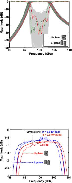
In Figures 2 and 3, the comparison between simulations and measurements for the filter implemented by electro-discharge and H-plane split-block and implemented by milling and E-plane split-block, respectively, are shown. In the first case, (electro-discharge and H-plane) a frequency shift of 200 MHz and 20 dB of minimum return loss level is observed, while for the second case (milling and E-plane) 500 MHz frequency shift and 25 dB of minimum return loss is obtained.
Figure 3. All-pole filter machined by milling and E-plane split-block.
Journal of Electromagnetic Waves and Applications |
2393 |
Downloaded by [UOV University of Oviedo] at 08:10 30 October 2014
Figure 4. Sensitivity analysis with ±10 μm, ideal conductors are used in the full-wave simulations.
Comparing both processes, on the one hand, the electro-discharge process used for the first filter needs additional implements leading to a higher manufacturing time. On the other hand, the H-plane split-block only needs to machine one of the pieces, which is an important advantage in terms of cost and time. In terms of the accuracy, both processes are similar, slightly better the electro-discharge with a frequency shift to 200 MHz against 500 MHz with milling. A sensitivity analysis was carried out to determinate the fabrication tolerance. All the dimensions of the filter were modified randomly by adding to each of the nominal values an independent uniform distribution between ±10 μm. A total of 300 simulations, without including losses, were carried out for the sensitivity analysis. The results are shown in Figure 4. As can be seen, the fabricated dimensions are within a tolerance of ±10 μm, completely explaining both, the frequency shift and the degradation in the return loss.
Figure 5. Insertion loss comparison.