

диафрагмированные волноводные фильтры / cee86372-e44d-4ce5-a255-1df259b0ba70
.pdfFigure 9 Photograph of the fabricated fourth-order dual-band BPF. [Color figure can be viewed in the online issue, which is available at www.interscience.wiley.com]
graph of the fabricated BPF circuit, which occupies an area of only 9.55 7.2 mm2 on the printed circuit board.
5.2. The Fourth-Order Butterworth BPF
Figure 8 shows the simulated results of the fourth-order Butterworth filter. The filter is designed with 8% for the 2.45 GHz band and 6% for the 5.25 GHz bands. The fractional bandwidths have been purposely set different from those of the above second-order BPF to demonstrate the flexibility of the proposed BPF design. The element values of the low-pass filter prototype are g0 g5 1, g1 g4 0.7654, and g2 g3 1.8478. The coupling coefficients obtained are M1,2 M3,4 0.067 and M2,3
0.043 at 2.45 GHz, and M1,2 M3,4 0.05 and M2,3 0.032 at 5.25 GHz. These coupling coefficients give rise to d 0.5 mm,
u 0 mm, e 0.7 mm, and v 3.2 mm, according to Figure 4 and the omitted coupling-coefficient curves for the PCL configuration. Moreover, the filter specifications yield Qe1 9.57 and Qe212.76, from which the optimized length of t 2.4 mm can be obtained after fine tuning in simulation. The measured fractional bandwidths (minimum insertion losses) for the 2.45 and 5.25 GHz bands are 7.14% (2.43 dB) and 5.14% (2.7 dB), respectively, which only slightly deviate from the simulated data of 8.38% (1.84 dB) and 5.8% (2.678 dB). The measured third passband center frequency around 9.85 GHz, like that of the above second-order BPF, is also very close to the one predicted in Section 2. The photograph of the fabricated fourth-order BPF is shown in Figure 9, whose circuit measures only 19.7 11 mm2.
6. CONCLUSION
In this article, the compact dual-band microstrip BPFs designed using U-shaped /4 SIRs have been proposed for the 2.45 and 5.25 GHz WLAN applications. Sample second-order and fourth-order dual-band BPFs have been designed and implemented, with a circuit size of only 9.55 7.2 mm2 and 19.7 11 mm2, respectively. Their first spurious passbands (around 10 and 9.85 GHz) were found to be very far away from the second passband. The transmission zero produced by the APCL sections of the filter has been purposely located between the two desired passbands to achieve good stopband rejection. The measured data showed that the fabricated BPFs not only have satisfactory response, but also have good agreement with the simulated results.
ACKNOWLEDGMENT
This work was supported by the National Science Council of the Republic of China (on Taiwan) under Grant NSC 95–2221-E-018 – 006.
REFERENCES
1.L.-L. Lu, H.-H. Hsieh, and Y.-S. Wang, A compact 2.4/5.2-GHz CMOS dual-band low-noise amplifier, IEEE Microwave Wireless Compon Lett 15 (2005), 685– 687.
2.H. Miyake, S. Kitazawa, T. Ishizaki, T. Yamada, and Y. Nagatomi, A miniaturized monolithic dual band filter using ceramic lamination technique for dual mode portable telephones, IEEE MTT-S Int Microwave Symp Dig WE3F-10 (1997), 789 –792.
3.L.C. Tsai and C.W. Hsue, Dual-band bandpass filters using equal-length coupled-serial-shunted lines and Z-transform technique, IEEE Trans Microwave Theory Tech 52 (2004), 1111–1117.
4.H.M. Lee, C.R. Chen, C.C. Tsai, and C.M. Tsai, Dual-band coupling and feed structure for microstrip filter design, IEEE MTT-S Int Microwave Symp Dig THIF-36 (2004), 1971–1974.
5.J.-T. Kuo, T.-H. Yeh, and C.-C. Yeh, Design of microstrip bandpass filters with a dual-passband response, IEEE Trans Microwave Theory Tech 53 (2005), 1331–1337.
6.M. Makimoto and S. Yamashita, Bandpass filters using parallel coupled stripline stepped impedance resonators, IEEE Trans Microwave Theory Tech MTT-28 (1980), 1413–1417.
7.K.U-yen, E.J. Wollack, T.A. Doiron, J. Papapolymerou, and J. Laskar, A planar bandpass filter design with wide stopband using double splitend stepped-impedance resonators, IEEE Trans Microwave Theory Tech 54 (2006), 1237–1244.
8.J.-S. Hong and M.J. Lancaster, Microstrip filters for RF/microwave applications, Wiley, New York, 2001.
9.C.-M. Tasi, S.-Y. Lee, and H.-M. Lee, Transmission-line filters with capacitively loaded coupled lines, IEEE Trans Microwave Theory Tech 51 (2003), 1517–1524.
© 2006 Wiley Periodicals, Inc.
SUBSTRATE INTEGRATED WAVEGUIDE HORN ANTENNA WITH DIELECTRIC LENS
Wenquan Che,1 Bing Fu,1 Ping Yao,1 and Y. L. Chow2
1 Department of Electrical Engineering, Nanjing University of Science and Technology, 210094 Nanjing, China
2 Department of Electrical and Computer Engineering, University of Waterloo, Waterloo,
ON, Canada N2L3G1
Received 18 May 2006
ABSTRACT: A novel compact H-plane horn antenna constructed is proposed for substrate integrated rectangular waveguide with r 10.2. It has a dielectric arc lens for better directivity and a simple microstrip transition as feed. The horn, the lens, and the transition share the same substrate. The measured gain of this antenna is about 9 dB; the bandwidth, at 10 dB return loss, is over 12%, and the antenna size is
39.175 14 2 mm3. The frequency band is 25.5–28.5 GHz. © 2006 Wiley Periodicals, Inc. Microwave Opt Technol Lett 49: 168 –170, 2007; Published online in Wiley InterScience (www.interscience.wiley. com). DOI 10.1002/mop.22086
Key words: SIRW; horn antenna; dielectric arc lens; radiation pattern; return loss
1. INTRODUCTION
The rectangular waveguide structure, as we know, has advantages over other planar transmission lines for millimeter band applications, but its implementation in planar form seems to be difficult due to its 3D geometry. This difficulty was resolved a few years ago by the proposed substrate-integrated rectangular waveguide
168 |
MICROWAVE AND OPTICAL TECHNOLOGY LETTERS / Vol. 49, No. 1, January 2007 |
DOI 10.1002/mop |

(SIRW) [1–3]. It is an artificial waveguide structure that is fabricated in planar substrate with periodic metallic cylinders, and preserves much of the properties of a conventional rectangular waveguide (RWG). Substrate integrated waveguides have clear advantages over RWG including low cost, simple integration with planar devices, and a significant size reduction [4 – 6].
The rectangular waveguide horn antennas have found many applications due to their excellent radiation properties such as symmetry patterns, high gain, very wide bandwidth, and easy fabrication. Similar to the RWG above, due to the 3D nature and especially the horn size, the horns are difficult to integrate with planar circuits and system; this has limited their use to high performance satellite communications and radar applications.
We now propose an H-plane horn antenna that integrates easily into the planar SIRW to take full advantages of the latter. A dielectric arc lens is conveniently added to improve the directivity of the antenna. To continue the convenience, a simple transition to microstrip line is designed. The horn antenna, the microstrip transition, and the arc lens, integrated on a single substrate, result in a very compact integrated planar antenna.
2. DESIGN CONSIDERATIONS
2.1. Substrate-Integrated Rectangular Waveguide
The simulated model of the antenna is illustrated in Figure 1. Behind the flaring horn is the dielectric-filled rectangular waveguide (SIRW) constructed in the substrate. The significant characteristic of this waveguide is that the size is reduced in a factor of r 1/2. Following the design rules in Ref.1–3, the parameters are chosen as: SIRW width W4 7.112 mm, length L4 3.4 mm, cylinder radius r 0.4 mm, cylinder separation p 1 mm, substrate thickness h 2 mm, the width of the horn W1 14 mm, the dielectric constant r 10.2. The centre frequency is f0 27 GHZ.
2.2. Horn Section and the Arc Lens
Following the procedure for a conventional horn antenna [7], the flare angle of the horn is chosen as 10°, the length of the horn section L 17.775 mm. Based on the operation principle of the optical focus [8], an arc lens is placed before the radiation plane to improve the directivity of the horn antenna. We may note that the arc lens shares the same substrate with the horn antenna, the bottom ground plane of the horn stops at the opening of the horn before the lens like the top plate, the top and bottom plates are identical in shape.
2.3. Microstrip Transition
A computer-optimized tapered-transition from 50 microstrip feed line has been designed to provide a low-loss transition to the SIRW on the same substrate. As shown in Figure 1, the width of the microstrip line W2 3.8 mm, length L2 2 mm. The taper
TABLE 1 The Relation Between the Height H of the Dielectric Arc Lens and the E-Plane Beamwidth
H (mm) |
HPBW (°) |
|
|
0 |
160 |
1 |
150 |
2 |
140 |
3 |
135 |
4 |
90 |
5 |
80 |
6 |
75 |
7 |
68 |
|
|
Figure 1 The geometry of the SIRW horn antenna. W1 14 mm, W2 3.8 mm, W3 5.32 mm, L1 33.175 mm, L2 2 mm, L3 10 mm, L43.4 mm, H 6 mm, R 7.175 mm, 10°. The dielectric constant of the substrate r 10.2, thickness h 2 mm. [Color figure can be viewed in the online issue, which is available at www.interscience.wiley.com]
transition length L3 10 mm, the larger width of the transition W35.32 mm. The overall dimensions of the horn antenna are 39.175 14 2 mm3.
3. NUMERICAL AND EXPERIMENTAL RESULTS
The relation between the H-plane beamwidth (HPBW) and the arc height has been investigated numerically by HFSS and listed in Table 1. As we can see, the beamwidth of the radiation pattern is dependent on the arc height of the dielectric lens, i.e., stronger arc height results in narrower beam. We may note that, the arc height cannot exceed half of the horn width, beyond which the dielectric lens is not a normal arc and would result in the deterioration of the radiation pattern. For our hardware experiment, we have chosen the arc radius R 7.175 mm, the arc height H 6 mm.
An experimental prototype of the antenna was fabricated as shown in Figure 2. The simulated and measured H-plane and E-plane radiation patterns are illustrated in Figures 3(a) and 3(b) at 27 GHz, in the middle of the SIRW passband. The measured gain is about 9 dB, close to the simulation result, and the front-to-back ratio is about 15 dB.
The beamwidths, H and E planes for both simulated and measured, are quite similar, at about 60°. The E plane pattern has high sidelobes; this is expected in view of the thinness of the substrate at h 2 mm. Evidently, the sidelobes would be reduced if the substrate thickness h is increased. In addition, the roughness of the dielectric lens of the fabricated prototype may do a little contribution to the sidelobes.
Figure 2 The fabricated prototype of the SIW horn antenna with dielectric lens. [Color figure can be viewed in the online issue, which is available at www.interscience.wiley.com]
DOI 10.1002/mop |
MICROWAVE AND OPTICAL TECHNOLOGY LETTERS / Vol. 49, No. 1, January 2007 |
169 |
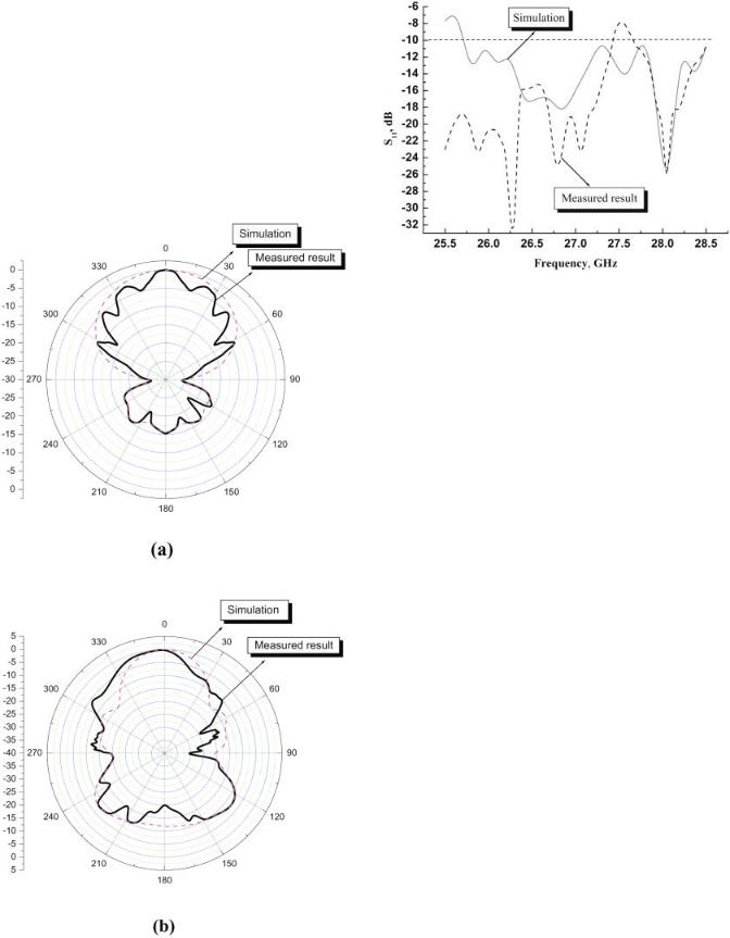
As shown in Figure 4, a bandwidth of 12% is measured for the return loss S11 at the 10 dB limits. The measured return loss is better than the simulation; however, it is a little worse around 27.5 GHz. This probably owes to the fabrication inaccuracies of the dielectric arc and the SIRW horn antenna in the substrate.
4. CONCLUSION
This letter designs a new H-plane SIRW horn antenna together with a dielectric lens for improving the directivity of the antenna. The design allows the design of a completely integrated planar platform of horn antenna and its feeding structure on the same substrate without any mechanical assembly or tuning. The mea-
Figure 3 The measured and simulated radiation patterns of the SIRW horn antenna (f0 27 GHz). (a) E-plane, (b) H-plane. [Color figure can be viewed in the online issue, which is available at www.interscience. wiley.com]
Figure 4 The measured and simulated S11 of the SIRW horn antenna, the arc height H 6 mm
sured results agree with the HFSS simulated ones for our fabricated sample of the integrated antenna. However, the measured bandwidth (return loss) is slightly narrower than the simulation, probably because of fabrication inaccuracy. With its compact integration and small size, this new scheme is well suited for antenna design at microwave and millimeter-wave frequencies.
ACKNOWLEDGMENTS
The authors express their gratitude for the financial support of National Science Foundation of China under Grant 60471025, Natural Science Foundation of Jiangsu Province under Grant BK2004135.
REFERENCES
1.J. Hirokawa and M. Ando, Single-layer feed waveguide consisting of posts for plane TEM wave excitation in parallel plates, IEEE Trans Antennas Propag 46 (1998), 625– 630.
2.D. Deslandes and K. Wu, Integrated microstrip and rectangular waveguide in planar form, IEEE Microwave Wireless Compon Lett 11 (2001), 68 –70.
3.W. Che, K. Deng, and Y.L. Chow, Equivalence between waveguides with side walls of cylinders (SIRW) and of regular solid sheets, in APMC2005 Proceedings, China, December 2005, Vol. 2, pp. 768 –770.
4.W. D’Orazio, K. Wu, and J. Helszajn, A substrate integrated waveguide degree-2 circulator, IEEE Microwave Wireless Compon Lett 14 (2004), 207–209.
5.D. Deslandes and K. Wu, Substrate integrated waveguide leaky-wave antenna: Concept and design considerations, in APMC2005 Proceedings, China, December 2005, Vol. 1, pp. 346 –349.
6.W. Che, K. Deng, E.K.N. Yung, and K. Wu, H-plane 3-dB hybrid ring of high isolation in substrate-integrated rectangular waveguide (SIRW), Microwave Opt Technol Lett 47 (2006), 502–505.
7.K. Nagasawa and L. Matsuzuka, Radiation field consideration of biconical horn antenna with different flare angles, IEEE Trans Antennas Propag 36 (1988), 1306 –1310.
8.M. Born and E. Wolf, Principles of optics, 6th ed., Pergamon, UK, 1980.
© 2006 Wiley Periodicals, Inc.
170 |
MICROWAVE AND OPTICAL TECHNOLOGY LETTERS / Vol. 49, No. 1, January 2007 |
DOI 10.1002/mop |