

диафрагмированные волноводные фильтры / db61eb9f-1c68-4298-9fba-d2f18ed5fd93
.pdfProceedings of the 45th European Microwave Conference
Design of a Surface Mounted Waveguide Filter in Substrate Integrated Waveguide Technology
J. Schorer1, J. Bornemann1 and Uwe Rosenberg2
1 Department of Electrical and Computer Engineering, University of Victoria, Victoria B.C., Canada
2 Mician Global Engineering GbR, Bremen, Germany
Abstract— In this paper, a novel combination of substrate integrated waveguide (SIW) and surface mounted waveguide (SMW) filter is presented for the purpose of reducing losses in SIW technology. The waveguide filter is comprised of five directly coupled resonators. Since the apertures in the top metallization of the SIW act as input/output inverters, no extra transitions are required to interface the two technologies. The SMW filter is designed for K-band with a 500 MHz bandwidth and a return loss of 20 dB. It is fabricated and measured, and experimental results are in good agreement with simulations. The SMW filter shows insertion losses of 1 – 2 dB which is superior to most SIW filters in this frequency range, while still inheriting most advantages of SIW technology. A tolerance analysis and a study on single resonator loss are presented as well. The final SMW filter design is suitable for integration in PCB sub-circuits boards using standard production lines with pick-and-place automation and reflow solder processes.
Keywords— Substrate integrated waveguide (SIW), surface mounted waveguide (SMW), filter design.
I. INTRODUCTION
Ongoing development in microwave engineering towards higher data rates and smaller circuitries creates a demand for highly integratable, high performance components. Such circuits are supposed to be suitable for high volume production while cutting down overall production costs. The system-on- substrate approach proposed in [1] is a design strategy that attempts to satisfy these needs. It utilizes printed circuit board (PCB) technology in combination with the substrate integrated waveguide (SIW) approach, proposed for example in [2], thus providing a developing technology to accommodate these demands.
Over the recent years, more and more passive conventional waveguide structures, such as, e.g., filters [3], couplers [4], diplexers [5] and power dividers [6], have been adapted in SIW technology. However, most reported structures are constructed utilizing H-plane discontinuities. By extending the structures into the E-plane, a new set of applications presents itself. Stacking of PCBs [7] or combining different transmission lines technologies are two examples. The latter one, placing coupled waveguide air cavities on top of an SIW, has shown a promising simulation performance regarding the reduction of dielectric losses and increase of unloaded Q factor [8]. Compared to previously reported SMW filters in combined microstrip and waveguide technology [9-11], SIW-SMW filters have the additional advantages of a fully shielded signal environment and less space consumption.
Therefore, this paper focuses on the design and experimental verification of a K-band SMW filter on SIW technology.
II. DESIGN OF SMW FILTER
Fig. 1 shows top and side views of the SMW filter. The filter design is realized using Chebyshev polynomials for the synthesis as well as the mode-matching technique (MMT) for the filter design and electromagnetic modeling of the coupling apertures. The modeling of the coupling between resonators two through four is achieved by H-plane discontinuities. However, the coupling from the SIW input and output to resonator one and five, respectively, is modeled by cascading two short-circuited T-junctions separated by double-plane iris steps as described in [12]. Using the equivalent waveguide width of the SIW [13] as feeding waveguide, this procedure allows the entire SMW filter to be designed within an MMT framework.
Fig. 1. Schematic of the designed SMW filter in the x-z and y-z planes with dimensions in mm.
The substrate used is Rogers RT/Duroid 6002 with a permittivity of Hr=2.94, a loss tangent of G=0.0012, metallization thickness of t=35Pm and conductivity of V= 5.8x10⁷ S/m. The SIW is realized by inserting copper plated via holes from the substrate top copper plane to the bottom plane according to formulas presented in [13]. The air cavities are designed using copper (V=5.8x10⁷ S/m) as conductor metal for top and side walls.
978-2-87487-039-2 ♥ 2015 EuMA |
757 |
7 -10 Sept 2015, Paris, France |
For measurement purposes, a microstrip-to-SIW transition is added to the design as shown in the photograph of Fig. 3. Also an SIW transformer is adjoined in order to limit the influence of the via holes on the electromagnetic behavior of the first resonator. Furthermore, it allows for a wider coupling iris between the SIW and resonators one and five, thus resulting in less sensitivity, hence less restrictive manufacturing tolerances for the placement and width of the coupling apertures. Note that the SIW-SMW interface is not another circuit-to-waveguide transition. The aperture between them acts as an inverter and thus forms a substantial part of the filter design.
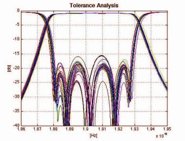
A. Tolerance Analysis
For the tolerance analysis, two different sets of tolerances are considered. The first set of simulations observes the tolerances for the air cavities. Here the iris widths, the resonator lengths and the heights are investigated. The window of the analysis is set to ±10 μm, reflecting the available accuracy of the prototype fabrication process for the surface mounted part. A sequence of random numbers within the above range is applied to determine the parameter deviations.
The second set investigates the alignment of the surface mounted waveguide part and the SIW. The position of the iris is shifted in the x and z direction (Fig. 1) within a window of ±25 μm; the deviation is again determined by a respective sequence of random numbers.
Fig. 2 presents a number of simulations taken from both sets mentioned above. Only the runs with the largest deviations compared to the optimized design are displayed. This result proves the validity and the robustness of the proposed design. The worst-case deviation for the S11 parameter is within +4 dB, still well below an absolute S11 value of -15 dB. As another result of this analysis, the manufacturing accuracy of the air cavities/resonators appears to be more critical than the actual placement of the resonators in reference to the irises in the top metallization of the SIW. Within the observed parameters of the first set, the iris widths and resonator lengths have been proven to be more critical towards the overall performance of the simulated filter when compared to the influence of the resonator’s height. Of course, such behavior is expected from standard inductively coupled waveguide filters but is not necessarily obvious in E-plane coupled structures such as shown in Fig. 1.
B. Single Resonator Loss Analysis
A simulation using CST Microwave Studio’s eigenmode solver is carried out to exactly identify the resonances of the structure. In this way, it is possible to obtain the unloaded Q factor showing the occurring losses. The related Q factors are presented in Table I for each resonating coupled cavity (Fig. 1). They are divided into volume and conductor losses noted as electrical and dielectric losses in (1).
1 |
|
1 |
|
1 |
|
1 |
(1) |
|
Q |
Q |
Q |
Q |
|||||
|
|
|
|
|||||
total |
|
electric |
|
dielectric |
|
radiation |
|
Occurring radiation through the SIW walls is also contained in the dielectric losses in Table I. It can be observed that there
are only little volume (dielectric) losses, in the range of 9 to 20 percent, for the three middle resonators (2-4), as expected, whereas resonators 1 and 5, which are coupled through the irises in the substrates’ metallization, show higher volume losses. These high volume losses can be attributed to the dielectric losses occurring in the SIW part feeding the signal to resonators one and five. Moreover, the unloaded Q factor for those two cavities is with approximately 600 slightly above the expected range of dielectric filled resonators. Unloaded Q factors of such structures are typically reported in the literature with 300-500, e.g. [8] or [14, 15].
Fig. 2. Analysis of S parameters for manufacturing tolerances of air cavities and alignment of surface mounted device versus printed circuit board.
TABLE I SINGLE RESONATOR QUALITY FACTORS (CST)
Res. # |
1 |
2 |
3 |
4 |
5 |
avg. |
|
|
|
|
|
|
|
Q con. |
51% |
87% |
91% |
82% |
51% |
72% |
|
|
|
|
|
|
|
Q vol. |
49% |
13% |
9% |
18% |
49% |
28% |
|
|
|
|
|
|
|
Q total |
612 |
2101 |
2210 |
2046 |
598 |
1513 |
|
|
|
|
|
|
|
C. Final Implementation and Fabrication of Prototype
The SMW filter will be part of an overall PCB sub-circuit design. These consider commonly large-scale production of compact designs at low cost. Thus for the final implementation, the SMW filter will consist of a housing part containing cavities and irises. This will be made with thin walls by a precise milling, casting or deep-drawing process. The housing will be combined with the substrate by a solder joint (or conductive glue bond). Thus the substrate will be prepared with a solder mask at the cavity walls and irises. (This is similar to all other components generally considered in PCB sub-circuit design). The implementation of the SMW filter can be performed according to established processes for PCBs – they will be precisely placed together with all other components (e.g. automatically by pick-and place) on the PCB prior to passing a reflow solder process. Consequently, the
758

filter will not occupy more space of the PCB as required for the footprint of irises and thin-wall cavities. Moreover, the substrate side opposite to that used for the filter implementation may be considered for connections or implementation of other components that have no bearing on the filter design but allow the overall optimization of the PCB sub-circuit application. This may be an additional advantage over a SIW implementation where the utilization of this area is not possible.
Prior to such an optimized production implementation of the SMW technology, a simpler prototype realization has been employed for the general validation of the SMW filter approach.
The four manufactured parts before assembly are displayed in Fig. 3. The first fabrication step for the printed circuit board is the drilling of the SIW via holes. The second is the metallization of these vias using a galvanic process, adding approximately 17μm of copper to the top and bottom metallization layers of original thickness of t = 17.5 Pm, thus doubling the thickness of these coating layers to about 35 Pm. Then the coupling irises for resonator one and five are placed in the substrate’s top metallization layer. As a last fabrication step, four housing holes for the stainless steel pins, aligning the substrate and the air cavities, as well as the tensioning screw housings are drilled. The air cavities are fabricated using “wire electrical discharge machining” (WEDM). Therefore, the top mounted cavities are split up in two parts: a contour of the coupled resonators and a lid, which is produced two times. The second part is used as a counter plate on the bottom side of the SIW for structural support.
Fig. 3. Manufactured SMW filter prototype parts before assembly and size comparison with a Canadian quarter coin.
In order to accommodate the fabrication process, an edge radius of 1.5 mm in the x-z plane is introduced to the air
cavities. All three sections, cavities and the two lids are milled out of copper blocks.
Only two out of the four possible stainless steel pins are used to avoid an over-determination when assembling the parts. Furthermore, the top surface of the SMW top copper coating and the bottom of the lid are polished to obtain an even surface and lower the surface current resistance. The conductivity between the different parts is ensured and enhanced using a very thin layer of silver paste.
III. MEASUREMENT
For the measurements, the VNA is calibrated to an x-y plane situated at the narrow ends of the SIW transformers, deembedding the microstrip-to-SIW taper, which is added for access with a test fixture. Fig. 4 (top) shows the measured results in comparison with simulations for a narrow band. Fig. 4 (bottom) displays a wider frequency range over the K-Band range. The measured S11 parameter is approximately 3-5 dB higher than the simulated one. This result is within the deviations obtained from the tolerance analysis. The difference in the two displayed measurement sets in Fig. 4 (top) is caused by air gaps between the sandwiched layers.
Fig. 4. Comparison between measured and simulated for K-Band results of the SMW filter in Fig. 3; narrowband (top), wideband (bottom).
759
Hence a lack in conductivity leads to less steepness of the filter skirts and therefore to a widening of the bandwidth. Also sensitivity in the S11 passband level to the applied tension on the fitting screws was observed.
As far as the reflection zeros are concerned, a good match for the high frequencies in the passband is observed. The agreement gradually decreases towards the lower frequencies. Also the slope at the lower passband cutoff frequency of the measurement data is flatter. Investigating the S21 parameter, one can observe a level of -2 to -1 dB in the passband. This insertion loss is higher than the simulations estimate but still well within the expected range accounting for the sandwich construction and conductivity, hence losses, between the different parts. Accordingly, the expected Q value is estimated lower than suggested in Table I but still well above a pure SIW technology filter (see measurements in [8]).
A possible attempt to overcome these losses would be to change the fabrication method as mentioned in Section IIC. By milling the cavities into a block, the need for a lid and therefore one interconnection in the stack presented in Fig.3 can be eliminated. This is expected to result in an improved conductivity of the surface mounted device, translating into fewer losses for the S21 parameter in the passband.
IV. CONCLUSION
A surface mounted waveguide filter prototype for combination of SIW and waveguide technology based on the advantages of both technologies is presented. The proposed structure inherits a fully shielded environment and high quality factors from the two used technologies at the cost of an increase in manufacturing effort (which is fully integratable in a PCB fabrication process) and a slight increase in space consumption, although in a different plane, when compared to pure SIW technology. The filter designed for K-band operation shows a coherent performance and low insertion loss for both simulations and measurements. Measured insertion loss performance in the 1-2 dB range is observed which is superior to pure SIW technology filters in the same frequency range. These results have been obtained for cavity heights of 1.5 mm, thus further improvement can be achieved when increased cavity heights are possible in a final implementation. Additionally, a tolerance analysis is presented to validate the design’s suitability and robustness for high volume fabrication. The main source of remaining losses is identified to occur in the substrate-to-air cavity coupling area. Ensuring a good conductivity in between the sandwich construction has been shown to be critical for the steepness of the filter skirts, hence the bandwidth.
ACKNOWLEDGMENT
The authors wish to acknowledge funding support for this work by the TELUS Research Grant in Wireless Communications.
REFERENCES
[1]K. Wu, “Towards system-on-substrate approach for future millimeter-wave and photonic wireless applications,” Proc. Asia-Pacific Microwave Conf., pp. 1895-1900, Yokohama, Japan, Dec. 2006.
[2]J. Hirokawa and M. Ando, “Single-layer feed waveguide consisting of posts for plane TEM wave excitation in parallel plates,” IEEE Trans. Antennas Propagat., vol. 46, pp. 625-630, May 1998.
[3]J. Bornemann and F. Taringou, “Substrate-integrated waveguide filter design using mode-matching techniques”, Proc. 41st European Microwave Conf., pp. 1-4, Manchester, UK, Oct. 2011.
[4]V.A. Labay and J. Bornemann, “E-plane directional couplers in substrate-integrated waveguide technology,” Proc. Asia-Pacific Microwave Conf., pp. 1-4, Hong Kong, Dec. 2008.
[5]Z. Kordiboroujeni, J. Bornemann and T. Sieverding, “K-Band substrate integrated waveguide T-junction diplexer design by mode-matching techniques”, Proc. Asia-Pacific Microwave Conf., pp. 1297-1299, Sendai, Japan, Nov. 2014.
[6]Z. Kordiboroujeni and J. Bornemann, “Efficient design of substrate integrated waveguide power dividers for antenna feed systems,” Proc. 7th European Conf. Antennas Propagat., pp. 344-348, Gothenburg, Sweden, Apr. 2013.
[7]D.-S. Eom, J.-D. Byun, and H.-Y. Lee, “Multilayer substrate integrated waveguide four-way out-of-phase power divider,”
IEEE Trans. Microw. Theory Techn., vol. 57, pp. 3469-3476, Dec. 2009.
[8]J. Schorer, J. Bornemann, and U. Rosenberg, “Comparison of surface mounted high quality filters for combination of substrate integrated and waveguide technology,” Proc. Asia-Pacific Microwave Conf., pp. 929-931, Sendai, Japan, Nov. 2014.
[9]T.J. Müller, W. Grabherr, and B. Adelseck, “Surface-mountable
metalized plastic waveguide filter suitable for high volume production,” Proc. 33rd European Microwave Conf., pp. 12551258, Munich, Germany, Oct. 2003.
[10]W. Menzel and M. Wetzel, “Waveguide filter integrated into a planar circuit,” Proc. 32nd European Microwave Conf., pp. 957960, Milan, Italy, Sep. 2002.
[11]X. Huang and K.-L. Wu, “A broadband u-slot coupled microstrip-to-waveguide transition,” IEEE Trans. Microw. Theory Techn., vol. 60, pp.1210-1217, May 2012.
[12]J. Schorer and J. Bornemann, “Mode matching analysis for
double-layered substrate integrated and rectangular waveguide filter technology,” Proc. Int. Conf. Computational Electromagnetics, pp. 158-160, Hong Kong, Feb. 2015.
[13]Z. Kordiboroujeni and J. Bornemann, “Designing the width of substrate integrated waveguide structures,” IEEE Microw. Wireless Compon. Lett., vol. 23, pp. 518-520, Oct. 2013.
[14]A.A. Khan, M.K. Mandal, and S. Sanyal, “Unloaded quality factor of a substrate integrated waveguide resonator and its variation with the substrate parameters,” Proc. Int. Conf. Microwave Photonics, p.1-4, Dhanbad, India, Dec. 2013.
[15]Y. Cassivi, L. Perregrini, K. Wu, and G. Conciauro, “Low-cost
and high-Q millimeter-wave resonator using substrate integrated waveguide technique,” Proc. 32nd European Microwave Conf., pp. 737-740, Milan, Italy, Sep. 2002.
760