

диафрагмированные волноводные фильтры / e4c17243-8b45-4393-90ee-60057daeabf3
.pdfIEEE TRANSACTIONS ON ANTENNAS AND PROPAGATION, VOL. 63, NO. 7, JULY 2015 |
3291 |
monopolar-RWG discretization of the EFIE with wedge testing performs in a similar manner as described in [6] for tetrahedral testing elements. These implementations reach, for the sharp-edged conductors tested, much wider ranges of heights of the testing elements with improved accuracy (at least two orders of magnitude bigger than for the volumetric monopolar-RWG discretization and wedge testing).
For composite objects meshed with nonconformal triangulations where neighboring triangles have no matching edges, the volumetric monopolar-RWG discretization of the EFIE with testing over right triangular prisms appears as a more reliable option than the choice with tetrahedral testing because the computed RCS becomes more stable in terms of the heights of the testing elements. The even-surface oddvolumetric monopolar-RWG implementation, though, which assigns unknowns to the edges between pairs of adjacent facets, is not amenable in general to such triangulations.
We believe that the better suitability of the wedges as testing elements when compared with the tetrahedral elements lies in the fact that the wedge-monopolar testing functions enforce the null condition for the component of the inner electric field tangential to the boundary surface, which shows better consistency with the electric-field boundary condition at the surface.
REFERENCES
[1]S. M. Rao, D. R. Wilton, and A. W. Glisson, “Electromagnetic scattering by surfaces of arbitrary shape,” IEEE Trans. Antennas Propag., vol. 30, no. 3, pp. 409–418, May 1982.
[2]R. D. Graglia, D. R. Wilton, and A. F. Peterson, “Higher order interpolatory vector bases for computational electromagnetics,” IEEE Trans. Antennas Propag., vol. 45, no. 3, pp. 329–342, Mar. 1997.
[3]M. Carr, E. Topsakal, and J. L. Volakis, “A procedure for modeling material junctions in 3-D surface integral equation approaches,” IEEE Trans. Antennas Propag., vol. 52, no. 5, pp. 1374–1379, May 2004.
[4]P. Ylä-Oijala, M. Taskinen, and J. Sarvas, “Surface integral equation method for general composite metallic and dielectric structures with junctions,” Prog. Electromagn. Res., vol. 52, pp. 81–108, 2005.
[5]E. Ubeda, J. M. Rius, and A. Heldring, “Discretization of the EFIE in method of moments without continuity of the normal current component across edges,” in Proc. IEEE Antennas Propag. Soc. Int. Symp., Orlando, FL, USA, Jul. 7–13, 2013, pp. 448–449.
[6]E. Ubeda, J. M. Rius, and A. Heldring, “Nonconforming discretization of the electric-field integral equation for closed perfectly conducting objects,” IEEE Trans. Antennas Propag., vol. 62, no. 8, pp. 4171–4186, Aug. 2014.
[7]E. Ubeda and J. M. Rius, “Monopolar divergence-conforming and curlconforming low-order basis functions for the electromagnetic scattering analysis,” Microw. Opt. Technol. Lett., vol. 46, no. 3, pp. 237–241, Aug. 2005.
[8]D. R. Wilton et al., “Potential integrals for uniform and linear source distributions on polygonal and polyhedral domains,” IEEE Trans. Antennas Propag., vol. 32, no. 3, pp. 276–281, Mar. 1984.
[9]D. A. Dunavant, “High degree efficient symmetrical Gaussian quadrature rules for the triangle,” Int. J. Numer. Methods Eng., vol. 21, pp. 1129– 1148, 1985.
[10]M. Gellert and R. Harbord, “Moderate degree cubature formulas for 3-D tetrahedral finite element approximations,” Commun. Appl. Numer. Methods, vol. 7, pp. 487–495, 1991.
Active Impedance of Infinite Parallel-Fed Continuous
Transverse Stub Arrays
Francesco Foglia Manzillo, Mauro Ettorre, Massimiliano Casaletti,
Nicolas Capet, and Ronan Sauleau
Abstract—This paper introduces a rigorous and effective modeling framework for the continuous transverse stub (CTS) array, based on a spectral Green’s function approach. A multimodal expansion of the equivalent currents over the slots is used to derive an accurate expression for the active impedance of an infinite array. This formula is validated through comparisons with full-wave simulations when the array scans are in principal planes. The mathematical formulation highlights the broadband properties of CTS arrays and accurately predicts the impact of the geometrical parameters on the active impedance, as a function of frequency and scan angle. The discussion of the results provides physical insights to outline effective design strategies.
Index Terms—Antenna arrays, broadband antennas, Green’s function, long slots, parallel plate waveguides (PPWs).
I. INTRODUCTION
The advances in Ka-band and millimeter-wave (mm-wave) technologies have led to the development of high-performance systems for satellite and wireless communication. The high losses that characterize these applications demand for wideband and high gain antennas. Reflector and dielectric lens antennas [1] achieve high gain but require nonplanar structures, not suited for installation on moving carriers. Planar arrays of printed antennas, e.g., microstrip patches, can be integrated in low profile front-ends but are limited in bandwidth and efficiency. Waveguide slot arrays represent highly efficient options, whether implemented in standard metallic [2] or substrate integrated waveguides [3]; however, their impedance bandwidths rarely exceed 20%.
An inherently broadband and high-gain antenna solution is the continuous transverse stub (CTS) array [4]–[6]. We focus on the parallel-fed CTS array that exhibits wider band performance, compared to the serial-fed configuration [6]. It comprises an array of slots in a metallic plane, fed by a corporate network in parallel plate waveguide (PPW) technology. As for connected arrays [7]–[10], the mutual coupling among the slots is the physical mechanism underlying the ultra-wideband behavior of CTS arrays. However, CTS antennas do not require ground planes to improve the front-to-back ratio, thus enhancing the bandwidth [7], [8] and reducing the antenna size. Moreover, CTS arrays can be parallel-fed by just N feeds, as
Manuscript received August 25, 2014; revised February 06, 2015; accepted April 18, 2015. Date of publication April 29, 2015; date of current version July 02, 2015. This work was supported in part by the European Union Seventh Framework Programme (FP7/2007-2013) under Grant agreement 619563 (MiWaveS) and in part by the CNES.
F. Foglia Manzillo, M. Ettorre, and R. Sauleau are with the Institute of Electronics and Telecommunications of Rennes (IETR), UMR CNRS 6164, University of Rennes 1, 35042 Rennes, France (e-mail: francesco.foglia- manzillo@univ-rennes1.fr).
M.Casaletti is with the Sorbonne Universités, UPMC University of Paris 06, F-75005, Paris, France (e-mail: massimiliano.casaletti@upmc.fr).
N.Capet is with CNES, Antenna Department, Toulouse 31401, France (e-mail: nicolas.capet@cnes.fr).
Color versions of one or more of the figures in this communication are available online at http://ieeexplore.ieee.org.
Digital Object Identifier 10.1109/TAP.2015.2427874
0018-926X © 2015 IEEE. Personal use is permitted, but republication/redistribution requires IEEE permission. See http://www.ieee.org/publications_standards/publications/rights/index.html for more information.

3292 |
IEEE TRANSACTIONS ON ANTENNAS AND PROPAGATION, VOL. 63, NO. 7, JULY 2015 |
Fig. 1. Geometry of a parallel-fed, infinite CTS array with slot width a and periodicity d. Dielectric-filled open-ended PPWs radiate into an arbitrary planelayered medium. Only one dielectric sheet of thickness h is shown for clarity. The array can be fed by a corporate feeding network illuminated by a line source.
where νm = 1 for m = 0 and νm = 2 for m = 0. The transverse component of the vector wavenumber for both TE and TM modes
'
is given by kt,T E = kt,T M = (mπ/a)2 + η2. We consider η = ky0 = k0 sin θ0 sin φ0, where k0 is the wavenumber in free space and (θ0, φ0) is the pointing direction of the array. From (1) and (2), the transverse fields Eg, Hg guided in the PPW centered at x = a/2, are derived for z = 0 as follows:
+∞ |
|
|
bT E |
|
|
bT M |
cos |
|
mπ |
x |
e |
|
|
xˆ |
|||||||
Eg = m=0 |
YmT E Vm |
|
− YmT M Vm |
|
a |
|
|
|
|
||||||||||||
|
|
|
m |
T E |
|
m |
|
T M |
|
|
|
|
|
|
|
−jky0y |
|
||||
+∞ |
|
cT M |
|
|
|
cT E |
sin |
|
mπ |
x |
e |
|
|
yˆ |
(3) |
||||||
+ m=1 YmT M Vm |
|
− YmT E Vm |
|
|
a |
|
|
||||||||||||||
|
|
|
m |
T M |
|
m |
|
T E |
|
|
|
|
|
|
|
−jky0y |
|
|
|||
+∞ |
|
|
T E |
T E |
|
T M |
|
T M |
|
mπ |
|
|
|
|
|
|
|
||||
|
|
|
|
|
|
|
|
|
|
|
|
|
|||||||||
Hg = m=1 cm |
Vm |
− cm |
Vm sin |
a |
x e−jky0y xˆ |
|
|
||||||||||||||
|
|
|
|
|
|
|
|
|
|
|
|
|
|
|
|
|
|
|
|
|
|
opposed to connected arrays demanding a tightly spaced N × N feeding system [9], [10].
Broadband CTS antennas with gain ≥30 dBi have been reported at mm-waves, both for communications in Ka-band [6] and E-band [11] and for W-band radars [12]. Nevertheless, to the best of authors’ knowledge, no analytical models of CTS antennas have been reported, nor rigorous design procedures have been clearly outlined. Numerical solutions, based on Floquet modes solutions [4], [13] or finite-difference time-domain (FDTD) method [14], have been used to design series-fed CTS arrays but not systematically described.
In this communication, we present an analytical model for infinite PPW-fed CTS arrays, based on a spectral domain integral equation approach. A multimodal expansion of the magnetic current is introduced to accurately predict the active impedance even for large scan angles. In Section II, the proposed model is derived and the assumptions it relies on are discussed. Section III presents a numerical validation via comparison with full-wave simulations. In Section IV, the impact of each parameter on the active impedance is investigated for different scan angles. Design strategies to achieve brodband, wide-angle scanning operation are given through practical examples. Conclusion is drawn in Section V.
|
+∞ |
|
|
|
T E |
|
T E |
|
T M |
|
|
|
|
T M |
mπ |
|
|
|
|
|||||||||||||||||
|
|
|
|
|
|
|
|
|
|
|
|
|
|
|
|
|
||||||||||||||||||||
+ m=0 bm |
Vm |
− bm |
Vm |
cos |
|
a |
|
x e−jky0y yˆ (4) |
||||||||||||||||||||||||||||
where |
|
|
|
|
|
|
|
|
|
|
|
|
|
|
|
|
|
|
|
|
|
|
|
|
|
|
|
|
|
|
|
|
|
|
||
|
|
|
|
|
|
|
|
|
|
|
|
|
|
|
|
|
|
|
|
|
|
|
|
|
|
|
|
|
|
|
|
|
|
|
|
|
|
|
|
|
|
|
√ |
|
|
jky0 YmT E |
|
|
|
|
|
|
|
|
|
√ |
|
|
|
|
mπ/a YmT M |
||||||||||||
T E |
|
|
|
νm |
|
|
|
|
|
T M |
|
|
|
νm |
||||||||||||||||||||||
bm |
= |
|
|
|
|
|
|
|
|
|
|
|
|
|
|
|
, |
bm = |
|
|
|
|
|
|
|
|
|
|
|
|
|
|
||||
√ |
|
|
|
|
|
|
|
|
|
|
|
|
|
√ |
|
|
|
|
|
|
|
|
|
|
|
|
||||||||||
|
|
|
'k |
2 |
|
|
mπ/a)2 |
|
2 |
+ (mπ/a)2 |
||||||||||||||||||||||||||
|
|
|
|
|
|
|
|
|
||||||||||||||||||||||||||||
|
|
|
|
|
a |
y0 + ( |
T E |
|
|
|
|
|
|
|
|
a'ky0 |
T M |
|||||||||||||||||||
|
|
|
|
|
|
|
|
|
|
|
|
|
|
|
|
|
|
|
|
|||||||||||||||||
cmT E = |
|
|
√νmmπ/a Ym |
|
|
, |
|
cmT M = |
|
|
|
√νmjky0 Ym |
|
. |
||||||||||||||||||||||
√ |
|
|
|
|
|
|
|
|
|
|
|
|
|
|
√ |
|
|
|
|
|||||||||||||||||
|
|
|
|
|
|
|
|
|
|
|
|
|
|
|
|
|
|
|||||||||||||||||||
|
|
a |
'ky20 + (mπ/a)2 |
|
|
a |
'ky20 + (mπ/a)2(5) |
|||||||||||||||||||||||||||||
The scalar modal functions for TE and TM modes VmT E,T M (z) |
|||||||||||||
are |
measured in |
V/√ |
|
|
and |
VmT E,T M = VmT E,T M (z = 0). |
|||||||
m |
|||||||||||||
The |
modal |
admittances |
for TE |
and TM modes |
[15] are |
||||||||
|
|
|
|
|
|
|
|
|
|
||||
given |
by |
|
YmT E = |
|
k2 − (mπ/a)2 − ky20/ (ζ k) and |
YmT M = |
|||||||
|
|
|
2 |
|
|
2 |
|
2 |
|
|
|
|
|
k/(ζ |
k |
|
|
' |
|
|
|
|
|
||||
|
− (mπ/a) − ky0), where k and ζ are the wavenumber |
||||||||||||
and the impedance of the medium in the PPW. |
|
||||||||||||
|
' |
|
|
|
|
|
|
|
|
|
|
|
|
The incident fields are assumed mono-modal (pure T E0 modes), equal in amplitude and progressively shifted in phase to steer the beam in (θ0, φ0). The incident magnetic field Hi on xy-plane (z = 0) has thus the following expression:
|
II. ANALYTICAL MODEL |
|
|
|
|
|
T E |
V i e−jky0y |
+∞ |
|
|
a |
|
|
|
|
||||||||||||||||||||||
The geometry of the problem is shown in Fig. 1. An infinite array of |
Hi = jY0 |
|
√a |
|
n=−∞ Πa x − |
2 − nd e−jkx0nd yˆ (6) |
||||||||||||||||||||||||||||||||
rectangular slots of width a and infinite length along y-axis is placed |
|
|
|
|
|
|
|
|
|
|
|
|
|
|
|
|
|
|
||||||||||||||||||||
where |
kx0 |
= k0 |
sin θ |
cos φ |
|
, and Π |
|
(x) = 1 for x |
|
( |
− |
a/2, a/2) |
||||||||||||||||||||||||||
along x-direction in a metal plane. The inter-element spacing is d. The |
0 |
a |
||||||||||||||||||||||||||||||||||||
|
|
|
0 i |
|
|
|
|
|
|
|
|
|
||||||||||||||||||||||||||
incident fields propagate along z-direction in ideal PPWs. All metals |
and null elsewhere. V |
is the known scalar modal function of the |
||||||||||||||||||||||||||||||||||||
are assumed perfect conductors. The model accounts for slots fed by |
incident field. |
|
|
|
|
|
|
|
|
|
|
|
|
|
|
|
|
|
||||||||||||||||||||
dielectric-filled PPWs radiating in a layered medium (only one layer is |
The discontinuity at z = 0 gives rise to another wave in the region |
|||||||||||||||||||||||||||||||||||||
shown in Fig. 1). The array can be practically fed by a PPW corporate |
z > 0, besides the incident field. It can be interpreted as the field |
|||||||||||||||||||||||||||||||||||||
feeding network, whose input line is illuminated by a linear source, |
reflected back from the slots into the PPWs and will be referred to as |
|||||||||||||||||||||||||||||||||||||
e.g., a pillbox coupler [3], [4] or a slotted waveguide array, to allow |
reflected field. This field is a solution of Maxwell’s equations in a PPW |
|||||||||||||||||||||||||||||||||||||
for beam-scanning. |
|
|
|
|
|
|
|
|
|
|
|
region. Therefore, it is analytically described by (3) and (4), except for |
||||||||||||||||||||||||||
In a PPW, the scalar potentials ψT E and φT M for transverse elec- |
a sign that accounts for the reversed direction of propagation (negative |
|||||||||||||||||||||||||||||||||||||
tric (TE) and magnetic (TM) modes, with respect to z-axis, are given |
z semi-axis). Formally, the reflected magnetic field Hr = Hr(x, y, 0) |
|||||||||||||||||||||||||||||||||||||
by [15] |
|
|
|
|
|
|
|
|
|
|
|
|
|
|
|
|
|
at the plane z = 0 is given by |
|
|
|
|
|
|
|
|
|
|
|
|||||||||
|
|
|
|
|
|
|
|
|
|
|
|
|
|
|
|
|
|
|
|
|
|
|
∞ |
|
|
|
|
|
|
|
a |
|
|
|
|
|
||
T E |
|
|
νm |
|
|
mπ |
|
|
jηy |
|
|
|
r |
|
|
|
|
|
|
|
|
|
|
|
|
|
|
|
||||||||||
ψm |
(x, y) = & a |
|
|
cos |
|
a |
x e− |
|
|
, |
|
H = − n=−∞ Hg (x − nd, y) Πa x − 2 − nd |
||||||||||||||||||||||||||
|
|
|
|
|
|
|
|
|
|
|
|
|
|
|
|
(1) |
|
|
|
|
|
|
|
|
|
|
|
|
|
|
|
|
|
|
||||
m = 0, 1, 2, . . . , −∞ < η < +∞ |
|
|
|
|
|
× e−jkx0nd . |
|
|
|
|
|
|
|
|
|
|
|
(7) |
||||||||||||||||||||
T M |
|
2 |
|
|
|
|
|
mπ |
|
jηy |
|
|
The electric field scattered in the region z < 0 is derived from the |
|||||||||||||||||||||||||
φm |
(x, y) = & |
|
|
sin |
|
x e− |
|
|
, |
|
|
|
|
|
|
|
||||||||||||||||||||||
a |
a |
|
|
|
equivalent magnetic current Mn over the aperture plane xy. This cur- |
|||||||||||||||||||||||||||||||||
m = 1, 2, 3, . . . , −∞ < η < +∞ |
|
|
(2) |
rent is related by the equivalence theorem to the unknown aperture |
||||||||||||||||||||||||||||||||||

IEEE TRANSACTIONS ON ANTENNAS AND PROPAGATION, VOL. 63, NO. 7, JULY 2015 |
3293 |
field Ea. A straightforward expansion of Ea in infinite PPW modes, as in (3), leads to an effective expression for Mn
Mn(x, y) = −zˆ × Ea|z=0 |
(8) |
||
∞ |
a |
− nd e−jkx0nd. |
(9) |
Ea = n=−∞ Eg(x − nd, y) Πa x − |
2 |
||
|
|
|
|
The tangential component of the transmitted magnetic field at z = 0, denoted as Ht = Ht(x, y, 0), is given by the convolution of Mn with GtHM , the transverse dyadic Green’s function of the upper half-space
for the magnetic field, evaluated for z = 0
Ht = GtHM (x − x , y − y )Mn(x , y )dx dy . (10)
R2
The computation of (10) is straightforward if performed in the spectral (kx, ky) domain. After some algebraic steps and an inverse Fourier transform, the x and y components of the transmitted magnetic field at z = 0 are found to be
In order to find the unknown equivalent current, i.e., the coefficients VmT E , VmT M , the continuity of the tangential component of the magnetic field is enforced over the slot S0 centered at x = a/2. As the incident magnetic field has only y component, the equations to be solved are
Hxr(x, y, 0)|S0 |
= Hxt (x, y, 0)|S0 |
(15) |
Hyi (x, y, 0)|S0 |
+ Hyr(x, y, 0)|S0 = Hyt (x, y, 0)|S0 . |
(16) |
An approximate solution can be found by considering 2M − 1 expansion modes (M TE modes and M − 1 TM modes) and 2Nf + 1 Floquet modes. Both sides of (15) and (16) are averaged with two sets of basis functions in the domain S0. The set of basis functions sin (pπx/a), p = 1, . . . , M − 1 is chosen for (15) and the set cos (qπx/a), q = 0, 1, . . . , M − 1 for (16), both in the domain x [0, a]. The two sets of equations obtained can be rearranged in a standard block matrix formed by grouping TE and TM components, yielding
|
|
Y T E,T E Y T E,T M |
VTE |
|
I0 |
|
|
||||
|
|
T M,T E |
|
|
T M,T M |
VTM |
|
0 |
|
(17) |
|
Y |
Y |
||||||||||
|
t |
|
e−jky0y +∞ |
|
|
|
|
cmT M |
|
T M |
|
|
|
cmT E |
|
|
|
T E |
|
|
|
where |
|
|
|
|
|
|
|
|
|
|
|
|
T E |
|
|
|
|
T E |
|
|
|
|
T E |
|
|
|
|
and |
|
|
VT M = |
||||||||||||||||||||||||||||||||
|
Hx = |
|
|
|
|
|
|
|
|
|
|
|
|
|
|
|
|
|
|
|
|
|
Vm |
|
|
|
|
|
Vm |
|
|
|
|
|
|
VT E = V0 |
|
|
|
, V1 |
|
|
|
, . . . , VM−1 |
|
|
|
|
|
||||||||||||||||||||||||||||||||||||
|
|
|
|
|
|
|
|
|
|
|
|
|
|
|
|
|
|
|
|
T M |
|
|
|
T E |
|
|
|
|
|
|
|
|
|
|
|
|
|
|
|||||||||||||||||||||||||||||||||||||||||||||||
|
|
|
|
d |
|
|
|
|
m=1 Ym |
|
|
|
− Ym |
|
|
|
|
|
|
|
|
|
|
T M |
T M |
|
|
|
|
|
|
|
T M |
|
|
|
|
|
are |
|
|
the |
unknown |
coefficients |
of |
the |
|||||||||||||||||||||||||||||||||||||||
|
|
|
|
|
|
|
|
|
|
|
|
|
|
|
|
|
|
|
|
V1 |
, V2 |
|
, . . . , VM |
|
|
1 |
|
|
|
|
|
|
|||||||||||||||||||||||||||||||||||||||||||||||||||||
|
|
|
|
+ |
|
|
|
|
|
|
|
|
|
|
|
|
|
|
|
|
|
|
|
|
|
|
|
|
|
|
|
|
|
|
|
|
|
|
|
|
|
|
|
|
|
|
|
|
|
− |
|
|
|
|
|
|
|
i |
|
|
|
|
|
T E |
|
|
|
|
|
|
|
|
|
|
|
|
|||||||||
|
|
|
|
|
|
|
|
|
|
|
|
|
|
|
|
|
|
|
|
|
|
|
|
|
|
|
|
|
|
|
|
|
|
|
|
|
|
|
|
|
|
|
|
|
|
|
|
|
|
|
|
|
|
|
|
|
|
|
|
|
|
|
|
|
|
|
|
|
|||||||||||||||||
|
|
|
|
∞ |
|
|
|
|
|
|
|
|
|
|
|
|
|
|
|
|
|
|
|
|
|
|
|
|
|
|
|
|
|
|
|
|
|
|
|
current expansion; |
I0 |
= jV |
|
√aY0 |
|
, 0, . . . , 0 |
|
is the M-elements |
|||||||||||||||||||||||||||||||||||||
|
|
× |
|
|
|
|
|
|
|
|
|
|
|
|
|
|
|
|
|
HM |
(kxn, ky0)e− |
jk |
|
|
x |
|
|
|
|
|
|
|
|
|
|
|
|
|
|
|
|||||||||||||||||||||||||||||||||||||||||||||
|
|
|
|
|
|
|
|
Γm(kxn)G˜xx |
|
|
xn |
|
|
|
|
vector of the excitations, all null except for the fundamental mode. |
|||||||||||||||||||||||||||||||||||||||||||||||||||||||||||||||||||||
|
|
|
n=−∞ |
|
|
|
|
|
|
|
|
|
|
|
|
|
|
|
|
|
|
|
|
|
|
|
|
|
|
|
|
|
|
|
|
|
Every |
field can be |
|
calculated |
after |
solving (17) for VTE, VTM. |
|||||||||||||||||||||||||||||||||||||||||||
|
|
|
|
|
|
|
|
|
|
|
|
|
|
|
|
|
|
|
|
|
|
|
|
|
|
|
|
|
|
|
|
|
|
|
|
|
|
|
|
Explicit expressions for the elements of matrices Y T ·,T · in (17) are |
|||||||||||||||||||||||||||||||||||||||||||||
|
|
|
|
e−jky0y +∞ |
|
|
|
|
bmT M |
|
T M |
|
bmT E |
|
|
|
T E |
|
|||||||||||||||||||||||||||||||||||||||||||||||||||||||||||||||||||
|
|
+ |
|
|
|
|
|
|
|
|
|
|
|
|
|
|
|
|
Vm |
|
|
|
− |
|
|
Vm |
|
|
given below: |
|
|
|
|
|
|
|
|
|
|
|
|
|
|
|
|
|
|
|
|
|
|
|
|
|
|
|
|
|
|
|
|
|
|
|
|
|
|
|
|||||||||||||||||
|
|
|
|
|
|
|
|
|
|
|
|
|
|
|
|
|
|
|
|
|
|
|
|
|
|
|
|
|
|
|
|
|
|
|
|
|
|
|
|
|
|
|
|
|
|
|
|
|
|
|
|
|
|
|
|
|
|
|
|
|
|
|
|
|
|
|
|
|
|||||||||||||||||
|
|
|
|
|
d |
|
|
|
|
|
|
m=0 |
YmT M |
|
|
|
YmT E |
|
|
|
|
|
|
|
|
|
|
|
|
|
|
|
|
|
|
|
|
|
|
|
|
|
|
|
|
|
|
|
|
|
|
|
|
|
|
|
|
||||||||||||||||||||||||||||
|
|
|
|
+∞ |
|
|
|
|
|
|
|
|
|
|
|
|
|
|
|
|
|
|
|
|
|
|
|
|
|
|
|
|
|
|
|
|
|
|
|
|
|
bjT E |
|
|
|
|
|
Nf |
|
|
|
|
|
|
|
|
|
|
|
|
|
˜HM |
|
|
|
|
|
|
|||||||||||||||||
|
|
|
|
|
|
|
|
|
|
|
|
|
|
|
|
|
|
|
|
|
|
|
|
|
|
|
|
|
|
|
|
|
|
|
|
|
|
|
|
T E,T E |
|
|
|
|
|
|
|
|
|
|
|
|
|
|
|
|
|
|
|
|
|
|
|
|
− |
|
|
|
|
|
|
|
|
|
|||||||||||
|
|
× |
|
|
|
|
|
|
|
|
|
|
|
|
|
|
|
|
|
|
|
˜HM |
(kxn, ky0)e |
−jkxnx |
|
|
(11) |
|
Yij |
|
= |
|
|
|
|
|
|
|
|
|
|
|
|
|
|
|
|
|
Λj (kxn)Λi( |
kxn)Gyy |
|
|
|
|
|
|
|||||||||||||||||||||||||||||
|
|
|
|
|
|
|
|
|
|
|
|
|
|
|
|
|
|
|
|
|
|
|
|
|
|
|
|
|
T E |
d |
|
|
|
|
|
|
|
|
|
|
|
|
|
|
|
||||||||||||||||||||||||||||||||||||||||
|
|
|
|
|
|
|
|
Λm(kxn)Gxy |
|
|
|
|
|
|
|
|
|
|
|
|
|
− Yj |
|
|
|
n=−Nf |
|
|
|
|
|
|
|
|
|
|
|
|
|
|
|
|
|
|
|||||||||||||||||||||||||||||||||||||||||
|
|
|
n= |
|
|
|
|
|
|
|
|
|
|
|
|
|
|
|
|
|
|
|
|
|
|
|
|
|
|
|
|
|
|
|
|
|
|
|
|
|
|
|
|
|
|
|
|
|
|
|
|
|
|
|
|
|
|
|
|
|
|
|
|
|
|
|
|
|
|
|
|
|
|
||||||||||||
|
|
|
|
|
|
−∞ |
|
|
|
|
|
|
|
|
|
|
|
|
|
|
|
|
|
|
|
|
|
|
|
|
|
|
|
|
|
|
|
|
|
|
|
|
|
|
|
|
|
|
|
|
|
|
|
|
|
|
|
|
|
|
|
|
|
|
|
|
|
|
|
|
|
|
|
|
|
|
|
||||||||
|
|
|
|
|
|
|
|
|
|
|
|
|
|
|
|
|
|
|
|
|
|
|
|
|
|
|
|
|
|
|
|
|
|
|
|
|
|
|
|
|
|
|
|
|
|
|
|
|
|
|
|
|
|
Nf |
|
|
|
|
|
|
|
|
|
|
|
|
|
|
|
|
|
|
|
|
|
|
|
|
|
||||||
|
t |
|
e−jky0y +∞ |
|
|
|
|
cmT M |
|
T M |
|
|
|
cmT E |
|
|
|
T E |
|
|
|
|
|
|
|
|
|
cjT E |
|
|
|
|
|
|
|
|
|
|
|
|
|
|
|
|
|
|
|
|
˜HM |
a |
T E |
|
|||||||||||||||||||||||||||||||||
|
Hy = |
|
|
|
|
|
|
|
|
|
|
|
|
|
Vm |
− |
|
Vm |
|
|
|
|
|
|
|
− |
|
|
|
n= |
|
|
Nf Γj (kxn)Λi(−kxn)Gyx + |
|
|
bj |
|
δij , |
|||||||||||||||||||||||||||||||||||||||||||||||
|
|
|
d |
|
|
|
|
m=1 |
YmT M |
YmT E |
|
|
|
|
|
|
YjT E d |
− |
νj |
|
|||||||||||||||||||||||||||||||||||||||||||||||||||||||||||||||||
|
|
|
|
+∞ |
|
|
|
|
|
|
|
|
|
|
|
|
|
|
|
|
|
|
|
|
|
|
|
|
|
|
|
|
|
|
|
|
|
|
|
|
|
|
|
|
|
|
|
|
|
|
|
|
|
|
|
|
|
|
|
|
|
|
|
|
|
|
|
|
|
|
|
|
(18) |
||||||||||||
|
|
|
|
|
|
Γm(kxn)G˜HM |
(kxn, ky0)e−jkxnx |
|
|
|
|
|
|
for i = 0, 1, . . . M − 1, j = 0, 1, . . . M − 1 |
|
|
|||||||||||||||||||||||||||||||||||||||||||||||||||||||||||||||||||||
|
|
× n=−∞ |
|
|
|
|
|
|
|
|
|||||||||||||||||||||||||||||||||||||||||||||||||||||||||||||||||||||||||||
|
|
|
|
|
|
|
|
|
|
|
|
|
|
|
yx |
|
|
|
|
|
|
|
|
|
|
|
|
|
|
|
|
|
|
|
|
|
|
|
|
bT M |
|
|
|
|
Nf |
|
|
|
|
|
|
|
|
|
|
|
|
˜HM |
|
|
|
|
|
|
|||||||||||||||||||||
|
|
|
|
|
|
|
|
|
|
|
|
|
|
|
|
|
|
|
|
|
|
|
|
|
|
|
|
|
|
|
|
|
|
|
|
|
|
|
|
|
T E,T M |
|
|
|
|
|
j |
|
|
|
|
|
|
|
|
|
|
|
|
|
|
|
|
|
|
|
|
|
|
|
|
|
|
|
|
|
|
||||||||
|
|
|
|
|
−jky0y +∞ |
|
|
|
|
|
|
|
|
|
|
|
|
|
|
|
|
|
|
|
|
Yij |
|
= |
|
|
|
|
|
|
|
|
|
|
|
|
|
|
Λj (kxn)Λi(−kxn)Gyy |
|
|
|
|
|
|
||||||||||||||||||||||||||||||||||||
|
|
|
|
e |
|
|
|
|
T M |
|
|
|
|
|
|
T E |
|
|
|
|
|
|
|
|
|
|
|
Y T M d |
|
|
|
|
|
|
|
|
|
|
|
|
|
|
|
|
|||||||||||||||||||||||||||||||||||||||||
|
|
+ |
|
|
|
|
|
|
|
|
|
|
|
|
|
|
|
|
|
|
bm |
|
VmT M |
|
bm |
|
|
VmT E |
|
|
|
|
|
|
|
|
j |
|
|
|
n=−Nf |
|
|
|
|
|
|
|
|
|
|
|
|
|
|
|
|
|
|
|
|
|
|||||||||||||||||||||||
|
|
|
|
|
|
|
|
|
|
|
|
m=0 YmT M |
− YmT E |
|
|
|
|
|
|
|
|
|
|
|
|
|
|
|
|
|
|
|
|
|
|
|
|
|
|
|
|
|
|
|
|
|
|
|
|||||||||||||||||||||||||||||||||||||
|
|
|
|
|
|
|
d |
|
|
|
|
|
|
|
|
|
|
|
|
|
|
|
|
|
|
|
|
|
|
|
|
|
|
|
|
|
|
|
|
|
|
|
|
|
|
|
|
Nf |
|
|
|
|
|
|
|
|
|
|
|
|
|||||||||||||||||||||||||
|
|
|
|
|
|
|
|
|
|
|
|
|
|
|
|
|
|
|
|
|
|
|
|
|
|
|
|
|
|
|
|
|
|
|
|
|
|
|
|
|
a T M |
|
|
|
|
|
|
|
|
|
cT M |
|
|
|
|
|
|
|
|
|
|
|
|
|
|
|
|
|
|||||||||||||||||
|
|
|
|
|
|
|
|
|
|
|
|
|
|
|
|
|
|
|
|
|
|
|
|
|
|
|
|
|
|
|
|
|
|
|
|
|
|
|
|
|
|
|
|
|
|
|
|
|
|
|
|
|
|
|
|
|
|
j |
|
|
|
|
|
|
|
|
|
|
|
|
|
|
|
|
|
|
HM |
||||||||
|
|
|
|
+∞ |
|
|
|
|
|
|
|
|
|
|
|
|
|
|
|
|
|
|
|
|
|
|
|
|
|
|
|
|
|
|
|
|
− |
|
|
bj |
|
|
δij + |
|
|
|
|
|
|
Γj (kxn)Λi(−kxn)G˜yx , |
|||||||||||||||||||||||||||||||||||
|
|
× |
|
|
|
|
|
|
|
|
|
|
|
|
|
|
|
˜HM |
(kxn, ky0)e− |
jkxnx |
|
|
(12) |
|
|
|
|
2 |
|
|
|
Y T M d |
|
||||||||||||||||||||||||||||||||||||||||||||||||||||
|
|
|
|
|
|
|
|
Λm(kxn)Gyy |
|
|
|
|
|
|
|
|
|
|
|
|
|
|
|
|
|
|
|
|
|
|
|
|
|
|
|
|
j |
|
|
|
|
|
n=−Nf |
|
|
|
|
|
|
|
|
|
|
|
|
||||||||||||||||||||||||||||||
|
|
|
|
|
|
|
|
|
|
|
|
|
|
|
|
|
|
|
|
|
|
|
|
|
|
|
|
|
|
|
|
|
|
|
|
|
|
|
|
|
|
|
|
|
|
|
|
|
|
|
|
|
|
|
|
|
|
|
|
|
|
|
|
|
|
|
|
|
|
|
|
|
|
|
|
|
|
|
|
||||||
|
|
|
n=−∞ |
|
|
|
|
|
|
|
|
|
|
|
|
|
|
|
|
|
|
|
|
|
|
|
|
|
|
|
|
|
|
|
|
|
|
|
|
|
|
|
|
|
|
|
|
|
|
|
|
|
|
|
|
|
|
|
|
|
|
|
|
|
|
|
|
|
|
|
|
|
|
|
|
|
|
|
|
||||||
|
|
|
|
|
|
|
|
|
|
|
|
|
|
|
|
|
|
|
|
|
|
|
|
|
|
|
|
|
|
|
|
|
|
|
|
|
|
|
|
|
|
|
for i = 0, 1, . . . M − 1, j = 1, 2 . . . M − 1 |
|
|
|
|
|
(19) |
||||||||||||||||||||||||||||||||||||
|
|
|
|
|
|
|
|
|
|
|
|
|
|
|
|
|
˜HM |
|
|
|
|
|
|
|
|
|
|
|
|
|
|
|
|
|
|
|
|
|
|
|
|
|
|
||||||||||||||||||||||||||||||||||||||||||
where |
|
|
|
|
|
|
|
|
|
|
|
|
|
|
|
|
is the Fourier transform of the |
|
|
|
|
|
|
|
|
T E |
|
|
|
|
|
Nf |
|
|
|
|
|
|
|
|
|
|
|
|
|
|
|
|
|
|
|
|
|
||||||||||||||||||||||||||||||||
kxn = kx0 − |
2πn/d, G |
ij |
|
|
|
T M,T E |
|
|
|
|
|
cj |
|
|
|
|
|
|
|
|
|
|
|
|
|
|
|
|
|
|
|
|
|
|
|
|
|
˜HM |
|
|
|
|
|
|
|||||||||||||||||||||||||||||||||||||||||
|
|
|
|
HM |
|
|
|
|
|
|
|
|
|
|
|
|
|
|
|
|
|
|
|
|
|
|
|
|
|
|
|
|
|
|
|
|
|
|
|
|
|
|
|
|
|
|
|
|
|
|
|
|
|
|
|
|
|
|
|
|
|
|
|
|
|
|
|||||||||||||||||||
(i, j)th element |
of Gt |
|
|
|
|
|
|
and can be easily derived even in the |
|
Yij |
|
= |
− YjT E d |
|
|
|
|
|
|
|
|
|
Γj (kxn)Γi(−kxn)Gxx |
|
|
|
|
|
|
||||||||||||||||||||||||||||||||||||||||||||||||||||||||
presence of layered media above the apertures, using the equivalent |
|
|
|
|
|
|
|
|
|
|
|
|
|
|
n=−Nf |
|
|
|
|
|
|
|
|
|
|
|
|
|
|
|
|
|
|
|
|||||||||||||||||||||||||||||||||||||||||||||||||||
|
|
|
|
|
|
|
|
|
|
|
|
|
|
|
|
|
|
|
|
|
|
|
|
|
|
|
|
|
|
|
|
|
|
|
|
|
|
|
|
|
|
|
|
|
|
|
|
|
|
|
|
|
|
|
|
|
|
|
|
|
|
|
|
|
|
|
|
|
|
|
|
|
|
|
|
|
|
|
|
|
|||||
transmission line technique as in [15]. The auxiliary functions Λm(kx) |
|
|
|
|
|
|
|
T E |
|
|
|
|
|
Nf |
|
|
|
|
|
|
|
|
|
|
|
|
|
|
|
|
|
|
|
a T E |
|
|
|||||||||||||||||||||||||||||||||||||||||||||||||
and Γm(kx) are defined as |
|
|
|
|
|
|
|
|
|
|
|
|
|
|
|
|
|
|
|
|
|
|
|
|
|
|
|
|
|
|
|
|
|
|
bj |
|
|
|
|
|
|
|
|
|
|
|
|
|
|
|
|
|
|
|
|
|
|
|
|
˜ |
HM |
|
|
||||||||||||||||||||||
|
|
|
|
|
|
|
|
|
|
|
|
|
|
|
|
|
|
|
|
|
|
|
|
|
|
|
|
|
|
|
− |
Y T E d |
|
|
|
|
|
|
|
|
|
|
Λj (kxn)Γi(−kxn)Gxy + |
2 |
cj |
|
δij , |
||||||||||||||||||||||||||||||||||||||
|
|
|
|
a |
|
|
|
|
|
|
|
|
|
|
|
|
|
|
|
|
|
|
|
|
|
|
|
|
|
|
|
|
|
|
|
|
|
|
|
|
|
|
|
|
|
|
|
|
|
j |
|
|
n=−Nf |
|
|
|
|
|
|
|
|
|
|
|
|
|
|
|
|
|
|
|
|
|
|||||||||||
|
|
|
|
|
|
|
|
|
|
|
mπ |
|
|
|
|
|
|
|
|
|
|
|
|
|
|
a |
|
|
|
|
|
|
|
|
|
|
|
|
|
|
|
|
|
|
|
|
|
|
|
|
|
|
|
|
|
|
|
|
|
|
|
|
|
|
|
|
|
|
|
|
|||||||||||||||
Λm(kx) = 0 |
|
|
|
|
|
|
|
|
|
|
|
|
|
|
|
|
|
|
|
|
|
a |
|
|
|
π |
|
|
|
|
|
|
|
|
|
|
|
|
|
|
|
|
|
|
|
|
|
|
|
|
|
|
|
|
|
|
|
|
|
|
|
|
|
|
|
|
|
||||||||||||||||||
|
cos |
|
|
|
|
|
|
x |
ejkxxdx = |
|
|
ejkx 2 ejm |
2 · |
|
|
|
|
|
|
for i = 1, 2 . . . M − 1, j = 0, 1, . . . M − 1 |
|
|
|
|
|
(20) |
|||||||||||||||||||||||||||||||||||||||||||||||||||||||||||
|
|
|
|
a |
|
|
2 |
|
|
|
|
|
|
|
|
|
|
|
|||||||||||||||||||||||||||||||||||||||||||||||||||||||||||||||||||
|
|
|
|
|
|
|
|
|
|
|
|
|
|
|
|
|
|
|
|
jmπ |
|
|
|
|
|
|
|
|
a |
|
|
|
mπ |
|
|
|
|
|
|
|
|
|
T M |
|
|
|
|
Nf |
|
|
|
|
|
|
|
|
|
|
|
|
|
|
|
|
|
|
|
|
|
|
|||||||||||||||
|
|
|
|
|
|
|
|
|
|
a |
|
|
mπ |
|
|
|
|
|
|
|
|
|
|
|
|
|
|
|
|
|
|
|
|
|
|
|
|
|
|
|
|
|
|
|
|
|
|
|
|
|
|
|
|
|
|
|
|
|
|
|
|
|
|
|
|
|
|
|
|
|
|
||||||||||||||
|
|
|
|
|
|
|
|
|
|
|
|
|
|
|
|
|
|
|
|
|
|
|
|
|
|
|
|
|
|
|
|
|
|
|
|
|
|
|
|
|
|
|
|
T M,T M |
|
|
|
|
bj |
|
|
|
|
|
|
|
|
|
|
|
|
|
|
|
|
|
|
|
|
|
|
|
|
|
|
HM |
|
|
|
|
|
|
|||
|
sinc kx 2 + |
|
|
|
|
|
|
+ e− |
|
|
sinc kx 2 − 2 |
|
|
|
|
|
|
|
|
|
|
|
|
|
|
|
|
|
|
|
|
|
|
|
|
|
|
|
|
|
|
|
|
|
|
||||||||||||||||||||||||||||||||||||||||
|
2 |
|
|
|
|
Yij |
|
= |
|
n= |
|
|
|
|
|
Λj (kxn)Γi(−kxn)G˜xy |
|
|
|
|
|
|
|||||||||||||||||||||||||||||||||||||||||||||||||||||||||||||||
|
|
|
|
|
|
YjT M d |
− |
N |
f |
|
|
|
|
|
|
||||||||||||||||||||||||||||||||||||||||||||||||||||||||||||||||||||||
|
|
|
|
|
|
|
|
|
|
|
|
|
|
|
|
|
|
|
|
|
|
|
|
|
|
|
|
|
|
|
|
|
|
|
|
|
|
|
|
|
|
(13) |
|
|
|
|
|
|
|
|
|
|
|
|
|
|
|
|
|
|
|
|
|
|
|
|
|
|
|
|
|
|
|
|
|
|
|
|
|
|
|
|
|||
|
|
0 |
a |
|
|
|
|
|
|
mπ |
|
|
|
|
|
|
|
|
|
|
|
|
|
|
a |
|
|
|
|
|
|
|
|
|
|
|
|
|
|
|
|
|
|
|
|
|
|
|
|
|
|
|
|
|
|
|
|
|
|
|
|
|
|
|
|
|
|
|
|
|
|
|
|
|
|||||||||||
|
|
|
|
|
|
|
|
|
|
|
|
|
|
|
|
|
|
|
|
|
|
a |
|
|
|
|
π |
|
|
|
|
|
|
|
|
|
|
|
|
|
|
|
|
|
|
|
|
|
|
|
|
|
T M |
|
|
|
Nf |
|
|
|
|
|
|
|
|
|
|
|
|
||||||||||||||||
|
|
|
|
|
|
|
|
|
|
|
|
|
|
|
|
|
|
|
|
|
|
|
|
|
|
|
|
|
|
|
|
|
|
|
|
|
|
|
|
|
|
|
|
|
|
|
|
|
|
|
|
|
|
|
|
|
|
|
|
|
|
|
|
|
|
||||||||||||||||||||
Γm(kx) = |
|
sin |
|
|
|
|
|
|
x |
ejkxxdx = |
|
|
|
ejkx |
2 ejm |
2 |
|
|
|
|
|
|
|
a |
|
T M |
|
|
|
|
|
|
cj |
|
|
|
|
|
|
|
|
|
|
|
|
|
|
|
|
|
|
HM |
|||||||||||||||||||||||||||||||||
|
|
|
|
|
|
|
|
|
|
|
|
|
|
|
|
|
|
|
|
|
|
|
|
|
|
|
|
|
|
|
|
|
|
|
|
|
|
|
|
||||||||||||||||||||||||||||||||||||||||||||||
|
|
|
|
|
|
|
|
|
a |
|
|
|
|
|
|
|
|
|
2j |
|
|
|
|
|
|
|
|
|
· |
|
|
|
|
|
− |
|
|
δij ci |
|
|
|
+ |
|
|
|
Γj (kxn)Γi(−kxn)G˜xx , |
|||||||||||||||||||||||||||||||||||||||
|
|
|
|
|
|
|
|
|
|
|
|
|
|
|
|
|
|
|
|
|
|
|
|
|
|
|
|
|
|
|
|
2 |
|
|
|
dY T M |
|
||||||||||||||||||||||||||||||||||||||||||||||||
|
|
|
|
|
|
|
|
|
|
a |
|
|
mπ |
|
|
|
|
|
|
jmπ |
|
|
|
|
|
|
|
|
a |
|
|
|
mπ |
|
|
|
|
|
|
|
|
|
|
|
|
|
|
|
|
|
|
|
|
|
|
|
|
|
|
|
|
|
n=−Nf |
|
|
|
|
|
|
|
|
|
|
|
|
||||||||||
|
sinc kx |
|
|
|
+ |
|
|
|
|
|
|
− e− |
|
|
sinc kx |
|
− |
|
(14) |
|
|
|
|
|
|
|
|
|
|
|
|
|
|
|
|
|
|
|
|
|
|
|
|
|
|
|
|
|
|
|
|
|
|
|
|
|
|
|
|
|
|
||||||||||||||||||||||||
|
2 |
2 |
|
|
|
|
2 |
2 |
|
|
|
for i = 1, 2 . . . M − 1, j = 1, 2 . . . M − 1. |
|
|
|
|
|
(21) |
|||||||||||||||||||||||||||||||||||||||||||||||||||||||||||||||||||
|
|
|
|
|
|
|
|
|
|
|
|
|
|
|
|
|
|
|
|
|
|
|
|
|
|
|
|
|
|
|
|
|
|
|
|
|
|
|
|
|
|
|
|
The Green’s functions are evaluated for kx = kxn, ky = ky0. The |
|||||||||||||||||||||||||||||||||||||||||
where m = 0, 1, . . ., and sinc (x) = sin(x)/x. |
|
|
|
|
|
|
|
|
|
|
function δij = 1 for i = j and is null elsewhere. |
|
|
|
|
|
|
|
|
|
|
||||||||||||||||||||||||||||||||||||||||||||||||||||||||||||||||

3294 |
IEEE TRANSACTIONS ON ANTENNAS AND PROPAGATION, VOL. 63, NO. 7, JULY 2015 |
III. NUMERICAL VALIDATION
The model outlined in Section II allows for a direct evaluation of the active impedance of the array. In an infinite array environment, the latter does not vary with the input port considered. We focus on the slot S0 centered at x = a/2. Let M0 be the fundamental mode of the magnetic current on S0. The active admittance of the array Y act is given by
|
Y act = − |V0T E √a|2 |
S0 |
Ha · M0 dS |
(22) |
||||||||
|
|
|
1 |
|
|
|
|
|
|
|
||
|
|
|
j V0T E |
|
|
−jky0y |
|
(23) |
||||
M0 = − |
√ |
|
Πa (x − a/2) e |
|
yˆ. |
|||||||
a |
|
|||||||||||
Ha is the total magnetic field on the slot S0, given by Ht|S0 , and accounts for the excitations at all other ports. Since the array is infinite along the y-direction, the active admittance per unit length Yact is introduced by reducing the double integral (22) to a linear integral in x [0, a]. Three different components can be distinguished in the expression of Yact
Yact = YF M + YHM + YXP OL |
|
|
|
|
|
|
|
|
|
(24) |
||||||||
|
|
Nf |
|
|
|
|
|
˜HM |
(kxn, ky0) |
|
||||||||
|
|
|
|
|
|
Gyy |
|
(25) |
||||||||||
|
|
|
|
|
|
|
|
|
|
|
|
|
||||||
YF M = − |
Λ0(kxn)Λ0(−kxn) |
|
|
|
|
|
|
|||||||||||
|
|
a2 d |
||||||||||||||||
|
|
n=−Nf |
|
|
|
|
|
|
|
|
|
|
|
|
|
|||
|
j√ |
|
|
M−1 |
(mπ/a)VmT M − jky0VmT |
E |
|
|
||||||||||
YHM = |
2 |
|
||||||||||||||||
|
|
|
|
|
|
|||||||||||||
− a2 d |
|
|||||||||||||||||
|
|
|
|
|
||||||||||||||
|
V0 |
ky0 |
+ (mπ/a) |
2 |
|
|
|
|
|
|||||||||
|
|
T E |
2 |
|
|
|
|
|
|
|
|
|
||||||
|
|
Nf |
m=1 |
|
' |
|
|
|
|
|
|
|
|
|
|
|
||
|
|
|
|
|
|
|
|
|
|
|
|
|
|
|
|
|
|
|
|
|
|
|
|
|
|
˜HM |
|
|
|
(26) |
|||||||
|
× |
|
|
|
Λm (kxn) Λ0(−kxn) · Gyy |
(kxn, ky0) |
||||||||||||
|
|
n=−Nf |
|
|
|
|
|
|
|
|
|
|
|
|
|
|||
|
j√ |
|
|
M−1 |
jky0VmT M − (mπ/a)VmT |
E |
|
|
||||||||||
YXP OL = |
2 |
|
||||||||||||||||
|
|
|
|
|
||||||||||||||
− a2 d |
|
|
|
|
|
|
||||||||||||
|
V0 |
ky0 |
+ (mπ/a) |
2 |
|
|
|
|
|
|||||||||
|
|
T E |
2 |
|
|
|
|
|
|
|
|
|
||||||
|
|
Nf |
m=1 |
|
' |
|
|
|
|
|
|
|
|
|
|
|
||
|
|
|
|
|
|
|
|
|
|
|
|
|
|
|
|
|
|
|
|
|
|
|
|
|
|
˜HM |
|
|
|
|
|||||||
|
× |
|
|
|
Γm (kxn) Λ0 (−kxn) · Gyx |
(kxn, ky0) . |
|
|||||||||||
n=−Nf
(27)
YF M is the fundamental component and can be found without computing the expansion coefficients. YHM is due to higher order modes.
˜HM |
of the Green’s dyad. |
|
Both are related to the copolar element Gyy |
||
|
˜HM |
. In the |
YXP OL is the cross-polarized component, induced by Gxy |
||
formulas, M TE, M − 1 TM modes and 2Nf + 1 Floquet modes are considered.
We set Nf = 5 and investigate the number of expansion modes required for an accurate evaluation of the active impedance per unit length Zact = 1/Yact. Several arrays with different parameters and scan angles were analyzed. This study reveals that only one mode is needed for the computation of Zact when the array scans in H- plane (zy-plane in Fig. 1). Conversely, for E-plane (zx-plane in Fig. 1) scanning, Zact converges only when a proper value of M is considered. Though results are not reported for brevity, significant differences between mono-modal and multimodal computations are observed for Im(Zact) even when CTS arrays are fed by hollow PPWs and radiate in free space. Moreover, larger slot widths a, close to the cutoff wavelength of higher order PPW modes, lead to larger discrepancies in the results for M = 1 and M > 1, even for Re(Zact).
Dielectrics in the feeding PPWs and in the outer half-space have
an impact on the number of modes required. With reference to Fig. 1, a CTS array with a = 0.5 c/ (fmax √ r1), r1 = 2, and d = 1.07a is
considered. A single-layer cover of relative permittivity r2 and thickness h = c/(2fmax√ r2) is placed above the slots. With these values,
Fig. 2. Active impedance in E-plane. Analytical results for M = 1 and M = 3
in dashed and solid lines; HFSS results with markers. The CTS array features are a = 0.5 c/(fmax√ r1), d = 1.07a, r1 = 2, h = 0.5 c/(fmax√ r2),
r2 = {1, 2, 4}. Z0 = ζ1 a, with ζ1 impedance of medium 1. (a) Zact versus scan angle in E-plane at f = 0.5fmax. (b) Zact versus frequency for θ = 45◦ in E-plane.
a mono-modal propagation is guaranteed up to fmax. Fig. 2(a) reports Zact versus scan angle in E-plane at the frequency f = 0.5fmax, for three values of r2. Discrepancies between results obtained for M = 1 (dashed lines) and M = 3 (solid lines) are observed for scan angles >15◦. The multimodal data are in very good agreement with simulations performed with Ansoft HFSS 15, shown with markers. High contrasts between inner and outer dielectrics emphasize the differences. In particular, the largest differences are observed for Im (Zact) when the medium inside the PPWs is denser than the outer one ( r1/ r2 = 2). By contrast, the single-mode computation gives higher errors for Re(Zact) when r2 > r1.
The active impedance of the same CTS structure is plotted against frequency in Fig. 2(b), considering a beam steering angle θ = 45◦ in E-plane. Even if PPWs operate in mono-modal regime, results for M = 1 and M = 3 exhibit large discrepancies. The error for Re (Zact) is mainly observed when frequency approaches fmax, whereas for Im (Zact), it is large over the whole band. This is physically due to the excitation of higher order modes at the aperture plane that largely affect the array reactance.
The model is numerically validated for H-plane scanning too. The test structure is the CTS array with r2 = 4 analyzed in Fig. 2 for E-plane scanning. Fig. 3 shows that Zact, computed with M = 1, is in excellent agreement with full-wave simulations, for every scan angle considered in H-plane.
IEEE TRANSACTIONS ON ANTENNAS AND PROPAGATION, VOL. 63, NO. 7, JULY 2015 |
3295 |
Fig. 3. Active impedance for three scan angles θ in H-plane. Zact is normalized to Z0 = ζ1 a (ζ1 impedance of medium 1). The CTS array is the one analyzed in Fig. 2 with r2 = 4. Analytical results, computed for M = 1, are shown in solid lines, HFSS data with markers.
In summary, for every CTS structure analyzed, a single-mode computation accurately predicts the active impedance for H-plane scanning. By contrast, a value M ≥ 3 has to be set in (24)–(27) to achieve a good agreement with HFSS simulations over the entire scan range in E-plane. The availability of compact formulas limits the impact of additional modes over the computation time.
IV. DESIGN GUIDELINES AND DISCUSSION
In this section, the dependence of the active reflection coefficient Sact = (Y0T E /a − Yact)/(Y0T E /a + Yact) on the geometrical and electrical parameters is discussed. In order to find out the relations between Sact and the basic array features, i.e., a and d, air-filled PPWs radiating in free space are considered first, thus avoiding misleading effects introduced by dielectrics. Furthermore, the benefit of loading CTS with dielectric sheets for wide angle impedance matching is demonstrated.
A. Optimal Sizing for Broadband Operation
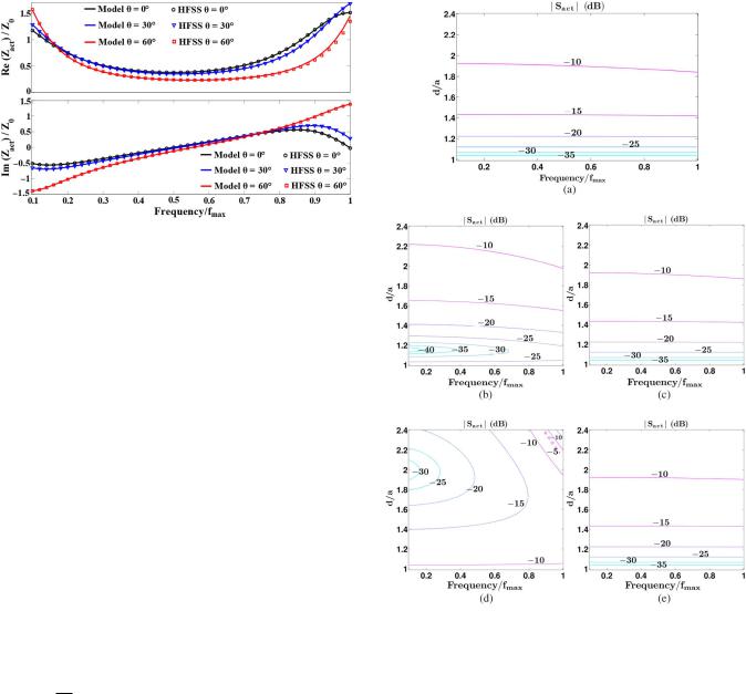
For standard applications, CTS arrays work in mono-modal regime. Thus, the slot width a must be lower than the cutoff wavelength λc of the first higher order mode propagating in the PPWs, i.e., λc = c/(2fmax√ r1), where fmax is the maximum frequency in the operating band. Given this constraint, a can be selected taking into account several design specifications. Here, we focus on the input matching. It generally improves for larger values of the aperture width a. The ratio between array spacing and slot width controls most of the performance of CTS arrays. The fast computation procedure proposed allows for an easy optimization of this parameter. Indeed, Sact can be mapped for several values of d/a, within a given frequency range and for different scan angles in E- and H-planes. Then, the value of d/a that best fits the requirements on Sact in terms of bandwidth and scanning range is selected. This process is illustrated for a CTS array fed by hollow PPWs and radiating in air, with a slot width a = 0.25 c/fmax. The contour plots of |Sact| as a function of d/a and frequency are shown in Fig. 4, for different scan angles. For broadside operation, the flat contour lines indicate the great stability of Sact over the decade considered. The best input matching is achieved for d ≈ a. As opposed to classical arrays, CTS antennas exhibit the widest bandwidths when the elements are tightly coupled. The results in Fig. 4(b)–(e) highlight different behaviors when the array beam is steered in the principal planes. In E-plane, the optimum ratio d/a for best matching varies with
Fig. 4. Contour plots of the amplitude of the active reflection coefficient Sact, as a function of frequency and ratio d/a, for different scan angles in E- and H- plane. (a) Broadiside. (b) E-plane, θ = 30◦. (c) H-plane, θ = 30◦. (d) E-plane, θ = 60◦. (e) H-plane, θ = 60◦.
the scan angle. Moreover, the return loss and bandwidth reduce for increasing angles. By contrast, |Sact| is almost frequency-independent and unaffected by the H-plane scanning. Thus, the ratio d/a selected for broadside operation allows for a wide-angle impedance matching in H-plane. With reference to the case discussed, a return loss >15 dB within a ±60◦ scanning range in both planes is achieved up to 0.6fmax by choosing d/a ≈ 1.4. The procedure can be iterated for different values of a, if wider bandwidths are targeted.
B. Largely Spaced CTS Arrays
The requirement for wide-angle scanning usually limits the element spacing and thus the size of the elements. In standard wide-scanning planar antennas, elements are arrayed in a double-meshed grid with periods close to half the wavelength at fmax, in order to avoid grating lobes. Such low inter-element spacings typically reduces the bandwidth of the array.
By contrast, CTS arrays suffer from grating lobes only when scanning in E-plane but not in H-plane. Indeed, the radiating elements

3296 |
IEEE TRANSACTIONS ON ANTENNAS AND PROPAGATION, VOL. 63, NO. 7, JULY 2015 |
Fig. 5. Active reflection coefficient versus scan angle in H-plane (solid lines) and E-plane (dashed lines) for several element spacings d. The slot width is a = 0.25λ, where λ is the free-space wavelength at the frequency considered. The CTS array is fed by hollow PPWs and radiates in free-space.
along H-plane are continuous slots of infinite length, or much longer than the wavelength in real cases. The presence of grating lobes can be detected from peaks in the amplitude of the active reflection coefficient. Fig. 5 reports |Sact| at fmax as a function of scan angle, both in E- and H-plane, for the CTS arrays studied in Section IV-A (a = 0.25 λmin). Several array spacings d are considered. The sharp maxima in E-plane for d > 0.5λmin indicate grating lobes centered in the corresponding angles. Conversely, Sact has small variations with the scan angle in H-plane, even for large values of d. The low matching level, due to large d/a, is not a concern since we are interested in the flatness of |Sact| against the scan angle. These results demonstrate that if CTS arrays are designed for H-plane scanning only, the active impedance is extremely stable against the beam pointing direction and almost frequency independent over a decade range. Since no grating lobes occur, a value of d > 0.5λmin can be chosen, thus reducing the number of slots and related transmitters/receivers (TXs/RXs). The slot width a can be increased up to the cutoff wavelength of higher order PPW modes to maximize matching level and bandwidth.
Few antennas exhibit such broadband, wide-angle scanning performance. Among them, connected arrays [7], [8] allow for twodimensional (2-D) scanning, but require element spacings <0.5λmin [8]. Thus, the number of feeds in a H-plane scanning CTS array of N slots is scaled down at least by a factor N, as compared to connected arrays of N elements, fed by a N × N network. A further reduction is achieved if the CTS antenna is designed with d > 0.5λmin.
C. Dielectric Cover for Wide-Angle Matching
A common way to improve the impedance matching of phased arrays over wide scan and frequency ranges consists in adding dielectric layers over the radiating apertures [16]. An easy case is here discussed for a CTS array whose PPW feeds are filled by a dielectric of relative permittivity r1 = 3.5. The slot width is a = 0.42 c/(fmax√ r1) and d = 1.4 a. A single-layer dielectric sheet of the same material used in the PPWs is placed just above the slots ( r2 = 3.5). Fig. 6 compares the VSWR at fmax of the unloaded CTS array to the ones computed for several thicknesses h of the cover. Without the cover, the array is mismatched (VSWR > 2) for every scan angle in H-plane and up to an angle of 50◦ in E-plane. When a 0.3λg-thick layer is added, a good matching is achieved up to 50◦ for both E- and H-scanning. Also the matching bandwidth is greatly improved. The unloaded array is mismatched in the band (0.1fmax, fmax) both in E- and H-plane, when the scan angle is 30◦. If the 0.3λg-thick cover is considered, a V SW R < 2 is achieved in
Fig. 6. VSWR in E- and H-planes at fmax for different thicknesses h of the dielectric cover, with r2 = 3.5, λg√= c/( r2 fmax). The CTS array analyzed (see Fig. 1) has a = 0.42 c/(fmax r1), d = 1.40 a, r1 = 3.5.
the bands (0.4fmax, fmax) and (0.6fmax, fmax) for E- and H-plane scannings, respectively.
V. CONCLUSION
A rigorous model for the analysis and design of parallel-fed CTS arrays has been presented. An accurate formula for the active impedance has been derived through a modal expansion of the magnetic currents over the slots. This approach provides results in excellent agreement with full-wave simulations even when few modes are considered. The impact of the array features on the bandwidth has been discussed. Some design procedures to achieve broadband, wideangle operation have been demonstrated through examples. This study proves that array spacings larger than half the minimum wavelength do not cause grating lobes nor significant bandwidth reduction for H-plane scanning.
REFERENCES
[1]N. T. Nguyen et al., “Design and characterization of 60-GHz integrated lens antennas fabricated through ceramic stereolithography,” IEEE Trans. Antennas Propag., vol. 58, no. 8, pp. 2757–2762, Aug. 2010.
[2]Y. Miura, J. Hirokawa, M. Ando, Y. Shibuya, and G. Yoshida, “Doublelayer full-corporate-feed hollow-waveguide slot array antenna in the 60GHz Band,” IEEE Trans. Antennas Propag., vol. 59, no. 8, pp. 2844– 2851, Aug. 2011.
[3]M. Ettorre, R. Sauleau and L. Le Coq, “Multi-beam multi-layer leakywave SIW pillbox antenna for millimeter-wave applications,” IEEE Trans. Antennas Propag., vol. 59, no. 4, pp. 1093–1100, Apr. 2011.
[4]W. W. Milroy, “The continuous transverse stub (CTS) array: Basic theory, experiment, and application,” in Proc. Antenna Appl. Symp., Sep. 25–27, 1991, vol. 2, pp. 253–283.
[5]W. W. Milroy, “Continuous transverse stub element devices for flat plate antenna arrays,” U.S. Patent 5 483 248, Jan. 9, 1996.
[6]W. W. Milroy, “Antenna array configurations employing continuous transverse stub elements,” U.S. Patent 5 412 394, May 2, 1995.
[7]A. Neto and J. J. Lee, “Ultrawide-band properties of long slot arrays,” IEEE Trans. Antennas Propag., vol. 54, no. 2, pp. 534–543, Feb. 2006.
[8]A. Neto, D. Cavallo, G. Gerini, and G. Toso, “Scanning performances of wideband connected arrays in the presence of a backing reflector,” IEEE Trans. Antennas Propag., vol. 57, no. 10, pp. 3092–3102, Oct. 2009.
[9]D. Cavallo and A. Neto, “A connected array of slots supporting broadband leaky waves,” IEEE Trans. Antennas Propag., vol. 61, no. 4, pp. 1984–1994, Apr. 2013.
[10]J. P. Doane, K. Sertel, and J. L. Volakis, “A wideband, wide scanning tightly coupled dipole array with integrated balun (TCDA-IB),” IEEE Trans. Antennas Propag., vol. 61, no. 9, pp. 4538–4548, Sep. 2013.

IEEE TRANSACTIONS ON ANTENNAS AND PROPAGATION, VOL. 63, NO. 7, JULY 2015 |
3297 |
[11]W. H. Henderson and W.W. Milroy, “Wireless communication applications of the continuous transverse stub (CTS) array at microwave and millimeter wave frequencies,” in Proc. IEEE/ACES Int. Conf. Wireless Commun. Appl. Comput. Electromagn., Apr. 3–7, 2005, pp. 253–256.
[12]A. Lemons et al., “W-band CTS planar array,” in Proc. IEEE MTT-S Int. Microw. Symp. Dig., Jun. 13–19, 1999, vol. 2, pp. 651–654.
[13]R.-S. Chu, “Analysis of continuous transverse stub (CTS) array by Floquet mode method,” in Proc. IEEE Antennas Propag. Soc. Int. Symp., Jun. 21–26, 1998, vol. 2, pp. 1012–1015.
[14]M. F. Iskander, Z. Yun, Z. Zhang, R. Jensen, and S. Redd, “Design of a low-cost 2-D beam-steering antenna using ferroelectric material and CTS technology,” IEEE Trans. Microw. Theory Tech., vol. 49, no. 5, pp. 1000– 1003, May 2001.
[15]L. B. Felsen and N. Marcuwitz, Radiation and Scattering of Waves. Hoboken, NJ, USA: Wiley/IEEE Press, 1994.
[16]E. Magill and H. A. Wheeler, “Wide-angle impedance matching of a planar array antenna by a dielectric sheet,” IEEE Trans. Antennas Propag., vol. 14, no. 1, pp. 49–53, Jan. 1966.
Tunable 3-D Bandpass Frequency-Selective Structure With
Wide Tuning Range
X. G. Huang, Z. Shen, Q. Y. Feng, and B. Li
Abstract—A new three-dimensional (3-D) tunable bandpass frequencyselective structure (FSS) with wide tuning range is presented. The tunable FSS consists of a periodic array of printed circuit boards and a number of inserted metallic plates, where varactor-loaded λ/4 stepped-impedance resonators (SIRs) are constructed based on the propagation mode excited in the structure. By properly choosing the impedance ratio of the SIRs, a wide tuning range can be achieved. Detailed discussion is given to determine the key parameters involved in this tunable FSS, including varactor-loaded λ/4 resonators and coupling coefficient. Finally, a prototype tunable FSS is fabricated and measured. The results exhibit a 2:1 (65%) frequency tuning range from 1.4 to 2.75 GHz with an insertion loss of 4.5–1.0 dB within the passband.
Index Terms—Stepped-impedance resonator (SIR), tunable frequencyselective structure (FSS), varactor diode.
I. INTRODUCTION
Tunable frequency-selective surfaces attracted great interest in recent years as tunable filters for multiband reflector antennas, for tunable radar absorbers, or to provide a varying transmission window in radomes [1]. Generating a dynamic frequency behavior requires the reactive characteristics of the surface to change with a tuning voltage, biasing magnetic field, or changing shape. Thus, the
Manuscript received August 05, 2014; revised February 10, 2015; accepted April 25, 2015. Date of publication May 01, 2015; date of current version July 02, 2015. This work was supported by the National Natural Science Foundation of China (NSFC) under Grant 61271090.
X. G. Huang and Q. Y. Feng are with the School of Information Science and Technology, Southwest Jiaotong University, Chengdu 610031, China (e-mail: xiaoguohuang@swjtu.edu.cn; fengquanyuan@swjtu.edu.cn).
Z. Shen is with the School of Electrical and Electronic Engineering, Nanyang Technological University, Singapore 639798 (e-mail: ezxshen@ntu.edu.sg).
B. Li is with the School of Electronic Science and Engineering, Nanjing University of Posts and Telecommunications, Nanjing 210003, China.
Color versions of one or more of the figures in this communication are available online at http://ieeexplore.ieee.org.
Digital Object Identifier 10.1109/TAP.2015.2428737
literature concerning tunable frequency-selective surfaces can be generally classified into three categories: mechanically tunable surfaces, magnetically tunable surfaces, and electronically tunable surfaces. Mechanically tunable frequency-selective surfaces are realized by changing the shape of its elements [2]–[4]. The elements can be either solid state [2] or liquid state [3], [4]. The magnetically tunable FSSs are implemented by using a ferrite substrate [5]. The permeability of the ferrite substrate can change with the external bias magnetic field. Although the magnetically and mechanically tunable FSSs do not need bias circuits, they suffer from several disadvantages, i.e., low tuning speed and small tuning range. The electronically tunable frequency-selective surfaces can be realized through conventional methods including loading with active semiconductor devices like varactor diodes [6]–[10], p-i-n diode [11], or barium-strontium-titanate (BST) varactor [12] in the element design. Although the electronic tuning requires the biasing circuit for electronic devices, it has many benefits, i.e., small size, nanosecond tuning speed, and low cost. Thus, the electronic tunable surfaces were widely studied in the past few years.
Recently, a novel concept of three-dimensional (3-D) frequencyselective structure (FSS) consisting of a two-dimensional (2-D) periodic array of vertical microstrip line resonators was reported in [13]–[15], where multiple transmission zeros/poles can be produced by a 3-D FSS with multimode cavities/resonators. Compared with 2-D surfaces, 3-D FSSs have demonstrated greater flexibility, better filtering performance, and stable angular response.
In this communication, a new second-order 3-D tunable bandpass FSS using varactor diodes is presented. This structure is based on 2- D periodic array of vertical varactor-loaded microstrip line resonators and a number of horizontal metallic plates. The proposed varactorloaded λ/4 stepped-impedance resonator (SIR) is first theoretically analyzed to demonstrate its superior performance in implementation of a wide tuning range. Design parameters of the via hole and metallic plate are then properly selected to meet the requirement of bandwidth and location of transmission zeros. Finally, a prototype 3-D tunable bandpass FSS with 2:1 (1.4–2.75 GHz) tuning range is fabricated and measured to verify our design concept and its tuning performance.
II. DESCRIPTION AND ANALYSIS OF THE TUNABLE FSS
The proposed tunable bandpass FSS, illustrated in Fig. 1(a), consists of an array of printed circuit boards and a number of inserted metallic plates and varactor diodes. Fig. 1(b) shows the detailed biasing circuit of the individual varactor diode consisting of an RF choke and a dc-blocking circuit. Fig. 1(c) and (d) shows the structural details of a unit cell, where the dash lines represent the periodic boundary. It is seen that two adjacent varactor-loaded λ/4 SIRs are coupled with each other through a via hole. In addition, a metallic plate of thickness t is inserted in the middle of the air gap formed by the microstrip line and the upper ground, which is used to realize a bandpass filtering response by blocking the air propagation path [14]. Periods along the x- and y-axes are denoted by b and h, respectively. The thickness of proposed tunable FSS along the z-axis is represented by l. D denotes the diameter of via hole.
In this structure, two quasi-TEM modes are excited in the shielded microstrip resonator: air mode and substrate mode [14]. The substrate mode mainly contributes to the passband of the tunable FSS, whereas the air mode only influences the out-of-band rejection. Thus, the passband and stopband can be independently controlled by substrate mode and air mode, respectively. When the E-field of an incident plane wave is perpendicular to the strips (TE-polarization), as indicated in Fig. 1, the varactor-loaded SIR-based structure will exhibit a tunable
0018-926X © 2015 IEEE. Personal use is permitted, but republication/redistribution requires IEEE permission. See http://www.ieee.org/publications_standards/publications/rights/index.html for more information.