

диафрагмированные волноводные фильтры / fe74d354-96c9-46b7-b0d8-b24457fe94af
.pdfSubstrate
Integrated
Waveguide Filter
Xiao-Ping Chen and Ke Wu
|
licensed |
by |
Image |
|
|
|
|
Ingram
The electromagnetic (EM) spectrum is becoming more crowded, and it is densely populated with various wireless signals and parasitic interferers in connection with communication and sensing services. Increasingly sophisticated
radio-frequency (RF), microwave, and millimeter-wave filters are required to enable the selection and/or rejection of
|
specific frequency channels. This will occur in future gen- |
||
|
erations of the wireless system, such as the current hotly |
||
|
debated fifth-generation communication systems, where |
||
|
the spectral channelization of a heterostructured wide- |
||
|
|
band signals will be critical in support of a host of coex- |
|
|
|
isting bandwidths or speeds and applications. Bandpass |
|
|
|
filters have been the most useful and popular types for |
|
|
|
such applications and are the most difficult to design |
|
|
|
|
and develop in practice. Other types of filters such as |
|
|
|
notch (stopband) and lowpass filters have also been |
|
|
|
widely used in many systems, and their design is |
|
|
|
generally perceived less critical with respect to band- |
|
|
|
pass filters. This article will focus on the presenta- |
|
|
|
tion and discussion of bandpass filters. Design fac- |
|
|
|
tors or parameters of filters, such as selectivity, cost, |
|
|
|
miniaturization, sensitivity to environmental ef- |
|
|
|
fects (temperature and humidity, for example), and |
|
|
|
power handling, combined with predefined in- |
Publ |
|
|
band and out-of-band performance metrics, are |
ing |
critical specifications of the design with respect |
||
ish |
|
|
|
to the development of RF and microwave front
Xiao-Ping Chen and Ke Wu (ke.wu@polymtl.ca) are with the Poly-Grames Research Center, Department of Electrical Engineering, École Polytechnique (University of Montreal), Center for Radiofrequency Electronics Research of Quebec, Montreal, Canada.
Digital Object Identifier 10.1109/MMM.2014.2321263
Date of publication: 11 July 2014
108 |
1527-3342/14©2014IEEE |
July/August 2014 |

ends. This is indispensable for the efficient utilization of frequency spectrum resources and the cost-effec- tive enhancement of wireless system performances.
Basic Filter Design Considerations and Challenges
The designer may often be required to make a compromise between several conflicting requirements since it is rather difficult or even physically and/or electrically impossible to simultaneously satisfy some design criteria or specifications. For example, achieving higher channel selectivity usually requires, to the first order, the use of more resonators, which will in turn result in a higher insertion loss along the transmission path because the insertion loss is approximately proportional to the number of resonators used in the construction of a filter. A bandpass filter made of resonating elements such as cavities requires a number of high unloaded quality factor ^Quh resonators for maintaining low insertion loss and hence minimum noise figure. The unloaded quality factor of a resonator at microwave frequencies is generally proportional to its volume and also its cost. This is closely related to the mode of resonance (field profiles within the structure) and the quality of material, which will be detailed below. There is always a tradeoff between performance requirements and development costs in filter design and construction.
The loss mechanism of a resonating building block is not only closely related to such physical and electrical parameters as thickness, material, shape, dielectric loss, conductor loss, leakage loss, and radiation loss but also to the resonant-mode behavior. A specific resonance behavior is directly related to the electric and magnetic field distribution of such a mode inside the structure, which is responsible for the loss mechanism. The electric and magnetic fields are normally connected to the dielectric and conducting losses, respectively, if the structure is not subject to any leakage and radiation losses. The choice of a particular operating mode could yield a different performance but often the choice is quite limited. A resonator can support multiple resonant modes, depending on the mechanism of excitation, the shape of the structure, and the frequency of resonance. Multimode resonators can also be used to reduce the number of resonating building blocks required for the number of electrical resonances and, as a result, the insertion loss and the filter size can be reduced. The most well-known examples are the dual-mode and triple-mode resonators and filters. There is always a requirement on the development of appropriate resonating building blocks for a
July/August 2014
good tradeoff between cost and loss in the design of a bandpass filter.
The design and development of a high-quality filter is closely related to the choice of an appropriate trans- mission-line or waveguide technology. Depending on a specific frequency range of interest and the relative frequency bandwidth of application, either a metallic waveguide, coaxial line, planar structure, or a hybrid form of those different geometries can be used. Different hardware technologies present different electrical and physical features and characteristics, which have direct impact on the performance, size, and cost of the filter. Different transmission lines can support different types of mode [transverse electromagnetic (TEM) mode or non-TEM mode, for example] that can fundamentally determine the filtering features. Nonplanar metallic waveguides in the form of rectangular and/ or circular shapes are bulky and costly, and are usually selected for high-performance, loss-sensitive, and high-power driven design. Printed or etched planar transmission lines have been widely used for low-cost applications that demand high-density integration and small size or form factor. They have relatively high losses and are subject to some serious packaging issues because of their semiunbounded or unbounded geometry. Conventional and microcoaxial line technologies, which are also nonplanar and relatively expensive to design, present a certain degree of compromise between the waveguide and planar structures based on the design and application requirements; however, they cannot be used for the purpose of integration. The most critical challenge in the use of nonplanar structures for filter design is that it is always challenging to integrate active devices with such filters as the associated transitions present added transmission loss, design complexity, and production cost.
The use of high-performance metallic waveguides is highly desirable if high-quality factors must be considered in the filter design. Such a high-Q preference is always the ideal scenario in any filter development. The integrability of low-profile planar structures provides a unique and attractive solution for mass-pro- duction or cost-sensitive applications, even though their Q-factor is undesirably low. The fusion or blending of planar and nonplanar structures in some manner definitely presents the best compromise judging from performance, cost, size, manufacturability, and many other aspects. This has led to the emergence and development of the concept of substrate integrated circuits (SICs) [1] in which any nonplanar structure may organically be synthesized into planar form that makes itself compatible and/or integrable with other planar
109

circuits, and amenable to nearly any planar processing technique. The planarization of nonplanar structures is readily made possible thanks to the rapid development of low-cost microfabrication techniques with respect to vertical interconnects and substrate processing such as via developments and hole formations.
The SICs scheme provides a variety of integration scenarios and topological interconnects, such as the presently popular substrate integrated waveguide (SIW), which can be made together on the same dielectric substrate with other planar circuits. This context of substrate integration has been involving all aspects of SIW technology in recent years, from the development of the SIW technique and its applications to the design and development of innovative filters.
This article presents a comprehensive review of SIW filter technology. Special emphasis is placed on the current status of research and development as well as the future outlook of this emerging technology in connection with various applications.
Design Guideline and Fundamental Properties of SIW
As mentioned earlier, an SIW is a synthesized nonplanar waveguide transformed into planar form, which can then be integrated into any planar dielectric substrate with any planar fabrication or processing technique including printed circuit board (PCB), and low-temperature cofired ceramic (LTCC) technologies, among others. This emerging guided-wave structure can be made with a pair of periodic metalized via arrays or slot trenches and it looks like two parallel fences that have a specific spacing in which EM waves are well confined, as depicted in Figure 1.
The SIW scheme belongs to the family of SICs in which any other nonplanar structures such as dielectric waveguides and coaxial lines can also be made in planar form [1]. Since the truncated side walls do not allow longitudinal current flow, the SIW structure only supports the propagation of quasitransverse electric (TE) modes that have properties similar to
Top Metal  Substrate
Bottom Metalized |
w: Width of SIW |
Metal Via Hole p |
weff: Width of Rectangular |
d |
Waveguide |
w d: Diameter of Metalized |
|
|
Via Hole |
|
|
|
p: Pitch Between Adjacent |
|
Via Hole |
Figure 1. An SIW and its equivalent rectangular waveguide (from [1]).
110
those in a conventional metallic waveguide. In most cases, only the TEm0 modes are of interest because the substrate thickness is relatively thin with respect to the SIW width (at least twice). If generated or existing along the structure, transverse magnetic (TM) modes will immediately become leaky through unbounded via windows along the transversal direction. In the design of E-plane discontinuities, one must ensure that the SIW structure does not present strong leakage losses. The absence of TM modes creates a very favorable condition for the bandpass filter design because certain mode problems, which may be responsible for out-of-band parasitic responses, can be avoided. This is a distinct feature of the SIW technique for filter design.
Various wave guidance and leakage characteristics of the SIW were discussed in detail in [2] and [3]. In the design of SIW components, one must ensure that the SIW operates in the frequency band of interest where there are no bandgap effects and leakage loss is negligible over the entire waveguide bandwidth of interest. The SIW is a periodic structure, always subject to bandgap phenomena. The frequency region of interest for the SIW is drawn and described in Figure 2. When the period length increases, the EM field may no longer be confined within the two arrays of via cylinders. Part of the energy may also propagate outside the two rows of cylinders, thus resulting in leakage losses. The bandwidth of the bandgap increases when the diameter of the cylinder decreases. Furthermore, half of the bandgap may appear inside the single-mode operation bandwidth [3]. The TE10 -mode related frequency region of interest is defined by
p 2 d |
(1a) |
||
p/mc 1 |
0.25 |
(1b) |
|
al /k0 |
1 |
1 # 10-4 |
(1c) |
p/mc |
2 |
0.05, |
(1d) |
where al is the total loss and k0 is the wave number in free space. The condition (1a) states that the period length must be larger than the cylinder diameter so that the circuit is physically realizable, and (1b) is required to avoid any bandgap in the operating bandwidth of TE10 mode and other related guided-wave modes if involved. To be negligible, the leakage losses must respect (1c). A more restrictive and general condition for negligible leakage losses is p # 2d. Finally, a nonessential but desirable condition for the manufacturing process is to have d comparable to the substrate thickness. These via cylinders are usually mechanically drilled and chemically electroplated or plasmadeposited, and the production time is directly related to the choice of a processing technique. If the length of the period is very small with respect to the guidedwave wavelength, the mechanical rigidity is adversely affected. The number of cylinders should therefore not exceed 20 per wavelength, as stated in (1d).
July/August 2014

|
0.3 |
|
Bandgap Region |
|
|
|
|
|
0.25 |
|
|
|
|
Leakage |
|
|
0.2 |
Region |
Region of |
c |
|
|
Interest |
0.15 |
|
|
|
/m |
|
|
|
p |
|
|
|
|
0.1 |
|
Unrealizable |
|
|
Region (d >p) |
|
|
|
|
0.05Overperforated
00 |
|
Region |
|
|
|
|
0.05 |
0.1 |
0.15 |
0.2 |
0.25 |
0.3 |
d/mc
Figure 2. The region of interest for the SIW in the plane of d/mc, p/mc (from [3]).
A set of basic but empirical design rules that allow an appropriate choice of various physical parameters such as the cylinder diameter and the period length as a function of the desired cutoff frequency is given in
(1) [3]. A more rigorous design process may be required for precision SIW circuits. Those basic design rules provide a good guideline for the designer to choose appropriate structural parameters.
In the TE10 -mode frequency region of interest, the SIW is equivalent to a conventional rectangular waveguide that has negligible leakage losses and does not present any bandgap in its operating bandwidth. The physical meaning of such an equivalence is that the real SIW and its equivalent dielectric-filled rectangular metallic waveguide share the same TE10 mode cutoff frequency and related dispersion properties. A simple static equivalent width of the SIW is given approximately by [4]
weff = w - |
d2 |
, |
(2) |
|
0.95p |
||||
|
|
|
provided that p is sufficiently small. A more accurate empirical equation is proposed as follows:
weff = w - 1.08 # |
d2 |
+ 0.1 # |
d2 |
, |
(3) |
|
p |
w |
|||||
|
|
|
|
when p/d is smaller than 3 and d/w is smaller than 1/5. For high-order TEm0 modes of the SIW, the dispersion characteristics are also the same as its equivalent rectangular counterpart. However, there is a subtle difference in the equivalent width between the highorder modes and the fundamental mode [2]. This involves more numerical calculations and analysis.
In this way, the quasi-TE modes of SIW (TE10 mode, in particular) can effectively be mapped into the standard dielectric-filled TE waveguide modes with continuous metallic side walls through an equivalent
Table 1. Comparison of the Q-factor of SIW with respect to that of 50-X microstrip line and standard waveguide at Ka-band (from [5]).
Properties |
Microstrip1 (50 X) |
SIW1,2 |
Waveguide |
Q-factor |
42 |
462 |
4,613 |
1Substrate: fr = 2.33, tan d = 5 # 10-4, h = 10 mils, copper roil 2Width = 200 mils
waveguide width that determines the cutoff frequency. Existing design models, analysis equations, and synthesis tools associated with rectangular waveguide circuits can be deployed in a straightforward manner for the development of SIW components, circuits, and systems. A large number of passive and active SIW components have been successfully designed and demonstrated, including couplers, dividers, filters, oscillators, mixers, and amplifiers. In some cases, full-wave field simulations and optimizations may be needed to validate and adjust (tune) the SIW circuit layouts in conjunction with such design approaches. This is often required for special scenarios such as millimeter-wave, high-Q, narrowband, tolerance-sen- sitive, and multiple-element coupled SIW integrated circuits and components.
In the development of RF, microwave, and mil- limeter-wave filters, transmission loss is one of the most crucial design considerations and influences the choice of materials and structures. The loss of SIW structures mainly comes from dielectric and conductor losses because the SIW geometry is self-packaged and not subject to radiation loss. The total transmission loss, inferred from the Q-factor of transmission lines or circuits, increases as frequency increases. This loss increase is also related to the decreasing thickness of substrate and surface roughness, which is becoming electromagnetically visible. The surface roughness should be taken into account at higher millimeterwave frequencies and terahertz. The electrical and mechanical quality of via holes and metal plating is also critical to this loss effect, which is often difficult to characterize. Table 1 shows the typical Q-factor of SIW transmission lines at Ka-band compared with that of a 50-X microstrip line and an air-filled standard rectangular waveguide without sophisticated polishing and plating. An SIW fabricated by a low-cost PCB process has a Q-factor significantly larger than that of a low-cost microstrip line, but lower than that of a costly and bulky standard waveguide. This comparison clearly shows that an SIW presents an excellent tradeoff between loss and cost, which is the foundation for low-cost, high-quality filter design with this emerging technology. The SIW presents an outstanding tolerance of fabrication, which will be discussed in one of the companion articles to be published in upcoming issues of IEEE Microwave Magazine.
July/August 2014 |
111 |

SIW Resonator
The SIW has recently become very popular for the design and development of high-performance and cost-sensitive filters over a very large frequency range from subgigahertz to subterahertz. Why are the SIW techniques so attractive for the filter community and why can they do better than their counterparts? The advantage of a reduced loss cannot be the sole reason.
To answer this question, let us first look at the basic quality-defining parameters of filters. Figure 2 shows the relative insertion loss, size, and cost of typical microwave resonators made by different techniques. Note that those resonators are the building blocks of filters. The estimated range of unloaded quality ^Quh values for each category of resonator at 5 GHz (with an SIW cavity resonator at 30 GHz made of a general PCB substrate) is also given in the same figure to illustrate their differences. The Qu value can vary widely for each category due to the fact that there is a wide range of resonator configurations that can be chosen under each category of resonator. For example, a patch microstrip resonator would have a higher Qu value than a standard half-wavelength resonator, and a full-height TE101 waveguide cavity would have a higher Qu than a heightreduced TE101 waveguide cavity resonating at the same frequency [6]. The choice of a dielectric substrate is also critical to the Qu value, as loss tangent characteristics are different from one material to another.
For a given resonator, different excitations may generate different modes that also may have different Qu values. This is because a different mode has a different field pattern and current distribution over the structure of
interest, leading to a different loss mechanism in connection with the conducting surface and dielectric volume. A TE101 cavity, for example, can also support the resonance of a TE102 cavity, which has different field patterns and current distributions. Therefore, the Qu values for those two modes within the same cavity should be different.
From Figure 3, the Qu of a microstrip line or stripline resonator is fundamentally limited by system losses, rendering them inadequate for many applications even though the microstrip or stripline filter technology offers a low-cost solution with a small footprint and integrated geometry. When a high selectivity is required, dielectric resonator or metallic waveguide technology is preferred. While this type of technology offers a very high unloaded quality factor in the range of thousands and beyond, their size and weight make them prohibitive in many practical applications. In addition, they are much more costly than the printed circuit or planar counterparts [6]–[8]. This filter-related statement on the loss and cost aspects is also consistent with the analysis and explanation made in the beginning of this article regarding various planar and nonplanar transmission lines.
The recent widely studied SIW technology is able to fill the technological gap between microstrip or stripline (planar type) and dielectric resonator or metallic waveguide (nonplanar type), since it combines the best parts of both and offers high-quality factors that are close to those of nonplanar structures with the sizeand costrelated advantages of printed planar circuits. The Qu value of an SIW cavity resonator is determined by three Q values: a conduction quality factor, Qc, related to lossy conducting walls, a dielectric loss quality factor, Qd, and
Loss
Half-Wavelength |
|
|
|
Patch |
Q = 50 ~ 200 |
|
|
|
|
Qu = 150 ~ 1,000 |
|
|
Microstrip |
Qu = 200 ~ 3,000 |
|
|
/Stripline |
Qu |
= 1,000 ~ |
|
|
SIW |
12,000 |
|
|
|
|
|
|
Dielectric |
|
|
|
Resonator |
|
|
Super- |
Waveguide |
|
|
|
Size |
|
|
conductor |
|
|
Figure 3. The relative insertion loss, size, and cost of various RF resonators [6], [7].
112 |
July/August 2014 |

Microstrip
Substrate
Via Holes
Center Coupling |
Offset Coupling |
Double Coupling |
Quadrature Coupling |
Figure 4. Various exciting topologies of SIW cavity resonators with microstrip lines as inputs and outputs (from [9]).
a leakage quality factor, Ql, representing energy leakage from the periodic structure via gaps. When certain geometrical design conditions presented in (1) are satisfied with respect to the operating frequency range, the power loss caused by leakage is much smaller than the dissipated power on metallic surfaces and in dielectric substrate. The conduction and dielectric loss mechanisms have the dominant effect on the Qu of an SIW cavity resonator. For general and practical PCB dielectric substrates and ceramic substrates of various thickness, the Qu of an SIW cavity resonator may be in the range of 150 + 1, 000. Higher values are possible with low-loss substrates such as quartz and processed metallic surfaces such as gold-plating. The overall fabrication cost of SIW circuits is slightly higher than that of microstrip counterparts, because a large number of metalized via holes or slot trenches are needed in the SIW circuits.
Figure 4 shows various exciting topologies for SIW cavity resonators. The corresponding Qu on a low-cost commercial PCB substrate of RT/Duroid 5880 with thickness of 0.508 mm is presented in Table 2. The coupling between the cavity and the planar transmission lines can be made with current probes when the cavity acts as a bandpass filter. The current probe is built by moving (or removing) via holes on one side of the cavity to make place for an insert. The strength of coupling of a current probe will mainly depend on the depth and width of the probe. The Qu can be calculated from the measured S-parameters as
Qu = |
Ql |
, |
(4) |
|||
1 - |
S21 |
|||||
where |
|
|
|
|
|
|
|
|
f0 |
|
|
(5) |
|
Ql = |
Df3 dB . |
|
||||
|
|
|||||
July/August 2014
Table 2. Comparison of the Qu-factor of SIW cavity resonators for various exciting topologies by using a 50-X microstrip (from [9]).
|
Resonator Frequency |
|
Exciting Topology |
of TE101 Mode |
Qu |
Center coupling |
21.430 GHz |
542 |
Double coupling |
21.118 GHz |
490 |
Quadrature coupling |
21.075 GHz |
414 |
1Substrate: fr = 2.2, tan d = 9 # 10-4, h = 20 mils, copper roil
To reduce effects in connection with the coupling loss, the coupling should be weak, meaning S21 1-10 dB. From the measured results, the best Qu of 542 can be obtained by the center coupling on a low-cost commercial PCB substrate [9]. As mentioned previously, the SIW structure does not support the propagation of TM modes because of discontinuous side walls that prevent the current from flowing. This is a very positive point for filter design, because the SIW filter should have fewer parasitic modes, and the fundamental mode bandwidth will generally be larger than its rectangular waveguide filter counterpart.
The hybrid integration of planar and nonplanar structures in SIW structures enables the design of filters with self-packaging features that can be used in the development of advanced packaging systems. This could resolve some well-known bottleneck problems of microwave and millimeter-wave interconnects and packaging [1], [10]. One of the most attractive features of SIW technology lies in its excellent repeatability for volume production when the design layout is made in the same manner as planar integrated circuits. With easily accessible and low-cost, high-precision planar fabrication techniques, SIW filters can be designed and processed without resorting to expensive and laborious postfabrication tuning such as in the case of conventional waveguide filters. This is critical for quick turn-around, high-volume and high-yield commercial applications.
We begin with examining the recently published results from research groups scattered around the world, highlighting different but mainstream and innovative filter topologies with state-of-the-art design technologies. Our own work is discussed, which deals with a wide range of filter design schemes. Interesting and useful schemes of miniaturization and practical aspects of SIW filters are addressed.
Thanks to the equivalence between via-hole walls and metallic walls for TEn0 ^n = 1,2,3fh modes [1], most of the filter topologies suitable for conventional metallic waveguides can be implemented directly on an SIW platform at very low cost. The hybrid integration of planar and nonplanar circuits on an SIW platform makes the SIW filter design much more flexible,
113
Top Metal
Substrate
Coupling Slot
|
S KIO’ {io r {12 K12’ {12 |
{45 K45’ {45 r{io KIO’ |
|
|
|
||
|
Bottom Metal |
|
|
50-X |
Metallized Via Hole |
|
|
Microstrip |
|
|
|
(a) |
(b) |
|
|
|
|
E Field (Y_Per_m)
5.5954e + 004
5.2457e + 004
4.8960e + 004
4.5463e + 004
4.1965e + 004
3.8468e + 004
3.4971e + 004
3.1474e + 004
2.7977e + 004
2.4480e + 004
2.0983e + 004
1.7486e + 004
1.3988e + 004
1.0491e + 004
6.9943e + 003
3.4971e + 003
1.2872e - 002
(c)
Figure 5. (a) A geometric configuration, (b) equivalent circuit, and (c) electrical field intensity distribution of a fifth-order direct-coupled SIW cavity filter with the first/last SIW cavity directly excited by 50-Ω microstrip lines (from [18]).
but at the same time increases the challenge in effectively designing an SIW filter. A wide array of innovative and creative SIW filter topologies and design techniques are being reported in the current literature over a very wide range of frequencies from subgigahertz to subterahertz. These SIW filters are made of various materials by different processing techniques.
Direct-Coupled SIW Cavity Resonator Filters
Direct-coupled waveguide resonator filters, of which waveguide cavities are cascaded by coupling iris on the common wall, can easily be made compatible with SIW technology [11]–[22]. An inductive iris is preferred for the realization of coupling in SIW filters because it has a better stopband performance with respect to an inductive post. Standard 50-X microstrip lines, striplines, or CPW structures can be used to excite the first/ last SIW cavity resonator directly by coupling slots [9]. Figure 5 shows the typical geometric configuration and equivalent circuit of a fifth-order direct-coupled SIW cavity resonator filter made of a PCB substrate. The electrical field intensity distribution at 20 GHz with 1-W input power, similar to that in a rectangular waveguide filter, is also shown.
When an iris is used without strong frequencydependent dispersion, the direct-coupled SIW cavity fil-
ter will exhibit a standard Chebyshev response whose mathematical approximation and circuit synthesis are well known. As for the dimensional synthesis, lengthy and global full-wave modeling-based tuning and optimization of the entire filter structure can be avoided (as proposed in [18]–[22]). This saves development cost and time as well as bypasses the tedious tuning procedure because of a large number of metalized cylindrical via holes used in the SIW structure. Note that the via-hole scheme is more popular than the slot trench counterpart because the fabrication accuracy of a via-hole array is better than that of a slot trench. The via-hole SIW structure is therefore considered in this article unless mentioned otherwise.
The classical theory [23], [24] for module design is an effective procedure for the dimensional synthesis of a direct-coupled SIW cavity filter. The generalized immittance inverter [24] should be used for the parameter extraction of input/output couplings, because different types of transmission lines are used on the two sides of immittance inverter. In addition, a realistic SIW structure rather than its equivalent rectangular waveguide model should be used for accurate parameter extraction of the postwall coupling iris and input/output coupling structures. The equivalent electrical length of the postwall iris and the input/output coupling structures has a
114 |
July/August 2014 |

|
|
|
|
|
|
|
|
|
R1 |
R2 |
|
|
|
|
|
|||||
|
|
|
|
|
|
|
|
|
|
|
|
|
|
|
|
|
|
P2 |
||
P1 |
Waveguide SIW |
|
SIW |
Waveguide |
||||||||||||||||
|
|
|
|
|
|
|
|
|
|
|
|
|
|
|
|
|
|
|
|
|
|
|
|
|
|
|
|
|
|
|
|
|
|
|
|
|
|
|
|
|
|
|
|
|
|
|
|
|
|
|
|
|
|
|
|
|
|
|
|
|
|
|
|
|
|
|
|
|
|
|
|
|
(a) |
|
|
|
|
|
|||||
|
P1 |
|
|
|
|
|
R1 |
|
|
|
|
|
|
R2 |
|
|
|
|
P2 |
|
|
|
|
Error |
|
|
DUT |
|
|
|
Error |
|
|||||||||
|
|
|
|
|
|
|
|
|
|
|
|
|
||||||||
|
|
|
|
|
|
|
|
|
|
|
|
|
|
|
|
|
||||
|
|
|
|
Box |
|
|
|
|
|
|
|
|
|
Box |
|
|
||||
|
|
|
|
|
|
|
|
|
|
|
|
|
|
|
|
|
|
|||
|
|
|
|
|
|
|
|
|
|
(b) |
|
|
|
|
|
|||||
|
P1 |
|
|
|
|
|
|
|
R1 |
R2 |
|
|
|
P2 |
||||||
|
|
|
|
Error |
|
|
|
|
|
|
|
|
|
|
Error |
|
||||
|
|
|
|
Box |
|
|
|
|
|
|
|
|
|
|
Box |
|
||||
|
|
|
|
|
|
|
|
|
|
(c) |
|
|
|
|
|
|||||
|
|
|
|
|
|
|
|
|
|
|
|
|
|
|
||||||
|
P1 |
S11R |
|
R1 |
R2 |
|
S22R P2 |
|||||||||||||
|
|
|
|
Error |
|
|
|
|
|
|
|
|
|
|
Error |
|
||||
|
|
|
|
|
|
|
|
|
|
|
|
|
|
|
||||||
|
|
|
|
Box |
|
|
|
|
|
|
|
|
|
|
Box |
|
||||
|
|
|
|
|
|
|
(d) |
|
|
|||||||||||
|
|
|
|
|
|
|
|
|
|
|
|
|
|
|
||||||
|
|
|
|
|
|
|
|
|
|
|
|
|
|
|
||||||
|
P1 |
|
|
|
|
|
R1 |
|
|
l |
|
|
|
R2 |
|
|
|
P2 |
||
|
|
|
|
Error |
|
|
|
SIW |
Error |
|
||||||||||
|
|
|
|
Box |
|
|
|
|
Box |
|
|
|||||||||
|
|
|
|
|
|
|
|
|
|
|
|
|
|
|||||||
|
|
|
|
|
|
|
|
|
|
|
|
|
|
|
|
|
|
|
|
|
(e)
Figure 6. Block diagrams of a numerical TRL calibration procedure for postwall iris (from [18]). (a) Postwall iris, (b) DUT, (c) through, (d) reflect, and (e) line.
significant influence on the resonator frequency of SIW cavity resonators.
Numerical calibration techniques such as TRL, whose procedure is described in Figures 6 and 7, present an efficient method for the accurate parameter extraction of SIW discontinuities [18]. These numerical calibration procedures, similar to the well-established experimental calibration techniques, are used to calibrate out port or connection discontinuity effects between the periodic SIW structures and reference lines. Potential numerical errors and theoretical modal approximations in the simulation could lead to serious problems in the parameter extractions for equivalent circuit models from the field computations. For typical parameter extractions, the reference lines may be set up in the form of a waveguide structure or microstrip line. This procedure is absolutely necessary when an accurate and one-pass design is anticipated.
Compared with the conventional metallic waveguide filter, the direct-coupled SIW cavity resonator filter has a wider stopband because the SIW structure
July/August 2014
|
R1 |
l1, l2 |
R2 |
|
P1 |
|
SIW |
|
P2 |
|
|
|
|
|
(a)
P1 R1

 Error
Error 
Box
DUT R2
I/O: 
 I/O:
I/O:
UstripSIW SIW-
SIW 
 Ustrip
l1, l2
(b)
P2
Error 

Box
Figure 7. Block diagrams of numerical TRL calibration procedure for input/output structure (from [18]). (a) Input P1/output and (b) DUT.
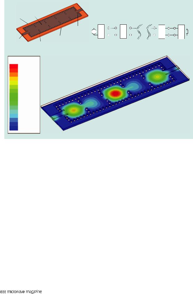
does not support the propagation of TM modes. The stopband performance can be improved by using symmetric excitation/coupling since odd-order modes cannot exist for symmetric coupling [9]. In addition, some novel techniques compatible with SIW schemes have been developed to further improve the performance of a direct-coupled SIW cavity resonator filter. In [25] and [26], the patterned transverse radiating slots at the proper positions of SIW cavities are used to effectively reject the second longitudinal resonant modes. Four cells of a slotted planar structure (SPS) are adopted on the top plane of the both input and output feed lines of the SIW filter to reject the undesired passbands. The fifth-order direct-coupled SIW cavity filter with a center frequency of 10 GHz and 10% frequency bandwidth is designed and manufactured on RT/Duroid 5870. The measurement results presented in Figure 8 show a wide stopband from 11 to 18 GHz below –30 dB.
The stepped-impedance resonator scheme, which stems from microstrip resonator, has been successfully used in the direct-coupled SIW resonator filter with a wide stopband [27], [28]. The stepped-impedance resonators implemented by H-plane discontinuities inherently have different spurious frequencies so the spurious passband can be degraded. On the other hand, the spurious resonance can be pushed to a higher frequency by selecting the appropriate length and impedance ratio of the resonator. The second resonance of the fundamental TE10 mode can be pushed to 1.5 f0 by using E-plane discontinuities to realize the stepped-impedance resonator, similar to the ridged SIW filter [29].
Conclusions
Basic structures and characteristics of SIW are presented and reviewed to highlight the attractiveness of this emerging technology. Design rules that are important for the development of SIW filters and other circuits are discussed. The SIW resonator is compared with other
115

|
|
|
|
|
|
|
|
|
|
|
|
[12] H. Leblond, J. F. Villemazet, J. L. Ca- |
|
|
|
|
|
|
|
|
|
|
|
|
|
||
|
0 |
|
|
|
|
|
|
|
|
|
|
zaux, D. Pacaud, J. J. Herren, L. Rigaud- |
|
|
|
|
|
|
|
|
|
|
|
|
eau, L. Lapierre, D. Baillargeat, P. Blon- |
||
|
|
|
|
|
|
|
|
|
|
|
|
||
|
-10 |
|
|
|
|
|
|
|
|
|
|
dy, S. Bila, S. Verdeyme, C. Delage, C. |
|
|
|
|
|
|
|
|
|
|
|
|
Quendo, J. F. Favennec, B. Potelon, E. |
||
|
|
|
|
|
|
|
|
|
|
|
|
Rius, F. Seyfert, and S. Pacchini, “When |
|
|
-20 |
|
|
|
|
|
|
|
|
|
|
new needs for satellite payloads meet |
|
|
|
|
|
|
|
|
|
|
|
|
with new filters architecture and tech- |
||
|
|
|
|
|
|
|
|
|
|
|
|
||
(dB) |
-30 |
|
|
|
|
|
|
|
|
|
|
nologies,” in Proc. European Microwave |
|
|
|
|
|
|
|
|
|
|
|
Conf., Rome, Italy, Sept. 29–Oct. 1, 2009, |
|||
|
|
|
|
|
|
|
|
|
|
|
|||
K |
|
|
|
|
|
|
|
|
|
|
|
pp. 1712–1715. |
|
-40 |
|
|
|
|
|
|
|
|
|
|
[13] M. Salehi and E. Mehrshahi, “A closed- |
||
21 |
|
|
|
|
|
|
|
|
|
|
form formula for dispersion character- |
||
S |
|
|
|
|
|
|
|
|
|
|
|
||
K.O |
-50 |
|
|
|
|
|
|
|
|
|
|
istics of fundamental SIW mode,” IEEE |
|
11 |
|
|
|
|
|
|
|
|
|
|
Microwave Wireless Compon. Lett., vol. |
||
OS |
-60 -1 |
|
|
|
|
|
|
|
|
Simulated S21 |
|
21, no. 1, pp. 4–6, Jan. 2011. |
|
|
|
|
|
|
|
|
|
|
|
[14] D. Deslandes and K. Wu, “Millimeter- |
|||
|
-5 |
|
|
|
|
|
|
|
|
Simulated S11 |
|
wave substrate integrated waveguide |
|
|
|
|
|
|
|
|
|
|
|
filters,” in Proc. IEEE Canadian Conf. |
|||
|
-70 |
|
|
|
|
|
|
|
|
Measured S21 |
|
Electrical Computer Engineering, Mon- |
|
|
-10 |
9.5 |
10 |
10.5 |
11 |
|
|
Measured S11 |
|
treal, QC, Canada, May 4–7, 2003, pp. |
|||
|
-80 |
|
|
|
|
1917–1920. |
|||||||
|
|
|
|
|
|
|
|
|
|
|
|||
|
8.5 |
9.5 |
10.5 |
|
11.5 |
|
12.5 13.5 |
14.5 15.5 |
16.5 17.5 18.5 19.5 |
|
[15] Z.-C. Hao, W. Hong, J.-X. Chen, X.-P. |
||
|
|
|
|
|
|
|
Frequency (GHz) |
|
|
|
Chen, and K. Wu, “Planar diplexer for |
||
|
|
|
|
|
|
|
|
|
|
microwave integrated circuits,” IEE |
|||
Figure 8. A photograph of the fabricated filter and simulated and measured results of the |
Proc. Microwaves, Antennas Propagat., |
||||||||||||
vol. 152, no. 6, pp. 455–459, Dec. 2005. |
|||||||||||||
fifth-order SIW filter with slots and SPS manufactured on RT/Duroid 5870 with a height of |
[16] T.-S. Yun, H. Nam, K.-B. Kim, and J.-C. |
||||||||||||
0.7874 mm (from [26]). |
|
|
|
|
|
|
|
|
Lee, “Iris waveguide bandpass filter |
||||
|
|
|
|
|
|
|
|
|
|
|
|
using substrate integrated waveguide |
|
microwave resonators from the viewpoint of tradeoffs |
|
|
for satellite communication,” in Proc. |
||||||||||
|
|
Asia–Pacific Microwave Conf., Taipei, |
|||||||||||
between loss and cost. Various topologies of input/out- |
|
|
Taiwan, Dec. 4–7, 2005, pp. 1–4. |
||||||||||
put excitation together with the corresponding unloaded |
[17] C. T. Bui, P. Lorenz, M. Saglam, W. Kraemer, and R. H. Jansen, |
||||||||||||
“Investigation of symmetry influence in substrate integrated |
|||||||||||||
quality factors are analyzed. For the direct-coupled SIW |
waveguide band-pass filters using symmetric inductive posts,” in |
||||||||||||
cavity resonator filter that is one of the most used filter |
Proc. European Microwave Conf., Amsterdam, The Netherlands, Oct. |
||||||||||||
27–31, 2008, pp. 492–495. |
|||||||||||||
topologies, a |
numerical |
TRL |
calibration |
technique |
is |
[18] X.-P. Chen and K. Wu, “accurate and efficient design approach of |
|||||||
demonstrated for the accurate modeling and efficient de- |
substrate integrated waveguide filter using numerical TRL calibra- |
||||||||||||
tion technique,” in IEEE MTT-S Int. Microwave Symp. Dig., Atlanta, |
|||||||||||||
sign thanks to its enabled parameter extraction for circuit |
|||||||||||||
GA, June 15–20, 2008, pp. 1231–1234. |
|||||||||||||
modeling from field computation. Several techniques for |
[19] F. Mira, A. A. S. Blas, V. E. Boria, and B. Gimeno, “Fast and ac- |
||||||||||||
curate Analysis and design of substrate integrated waveguide |
|||||||||||||
improving the stopband performance of direct-coupled |
|||||||||||||
filters,” in Proc. European Microwave Conf., Munich, Germany, Oct. |
|||||||||||||
SIW cavity resonator filters are shown. |
|
|
9–12, 2007, pp. 170–173. |
|
|||||||||
|
|
|
|
|
|
|
|
|
|
[20] F. Mira, A. A. S. Blas, S. Cogollos, V. E. Boria, and B. Gimeno, |
|||
References |
|
|
|
|
|
|
|
|
“Computer-aided design of substrate integrated waveguide filters |
||||
|
|
|
|
|
|
|
|
for microwave and millimeter-wave applications,” in Proc. Europe- |
|||||
[1] K. Wu, “Integration and interconnect techniques of planar and |
an Microwave Conf., Rome, Italy, Sept. 29–Oct. 1, 2009, pp. 425–428. |
||||||||||||
nonplanar structures for microwave and millimeter-wave circuits- |
[21] F. Mira, M. Bozzi, F. Giuppi, L. Perregrini, and A. Georgiadis, |
||||||||||||
current status and future trend,” in Proc. Asia–Pacific Microwave- |
“Calibrated space-mapping approach for the design of SIW fil- |
||||||||||||
Conf., Taipei, Taiwan, Dec. 2001, pp. 411–416. |
|
|
ters,” in Proc. European Microwave Conf., Paris, France, Sept. 28–30, |
||||||||||
[2] F. Xu, and K. Wu, “Guided-wave and leakage characteristics of |
2010, pp. 365–368. |
|
|||||||||||
substrate integrated waveguide,” IEEE Trans. Microwave Theory |
[22] F. Mira, M. Bozzi, F. Giuppi, L. Perregrini, and A. Georgiadis, |
||||||||||||
Tech., vol. 53, no. 1, pp. 66–73, Jan. 2005. |
|
|
“Efficient design of SIW filters by using equivalent circuit mod- |
||||||||||
[3] D. Deslandes and K. Wu, “Accurate modeling, wave mechanisms, |
els and calibrated space-mapping optimization,” Int. J. RF Microw. |
||||||||||||
and design considerations of a substrate integrated waveguide,” IEEE |
Comput.-Aided Eng., vol. 20, no. 6, pp. 689–698, Nov. 2010. |
||||||||||||
Trans. Microwave Theory Tech., vol. 54, no. 6, pp. 2516–2526, June 2005. |
[23] S. B. Cohn, “Direct-coupled-resonator filters,” Proc. IRE, vol. 45, |
||||||||||||
[4] Y. Cassivi, L. Perregrini, P. Arcioni, M. Bressan, K. Wu, and G. Con- |
pp. 187–196, Feb. 1957. |
|
|||||||||||
ciauro, “Dispersion characteristics of substrate integrated rectan- |
[24] R. Levy, “Theory of direct coupled-cavity filters,” IEEE Trans. |
||||||||||||
gular waveguide,” IEEE Microwave Wireless Compon. Lett., vol. 12, |
Microwave Theory Tech., vol. MTT-15, no. 6, pp. 340–348, June 1967. |
||||||||||||
no. 9, pp. 333–335, Sept. 2002. |
|
|
|
|
[25] M. Salehi, E. Mehrshahi, and R. Rezaiesarlak, “Stopband im- |
||||||||
[5] I. Wood, “Linear tapered slot antenna for imaging arrays”, M.S. the- |
provement of substrate integrated waveguide filters using slotted |
||||||||||||
sis, Dept. Elec. and Comput. Eng., Univ. Victoria, BC, Canada, 2005. |
ground structures,” in Proc. Asia–Pacific Microw. Conf., Yokohama, |
||||||||||||
[6] R. R. Mansour, “High-Q tunable dielectric resonator filters,” IEEE |
Japan, Dec. 2010, pp. 1717–1719. |
||||||||||||
Microwave Mag., vol. 10, no. 6, pp. 84–98, Oct. 2009. |
|
|
[26] M. Salehi and E. Mehrshahi, “Spurious-response suppression of |
||||||||||
[7] S. J. Fiedziuszko and S. Holme, “Dielectric resonators raise your |
substrate integrated waveguide filters using multishape resona- |
||||||||||||
High-Q,” IEEE Microwave Mag., vol. 2, no. 3, pp. 50–60, Oct. 2001. |
tors and slotted plane structures,” Int. J. RF Microw. Comput.-Aided |
||||||||||||
[8] G. L. Matthaei, L. Young, and E. M. T. Jones, Microwave Filters, Im- |
Eng., vol. 21, no. 6, pp. 650–657, Nov. 2011. |
||||||||||||
pedance-Matching Networks, and Coupling Structures. Norwood, MA: |
[27] W. M. Fathelbab and M. J. Almalkawi, “A stepped-impedance |
||||||||||||
Artech House, 1980. |
|
|
|
|
|
|
|
substrate integrated waveguide bandpass filter,” in Proc. IEEE Ra- |
|||||
[9] Y. Cassivi, L. Perregrini, K. Wu, and G. Conciauro, “Low-cost and |
dio Wireless Symp., New Orleans, LA, pp. 332–334, Jan. 10–14, 2010. |
||||||||||||
High-Q millimeter-wave resonator using substrate integrated |
[28] I.-W. Lee, H. Nam, T.-S. Yun, and J.-C. Lee, “Spurious suppressed |
||||||||||||
waveguide technique,” in Proc. European Microwave Conf., Milan, |
substrate integrated waveguide bandpass filter using stepped- |
||||||||||||
Italy, Sept. 23–26, 2002, pp. 1–4. |
|
|
|
|
impedance resonator,” J. Korean Inst. Electromagn. Eng. Sci., vol. 10, |
||||||||
[10] D. Deslandes and K. Wu, “Integrated microstrip and rectangular |
no. 1, pp. 1–5, Mar. 2010. |
||||||||||||
waveguide in planar form,” IEEE Microwave Wireless Compon. Lett., |
[29] L.-S. Wu, J. Mao, W.-Y. Yin, and X.-L. Zhou, “Broadband filter |
||||||||||||
vol. 11, no. 2, pp. 68–70, Feb. 2001. |
|
|
|
|
based on stub-loaded ridge substrate integrated waveguide in low |
||||||||
[11] Y.-L. Zhang, W. Hong, K. Wu, J.-X. Chen, and H.-J. Tang, “Novel |
temperature cofired ceramic,” in Proc. IEEE Electrical Design of Ad- |
||||||||||||
substrate integrated waveguide cavity filter with defected ground |
vanced Packaging and Systems Symp., Hangzhou, China, Dec. 12–14, |
||||||||||||
structure,” IEEE Trans. Microwave Theory Tech., vol. 53, no. 4, pp. |
2011, pp. 1–4. |
|
|||||||||||
1280–1287, Apr. 2005. |
|
|
|
|
|
|
|
|
|
|
|||
116 |
July/August 2014 |