

диафрагмированные волноводные фильтры / eab3788a-e79a-4a71-8bd0-76a62df5ac71
.pdfThis article has been accepted for inclusion in a future issue of this journal. Content is final as presented, with the exception of pagination.
IEEE TRANSACTIONS ON MICROWAVE THEORY AND TECHNIQUES |
1 |
Coupling Matrix-Based Design of
Waveguide Filter Amplifiers
Yang Gao , Jeff Powell, Xiaobang Shang, Member, IEEE, and Michael J. Lancaster
 , Senior Member, IEEE
Abstract— This |
paper |
extends |
the |
conventional |
coupling |
circuit losses are significant, the technology of choice for |
|||||||||||
matrix theory for passive filters to the design of “filter- |
interconnects |
and |
|
filters is high-Q |
waveguides |
[1]–[3]. |
|||||||||||
amplifiers,” which |
have |
both |
filtering and amplification |
func- |
Waveguide components operating at |
more than |
200 |
GHz |
|||||||||
tionality. For this |
approach, |
extra elements are added |
to the |
||||||||||||||
have been demonstrated using such as a precision milling [4], |
|||||||||||||||||
standard coupling matrix to represent the transistor. Based on |
|||||||||||||||||
SU-8 [5], and DRIE process [6] techniques. In addition, silicon |
|||||||||||||||||
the specification of the filter and small-signal parameters of |
|||||||||||||||||
the transistor, the active |
N + 3 coupling matrix for the “filter- |
micromachining techniques [7] and monolithic microwave |
|||||||||||||||
amplifier” can be synthesized. Adopting the active coupling |
integrated circuit |
(MMIC) |
membrane |
Schottky process [8] |
|||||||||||||
matrix, the last resonator of the filter (adjacent to the transistor) |
have been employed to realize millimeter-wave components |
||||||||||||||||
and the coupling |
between them |
are modified mathematically |
|||||||||||||||
that offer the |
potential for |
lithographically defined |
feature |
||||||||||||||
to provide a Chebyshev response with amplification. Although |
|||||||||||||||||
precision typical for MMICs. |
|
|
|
|
|||||||||||||
the transistor has |
a complex impedance, it can be |
matched |
|
|
|
|
|||||||||||
to the filter input by the choice of the coupling structure and |
In a waveguide amplifier design, connection to planar |
||||||||||||||||
the resonator frequency. This is particularly useful as the filter |
circuits often |
uses |
waveguide-to-planar circuit |
transitions |
|||||||||||||
resonators can be of a different construction (e.g., waveguide) to |
[9]–[13]. Various |
forms of |
structures, |
including |
SIW |
[10], |
|||||||||||
the amplifier (e.g., microstrip). Here, an X-band filter-amplifier |
|||||||||||||||||
step ridges [11], |
antipodal |
finline arrays [12], |
and |
CPW |
|||||||||||||
is implemented as an example, but the technique is general. |
|||||||||||||||||
lines [13], are employed as the interconnecting transition to |
|||||||||||||||||
Index Terms— Active |
coupling |
matrix, amplifier, |
resonator, |
||||||||||||||
the on-chip active |
components. However, the independent |
||||||||||||||||
waveguide filter. |
|
|
|
|
|
|
|
||||||||||
|
|
|
|
|
|
|
design of the transitions and the matching networks results |
||||||||||
|
I. INTRODUCTION |
|
|
||||||||||||||
|
|
|
in additional losses and circuit complexity. In this paper, we |
||||||||||||||
MPLIFIERS are employed in, for example, communi- |
propose a combination of the matching network and transition |
||||||||||||||||
Acation systems to increase the incoming signal strength. |
into the (low |
loss) |
waveguide resonators of the |
adjoining |
|||||||||||||
filter, thereby minimizing losses. This approach also leads to |
|||||||||||||||||
The initial amplifier is ordinarily preceded by filtering to select |
|||||||||||||||||
desired bands of frequencies and reject others for channel |
a reduction in the overall size of the combined component. |
||||||||||||||||
selection and compliance. Combining the amplifier and the |
Several filter-amplifier examples have been reported previ- |
||||||||||||||||
filter in a compact manner can improve performance, through |
ously, some of which filters and the transistor are combined via |
||||||||||||||||
removing intermediate impedance matching, but also in terms |
impedance/admittance transformation referring to a common |
||||||||||||||||
of component size and weight. High Q-factor waveguide- |
terminal impedance, based on the conventional 50 matching |
||||||||||||||||
based components are of interest where the lowest loss is |
condition; examples are in [14] and [15]. An equivalent |
||||||||||||||||
required, and they are widely employed in submillimetre- |
1/4 λ impedance transformer is employed to transform the |
||||||||||||||||
wave or terahertz applications. As active components become |
impedance of the transistor in [14], and coupled lines are mod- |
||||||||||||||||
more commonplace at hundreds of gigahertz, where planar |
eled according to the equivalent transmission line network to |
||||||||||||||||
Manuscript received March 20, 2018; revised July 16, 2018; accepted |
match the transistor in [15]. Compared with the waveguide co- |
||||||||||||||||
design approach described here, the additional planar matching |
|||||||||||||||||
August 24, 2018. This work was supported |
by the U.K. Engineering |
structure adds losses and circuit complexity. Another type of |
|||||||||||||||
and Physical Science Research Council under Contract EP/M016269/1. |
|||||||||||||||||
a filter-amplifier design approach uses the concept of actively |
|||||||||||||||||
(Corresponding author: Yang Gao.) |
|
|
|
|
|
||||||||||||
Y. Gao was with the Department of Electronic, Electrical and Systems |
coupled resonators or active impedance/admittance inverters |
||||||||||||||||
Engineering, University of |
Birmingham, Birmingham B15 |
2TT, U.K. |
to design the filter-amplifier [16]–[19]. There are also some |
||||||||||||||
He is now with Zhengzhou University, Zhengzhou 450066, China (e-mail: |
|||||||||||||||||
examples of active microwave filters implementing negative |
|||||||||||||||||
gaoyang678@outlook.com). |
|
|
|
|
|
|
|||||||||||
J. Powell is with Skyarna Ltd., Halesowen B63 3TT, U.K. (e-mail: |
resistance, which incorporates the active components into the |
||||||||||||||||
jeff.powell@skyarna.com). |
|
|
|
|
|
|
resonators in [20]–[22]. However, these design approaches of |
||||||||||
X. Shang was with the Department of Electronic, Electrical and Systems |
|||||||||||||||||
the active filters usually need multiple active components to |
|||||||||||||||||
Engineering, University of Birmingham, Birmingham B15 2TT, U.K. He is |
|||||||||||||||||
now with the National Physical Laboratory, Teddington TW11 0LW, U.K. |
construct every active resonator or active inverter, and noise |
||||||||||||||||
(e-mail: xiaobang.shang@npl.co.uk). |
|
|
|
|
and nonlinear problems have to be investigated carefully. They |
||||||||||||
M. J. Lancaster is with the Department of Electronic, Electrical and Systems |
|||||||||||||||||
are more likely applied in the planar amplifier circuits, because |
|||||||||||||||||
Engineering, University of Birmingham, Birmingham B15 2TT, U.K. (e-mail: |
|||||||||||||||||
m.j.lancaster@bham.ac.uk). |
|
|
|
in this paper are available |
it becomes difficult to construct the active resonators or active |
||||||||||||
Color versions of one or more of the figures |
inverters with 3-D waveguide structures. Some classical filter- |
||||||||||||||||
online at http://ieeexplore.ieee.org. |
|
|
|
|
|
||||||||||||
|
|
|
|
|
amplifier co-design examples are investigated in [23] and [24], |
||||||||||||
Digital Object Identifier 10.1109/TMTT.2018.2871122 |
|
|
|||||||||||||||
0018-9480 © 2018 IEEE. Translations and content mining are permitted for academic research only. Personal use is also permitted,
but republication/redistribution requires IEEE permission. See http://www.ieee.org/publications_standards/publications/rights/index.html for more information.
This article has been accepted for inclusion in a future issue of this journal. Content is final as presented, with the exception of pagination.
2 |
IEEE TRANSACTIONS ON MICROWAVE THEORY AND TECHNIQUES |
where the general N + 2 (N is the order of the filter) coupling matrix is applied to design output matching filters of the power amplifiers. In [23], a tuning line is employed to eliminate the imaginary part of the transistor’s output impedance; then, the filter design is completed by tuning the external couplings. In [24], the physical dimensions are not directly extracted from the matrix; instead, there is optimizing of the coupling structure and the center frequency of the resonator to achieve the filtering response. In our proposed design approach, a complete physical dimension synthesis is presented from a new N + 3 matrix, offering appropriate good initial values and a complete design procedure.
This paper develops the N + 3 coupling matrix for the first time, which allows the prediction of the filter-amplifier response including gain, since the transistor’s parameters are included into the coupling matrix. A complete method to synthesize the matrix is given. We consider the transistor and the filter as one entity, and the N + 3 active coupling matrix predicts the overall performance of the component characterized by scattering parameters. The matrix is then used to facilitate the full component design with the example of an X-band filter-amplifier.
This paper is organized as follows. In Section II, the novel active N + 3 coupling matrix, including a transistor, is introduced. Section III describes the design and construction of an X-band filter-amplifier circuit demonstrator. Experimental results for the circuit are given in Section IV, after which conclusions and suggestions for further developments are summarized in Section V.
II. ACTIVE COUPLING MATRIX
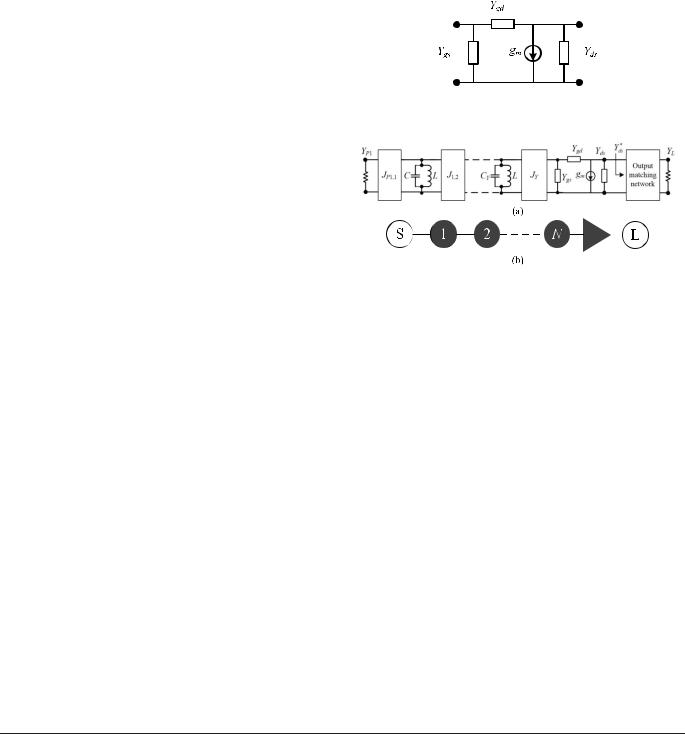
A transistor is, in practice, a bilateral device, where the output load influences the input port impedance. Before deriving the active N + 3 coupling matrix below, a simplified admittance network used to represent the transistor in small-signal operation is introduced in Fig. 1 [25].
The Y matrix describing the transistor is given by [25]
[ |
|
] = |
gm |
+ Ygd |
Yds |
|
Ygd |
|
|
YT |
|
Ygs |
Ygd |
−Ygd |
(1) |
||
|
|
|
|
− |
|
+ |
|
|
where Ygs , Ygd , and Yds are the admittances between the source, drain, and gate; gm is the voltage-controlled current source representing the transconductance.
Fig. 2(a) shows a circuit of an Nth-order filter using lumped element representations of the resonators based on
Fig. 1. Equivalent lumped circuit of a small-signal model for a transistor.
Fig. 2. Topology and equivalent lumped circuit for a coupled resonators filter-amplifier circuit. (a) Lumped circuit model. (b) Schematic of the circuit.
parallel capacitors and inductors coupled by J inverters. The load of the filter, in this case, is the transistor. The circuit shown in Fig. 2(a) is represented schematically in Fig. 2(b), where the resonators are represented by black filled circles and the clear circles denote the source and the load.
The input port admittance of the filter is denoted by YP1. The Nth resonator is directly coupled to the transistor by the inverter JY . A matching network is employed at the output to transfer the load YL to Yds , conjugately matched to the drain- to-source admittance Yds . The load admittance YL represents the measurement port at the output, which is usually 50 .
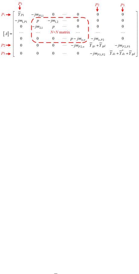
We recall that the aim of formulating this topology is to demonstrate a filter response with gain, and for our demonstrator, a Chebyshev response will be synthesized. Kirchoff’s laws can be applied to the circuit in Fig. 2(a) to write down the equations at each circuit nodes. The resulting Y matrix is given in (2), shown at the bottom of this page. Following the matrix scaling process described in [26] and [27], this N + 3 matrix [Y ] in (2) can now be manipulated to derive matrix [A] shown in Fig. 3. This N + 3 matrix has the rows and columns P1, P2, and P3 for the filter’s input, the transistor’s input, and the load with matching, surrounding the conventional N × N general coupling matrix. The diagonal entries, AP1, P1, AP2, P2, and AP3, P3 indicate the input admittance of the filter,
|
|
|
|
YP1 |
|
1− j JP1,1 |
|
|
0 |
|
· · · |
|
|
|
|
0 |
|
|
|
|
|
0 |
|
|
|
|
0 |
|
|
|
|
|
|||
|
|
|
|
− j J1, P1 |
|
|
+ j ωC |
|
− j J1,2 |
· · · |
|
|
|
|
0 |
|
|
|
|
|
0 |
|
|
|
|
0 |
|
|
|
|
|
||||
|
|
|
j ω L |
|
|
|
|
|
|
|
|
|
|
|
|
|
|
|
|
|
|||||||||||||||
|
|
|
|
|
|
|
|
1 |
|
|
|
|
|
|
|
|
|
|
|
|
|
|
|
|
|
|
|
|
|
|
|
|
|
|
|
|
|
|
|
0 |
|
|
j J2,1 |
|
|
|
j ωC |
|
|
|
|
|
|
0 |
|
|
|
|
|
0 |
|
|
|
|
0 |
|
|
|
|
|
|
|
|
|
|
|
j ω L |
|
|
|
|
|
|
|
|
|
|
|
|
|
|
|
|
|
|
|
|||||||||||
|
|
|
|
|
|
− |
|
+ |
|
|
|
|
|
|
|
|
|
|
|
|
|
|
|
|
|
|
|
|
|
|
|
|
|||
|
|
|
|
|
|
|
|
|
|
· · · |
|
|
|
|
|
|
|
|
|
|
|
|
|
|
|
|
|
|
|
|
|
|
|||
[ |
Y |
] = |
. |
|
|
. |
|
|
. |
|
. |
. . |
|
|
|
|
. |
|
|
|
|
|
. |
|
|
|
|
. |
|
|
|
|
|
(2) |
|
|
.. |
|
|
.. |
|
|
.. |
|
|
|
|
|
|
.. |
|
|
|
|
|
.. |
|
|
|
|
.. |
|
|
|
|
|
|
||||
|
|
|
|
|
|
|
|
|
|
|
|
|
|
|
|
|
|
|
|
|
|
|
|
|
|
|
|
|
|
|
|
|
|
|
|
|
|
|
|
|
|
|
|
|
|
|
|
|
|
1 |
|
|
|
|
|
|
|
|
|
|
|
|
|
|
|
|
|
|
|
|
|
|
|
|
|
0 |
|
|
0 |
|
|
0 |
|
|
|
|
|
|
|
|
j ωC |
|
|
|
|
j J |
|
|
|
0 |
|
|
|
|
|
||
|
|
|
|
|
|
|
|
|
|
j ω L |
|
Y |
|
|
|
|
|
|
|
|
|
|
|||||||||||||
|
|
|
|
|
|
|
|
|
|
|
|
· · · |
|
|
|
− |
|
Y |
|
|
|
|
|
|
|
|
|
|
|||||||
|
|
|
|
|
|
|
|
|
|
|
|
|
|
+ |
|
|
|
|
|
|
|
|
|
|
|
|
|
|
|
|
|||||
|
|
|
|
0 |
|
|
0 |
|
|
0 |
|
|
|
|
|
|
|
j J |
|
|
Y |
gs |
+ |
Y |
gd |
− |
Y |
gd |
|
|
|
|
|||
|
|
|
|
|
|
|
|
|
|
|
|
· · · |
|
|
− |
|
Y |
|
|
|
|
|
|
|
|
|
|||||||||
|
|
|
|
0 |
|
|
0 |
|
|
0 |
|
|
|
0 |
|
|
|
g |
m − |
Y |
gd |
Y |
Y |
|
+ |
Y |
gd |
|
|
||||||
|
|
|
|
|
|
|
|
|
|
|
|
· · · |
|
|
|
|
|
|
|
|
|
|
ds + |
|
ds |
|
|
|
|||||||
This article has been accepted for inclusion in a future issue of this journal. Content is final as presented, with the exception of pagination.
GAO et al.: COUPLING MATRIX-BASED DESIGN OF WAVEGUIDE FILTER AMPLIFIERS |
3 |
Fig. 3. Matrix [ A] showing the general N × N coupling matrix surrounded by extra columns and rows.
the input admittance of the transistor, and the transistor’s load admittance with a matching network included.
Matrix [A], shown in Fig. 3, can be further decomposed into three matrices [28]
[ A] = [T ] + p · [U ] − j · [m] |
(3) |
where the [T ] matrix, expanded later in (14), includes the filter’s port admittance, the input admittance of the transistor, and the load admittance. In (3), [U ] is the identity matrix except for entries UP1, P1, UP2, P2, and UP3, P3, which are zero. p is the complex frequency variable defined in [28] as
1 |
|
ω |
− |
ω0 |
. |
|
|
p = j |
|
|
|
(4) |
|||
FBW |
ω0 |
ω |
|||||
Here, FBW is the fractional bandwidth and ω0 is the center frequency. The matrix [m] in (3) is the coupling matrix, of which mi, j denotes the interresonator coupling and m Pk,i = mi, Pk are the coupling between ports and resonators (i = 1 to N; k = 1–3). The terms m P2, P3 and m P3, P2 are the couplings between the transistor’s input and load. For the matrix [A],
shown in Fig. 3, as the common |
factor − j is extracted |
||||||||||||
as − j [m], the |
normalized |
coupling coefficients in |
the |
||||||||||
transistor become |
|
|
|
|
|
|
|
|
|
|
|
|
|
|
|
|
|
|
|
|
|
|
gd − |
|
m |
. |
|
|
|
|
Y |
|
Y |
|
|||||||
m |
P2, P3 |
= |
gd |
m |
P3, P2 = |
|
g |
(5) |
|||||
|
|
|
|
|
|
||||||||
|
|
j |
|
|
j |
|
|||||||
Compared with the general coupling matrix, three more entries of the [m] matrix are modified to achieve a Chebyshev input matching, namely the selfcoupling mn,n , and the external couplings from the Nth resonator to the transistor,
mn, P2 and m P2,n. The value of mn,n , m P2,n, and mn, P2 |
are |
|||||||||
given by |
|
|
|
|
|
|
|
|
|
|
mn,n |
= − |
|
b |
|
|
|
|
|
(6) |
|
|
|
|
|
|
||||||
a · gn gn+1 |
||||||||||
mn, P2 |
= |
m P2,n |
|
|
|
a2 + b2 |
|
|
(7) |
|
|
a · gn gn+1 |
|||||||||
|
|
|
= |
|
|
|||||
where gn and gn+1 are the standard g values that are defined and calculated in [28]. a and b are the normalized real and imaginary parts of the transistor’s input admittance Y in and
can be calculated from the transistor’s Y matrix parameters
|
|
|
Re |
|
gd [ |
|
m + |
|
|
ds + |
|
|
ds ] |
|
|
gs |
|
|||||
|
|
|
Y |
Y |
Y |
|
|
|||||||||||||||
|
a |
= |
g |
+ |
(8) |
|||||||||||||||||
Y |
||||||||||||||||||||||
|
|
|
|
|
|
|
|
|
|
|
|
|
|
|||||||||
|
|
Y gd + Y ds + Y ds |
||||||||||||||||||||
|
|
|
|
|
|
|
|
|||||||||||||||
|
|
|
Im |
|
gd [ |
|
m + |
|
ds + |
|
ds ] |
|
|
gs |
|
|||||||
|
|
|
Y |
Y |
Y |
|
|
|||||||||||||||
|
b |
= |
g |
+ |
(9) |
|||||||||||||||||
Y |
||||||||||||||||||||||
|
|
|
|
|
|
|
|
|
|
|
|
|
|
|||||||||
|
|
Y gd + Y ds + Y ds |
||||||||||||||||||||
|
|
|
|
|
|
|
|
|||||||||||||||
Y |
in = a + j b. |
|
|
|
(10) |
|||||||||||||||||
Note that the term jmn,n visible at the bottom right corner of the N × N matrix shown within the red dotted line in Fig. 3 represents a frequency shift of the last resonator in the filter. This has been observed before for the case of transistors, mixers, and antennas, and is described in [29]. The shift in frequency is described by mn,n in (6), allowing the Chebyshev (or other) filtering response to be maintained independently of the nature of the complex input impedance of the transistor. This frequency shift can be positive or negative depending upon the imaginary part of the input admittance.
The following relationships can be used to calculate the S-parameters for the complete circuit [26], [28], [30]:
S11 |
= 2[ A]−P11, P1 − 1 |
(11) |
||||
S21 |
= 2 |
Re( |
|
ds ) |
[ A]−P31, P1. |
(12) |
Y |
||||||
III. FILTER-AMPLIFIER DESIGN USING
COUPLING MATRIX APPROACH
In this section, the design procedure and simulation results for an X-band rectangular waveguide filter-amplifier are described. Before discussing the design procedure, it is informative to illustrate the completed filter-amplifier component, which is shown in Fig. 4.
Port 1 is assigned to the waveguide port, and Port 2 refers to the 50microstrip output port. As shown in Fig. 4, the two-pole waveguide filter is comprised of Resonator 1 and Resonator 2, which are waveguide TE101 cavities coupled via asymmetrical capacitive irises. Resonator 2 is formed by a waveguide cavity and the transistor coupling probe, interconnecting transmission line and the transistor. A reduced height section of the waveguide forms a platform on which the microstrip substrate is located. The substrate has the probe and

This article has been accepted for inclusion in a future issue of this journal. Content is final as presented, with the exception of pagination.
4 |
IEEE TRANSACTIONS ON MICROWAVE THEORY AND TECHNIQUES |
TABLE I
VALUES OF THE TRANSISTOR’S Y MATRIX PARAMETERS
Fig. 4. Layout of the waveguide filter-amplifier. (a) 3-D view of the internal waveguide and the microstrip circuit. (b) Sectional view of the filter and platform for the transistor circuit.
transmission line, and also the transistor with bias connections placed on it.
A. Circuit Response Calculation Using the Coupling Matrix
The values of the coupling coefficients are given by the standard expressions for the desired filter response except for the couplings mn,n , m P2,n, and mn, P2. The filter and transistor specifications can be translated into elements of the N + 3 coupling matrix in Fig. 3 using standard tables or formulas [27], [28]. Here, we will use an example of a two-pole Chebyshev filter with a center frequency f0 of 10 GHz, a bandwidth of 500 MHz [fractional bandwidth (FBW) = 0.05], and a passband return loss of 20 dB. The transistor used is an NE310S01 with unnormalized parameters Y and normalized parameters Y (i.e., scaled by Y0 = 0.02 S) summarized in Table I [25], [31]. It should be noted that the Y matrix parameters employed here are calculated assuming that the transistor operates at 10-GHz center frequency, and the operating conditions of the transistor are drain-to-source voltage Vds = 2 V and drain current Ids = 10 mA.
Based on the prototype Chebyshev low-pass filter and the normalized transistor’s Y matrix parameters, the active coupling matrix [m] can be calculated according to (6), (8), and (9) to give (13), shown at the bottom of this page.
This coupling matrix is asymmetric because of the active element. The matrix [T ], used to describe the filter ports admittance and the transistor’s input and output, is given by
|
|
0 |
0 |
0 |
|
0 |
|
|
0 |
|
|
|
|
1 |
0 |
0 |
|
0 |
|
|
0 |
|
|
[ |
T |
0 |
0 |
0 |
0.2692 |
0 |
1.5428 j |
|
0 |
|
. |
|
] = 0 |
0 |
0 |
+ |
|
0 |
|
|
|||
|
|
|
0 |
0 |
|
|
0.5668 |
|
0.1630 j |
|
|
|
|
0 |
|
0 |
|
+ |
|
||||
|
|
|
|
|
|
|
|
|
|
|
|
|
|
|
|
|
|
|
|
|
|
(14) |
|
Using (11) and (12), the resultant scattering parameters can be calculated from the active coupling matrix and are presented in Fig. 5(a). The novel active coupling matrix produces a standard Chebyshev response with amplification.
As well as the coupling matrix response, Fig. 5(b) shows the response from an ADS circuit simulation [in Fig. 5(c)] using the full frequency variation of the input impedance of the transistor and the constant Yin. As can be seen, the agreement is good, showing in the case that approximating Yin as a constant has a little effect.
B. Physical Design of the Waveguide Filter-Amplifier
The coupling matrix in Section III-A was based on normalized admittance parameters, and assumed that the normalized admittance stayed consistent from the input to output; this works well and results in good prediction of the circuit response as shown in Fig. 5(a). Matrix [ A] scaled from admittance matrix [Y ] enables us to ignore the matching and admittance conditions and to concern ourselves with just the coupling coefficients in the coupling matrix [m]. That is, the fact that the coupling matrix of Fig. 3 is derived assuming a consistent normalized admittance does not matter, and it can be used with, for example, the waveguide and the microstrip without reference to their admittance. This is exactly the same
|
|
1.2264 |
1 |
. 0 |
1.6621 |
|
0 |
|
0 |
|
|
|
||
|
|
|
0 |
2264 |
0 |
|
0 |
|
0 |
|
|
|
||
[ |
m |
|
0 |
1.6621 |
−1.0762 |
2.3407 |
0.1629 |
0 |
0.0164 j |
|
(13) |
|||
|
] = |
0 |
|
0 |
2.3407 |
|
0 |
− |
|
|
||||
|
|
|
0 |
|
0 |
0 |
6.9129 |
|
3.46578 j |
|
|
|
|
|
|
|
|
|
+ |
|
0 |
|
|
|
|||||
|
|
|
|
|
|
|
|
|
|
|
|
|
|
|

This article has been accepted for inclusion in a future issue of this journal. Content is final as presented, with the exception of pagination.
GAO et al.: COUPLING MATRIX-BASED DESIGN OF WAVEGUIDE FILTER AMPLIFIERS |
5 |
Fig. 5. (a) Calculated filter-amplifier response using the coupling matrix formulation. (b) Comparison of the S-parameters response of circuit simulation using constant Yin and the full frequency variation of the input impedance of the transistor. (c) Circuit schematic in ADS.
Fig. 6. Coupled waveguide cavities and the process to extract the coupling coefficients. (a) Structure to determine the physical dimension of the coupling aperture. (b) Coupling coefficients versus dimension d1. All points are at 10 GHz.
as in conventional filter design using the coupling matrix and is one of its great strengths.
Hence, in practice, the geometries of the coupling gaps in the input waveguide filter and the physical structure of the transition from the waveguide to the microstrip input of the transistor can be determined from the coupling matrix [m] in (13). The process and equations follow closely from just a simple filter [28], and this is discussed in the Appendix. The design process is discussed below.
The first step is to determine the interresonator coupling strength. As with just a conventional simple filter, the coupling coefficient m1,2 = m2,1 between the two resonators is scaled
by the FBW from the coupling matrix [m] in (13) |
|
M1,2 = FBW · m1,2 M2,1 = FBW · m2,1. |
(15) |
For this example, M1,2 = 0.0831. The coupling coefficients can be realized by a suitable gap in the wall between waveguide resonators. A pair of waveguide-coupled resonators, shown in Fig. 6(a), are simulated in a full-wave simulator; CST was used here. This is in order to find the target coupling coefficient M1,2 [28]. There is weak coupling to the input and output via a narrow capacitive gap, as shown in Fig. 6(a). The coupling coefficient M1,2 between the two resonators can be altered by varying the iris gap d1. A graph
Fig. 7. Waveguide structure to extract the quality factor for Resonator 1.
(a) Structure to determine physical dimension for waveguide cavity with the quality factor. (b) External quality factors Qe versus dimension d2. All points are at 10 GHz.
of the coupling coefficient M1,2, as shown in Fig. 6(b), can be plotted [28]. The coupling coefficient given in (15) can now be located and is shown in Fig. 6(b), and hence, a d1 of 2.85 mm can be found.
The next step is to determine the iris size at port 1 of the waveguide filter. This can be done by extracting the external quality factor of Resonator 1 (Qe1). In the N + 3 coupling
matrix, Qe1 is related to the external couplings |
|
|||||
Qe1 = |
1 |
= |
1 |
, m P1,1 |
= m1, P1 |
. (16) |
|
|
|||||
FBW·m12, P1 |
FBW·m2P1,1 |
|||||
From (13) and (16), it is found that the external quality factor required is Qe1 = 13.297. Fig. 7 shows the setup for determining Qe1, i.e., the quality factor at the input to the waveguide filter. The S-parameter response, generated by simulating the single-waveguide resonator in Fig. 7(a), is a single resonance curve, and Qe1 is extracted by calculating its quality factor. Changing the iris length d2 alters the values of Qe1, and this is shown in Fig. 7(b). As shown in the graph, for example, we can find a value of d2 = 4.85 mm for the input iris to the filter. Note that both the interresonator coupling [see Fig. 6(b)] and the external quality factor [see Fig. 7(b)] are evaluated at 10 GHz, the center frequency of the filteramplifier.
Now, we need to consider the connection to the transistor via Resonator 2, as shown in Fig. 4. This comprises a combination of the waveguide cavity and planar circuit elements including the transistor itself. This is depicted in Fig. 8(a). Through an E-field probe, Resonator 2 is directly coupled to the transistor’s input, which is a complex value impedance.
The coupling strength from the resonator to the transistor is related to m = m2, P2 = 2.3407, and the selfcoupling m2,2 = −1.0762 related to the center frequency of Resonator 2, and all these couplings can be achieved by constructing appropriate geometries of the structure shown in Fig. 8(a). The external coupling m = m2, P2 mainly depends on the coupling structure, that is, the probe length (l) and the interconnecting transition length (s). The selfcoupling m2,2 mainly depends upon the length of Resonator 2 (L2).
The next step is to determine the values of l, s, and L2 that fulfill the required external couplings and selfcoupling in (13). However, the physical dimensions corresponding

This article has been accepted for inclusion in a future issue of this journal. Content is final as presented, with the exception of pagination.
6 |
IEEE TRANSACTIONS ON MICROWAVE THEORY AND TECHNIQUES |
Fig. 9. Layout of the microstrip transistor part. Length t2 is a single-stub matching for the output of the transistor to the 50transmission line.
Fig. 8. Setup to extract the external quality factor for Resonator 2 incorporating the transistor’s input. (a) Structure for extracting the eternal quality factor of Resonator 2 interconnecting the input of the transistor. (b) QeT extraction setup in CST. (c) External quality factor Qe versus interconnection length s. All points are at 10 GHz.
m = m2, P2 cannot be extracted directly as for the waveguide case in Fig. 7. Instead, the m P2,2 = m2, P2 and m2,2 can be evaluated by the S-parameter response of the combined structure of Resonator 2 incorporating the probe and input of the transistor.
In the practical design, the external coupling m P2,2 = m2, P2 and selfcoupling m2,2 can be determined by extracting the external quality factor (QeT ) and the resonant frequency ( fT ) of Resonator 2 incorporating the input of the transistor. The derivations of the frequency ( fT ) and quality factor (QeT ) are given in the Appendix, and fT and QeT can be calculated using the external coupling m P2,n = mn, P2 and selfcoupling mn,n. Significantly, the Appendix also shows that fT = f0 and QeT = Qe1, and this fact now allows the design procedure to continue in exactly the same way as for a conventional filter, that is, the same as for the above-described input port.
The whole structure includes the resonator itself and the complex input impedance of the transistor, as well as the transition from the waveguide to the microstrip. This mixed resonator-microstrip construction can be simulated in CST, and the appropriate dimensions are found to fulfill the requirement of, in this case, QeT = 13.297 at the center frequency fT = 10 GHz.
The simulation of the single resonator, as shown in Fig. 8(b), was performed in CST, and a resonance frequency and the external quality factor are determined. As the setup schematically depicts in Fig. 8(b), the microstrip port is connected to port 2 in CST, with Port 2 load set to be the input impedance of the transistor. Port 1 is set to be the value of waveguide impedance; then, the whole structure is simulated. The microstrip circuit in Fig. 8(a) is modeled using the RT/5870 substrate with a thickness of 0.254 mm and a relative dielectric constant εr = 2.33. The center frequency is mainly determined by the length of the resonator (L2), the length of
Fig. 10. Circuit design for the transistor amplifier. (a) Equivalent lumped circuit of the matching filter. (b) Constant-gain and constant-noise figure circles.
the E-field probe (l), and the length of the feed transmission line (s). In the simulation, the width of the feed line and probe (w1, w3) are kept constant, and only the dimensions of l and s are changed. During this tuning process, L2 is adjusted to keep the center frequency at 10 GHz. The simulation results are shown in Fig. 8(c) from which the appropriate lengths of L2, l, and s can be chosen to achieve the target QeT = 13.297.
To complete the discussion, here, we briefly introduce the microstrip transistor circuit design. The microstrip part of the device consists of the probe, feed transmission line, transistor, bias circuits, and output matching stub. The output matching network is assumed to conjugately match to Yds as shown in Fig. 2(a). The characteristic impedance of the output transmission line of width w2 is 50 . The lengths of t1 and t2 are found using the single-stub matching method in [25]. The lengths b1 + b2 and b3 + b4 are quarter-wavelength long bias tees at 10-GHz center frequency and are connected to the via-ground holes through 100-pF surface mount capacitors. Square pads are located at the end of the bias tees to connect the dc power. The ground of the PCB is connected to the base of the platform by pressure. The simulated operating conditions of the transistor are drain-to-source voltage Vds = 2 V and drain current Ids = 10 mA [31]. The layout of the microstrip circuit is shown in Fig. 9.
The simulated noise performance for the matched amplifier is shown in Fig. 10. In the Smith chart [see Fig. 10(b)], the impedance synthesized at the transistor input port is superimposed over the device noise and gain contours. The reflection

This article has been accepted for inclusion in a future issue of this journal. Content is final as presented, with the exception of pagination.
GAO et al.: COUPLING MATRIX-BASED DESIGN OF WAVEGUIDE FILTER AMPLIFIERS |
7 |
TABLE II
VALUES OF INITIAL AND NORMALIZED FILTER-AMPLIFIER PARAMETERS
coefficient looking into the source S [see Fig. 10(a)] has been calculated [28] and is shown on the Smith chart [see Fig. 10(b)], where 14.3-dB gain circle and 0.78-dB noise figure circle intersect. Recalling the aim of our work is to demonstrate the filter-amplifier with the Chebyshev response using the N + 3 coupling matrix, and this noise figure has not been further optimized.
All the parameters necessary to form the filter-amplifier have been determined as discussed above. Therefore, the complete component can be simulated. The microstrip part, including the transistor model, is simulated in ADS to generate an S2P. Then, this cosimulation is combined in CST with the waveguide model and microstrip part for the complete filteramplifier structure. The parameters used for the simulations are given in Table II and are the same as the values shown in the design graphs in Figs. 6(b), 7(b), and 8(c). Table II shows the initial values and optimized values. Optimization goals, in this case, are set to be: from 9.75 to 10.25 GHz, S11 is under −20 dB; from 9.75 to 10.25 GHz, S22 is under −10 dB; and critical points 9.824 and 10.178 GHz are under −40 dB.
Both the initial response and an optimized response, using the sizes specified in Table II, are shown in Fig. 11. The optimized results in Fig. 11(a) and (b) show that over the passband, S11 is below −20 dB, S21 shows gain around 13 dB, and S22 is below −10 dB. The good correlation between the initial and optimized responses demonstrates the validity of the coupling matrix technique in providing starting values for the waveguide filter-amplifier design process. Fig. 11(c) shows a noise figure (NF), which is about 1.10 dB over the passband, and the minimum NF for the device is 1.02 dB at 9.85 GHz. The real and imaginary parts of the input impedance of the transistor are shown in Fig. 11(d).
IV. FABRICATION AND MEASUREMENTS
The waveguide structure is made in two halves cut along the E-plane and is machined from aluminum (AL5083) on a CNC machine. The microstrip circuit is fabricated on the 0.254-mm thickness RT/5870 substrate. Fig. 12 shows a photograph of the device.
The measurement is performed using an Agilent PNA E8362B vector network analyzer referenced to the input
Fig. 11. Cosimulation results of the waveguide filter integrated with the amplifier. (a) Scattering parameters S11 and S21. (b) Scattering parameters S22 and S12. (c) Noise figure. (d) Input impedance of the transistor.
Fig. 12. Photograph for the fabricated device.
and output ports. As the picture in Fig. 13(a) shows, the input waveguide flange is connected to port 1 using a WR-90 coaxial-to-waveguide adapter with losses <0.1 dB. The setup is calibrated with coaxial standards without the adaptor. Thus, the measurements do include the tiny effect of the coaxial cable-to-waveguide adapter. The 50microstrip output is connected to port 2 of the analyzer through an SMA connector. Bias condition of the transistor is provided by a gate-to-source voltage of Vgs = −0.52 V and drain-to-source voltage of Vds = 2.2 V. The measured S-parameters response is compared with the simulated one in Fig. 13(b) and (c) and displays a good agreement with the two-pole Chebyshev filtering characteristic and also a gain. The measured in-band small-signal gain is within 11.7 ± 0.46 dB from 9.75 to 10.25 GHz. The measured input and output return losses are around 13.8 and 10.62 dB, respectively, over the passband. The disagreement may be caused by the fabrication tolerances and any deviation of the transistor parameters from its data sheet. The 1-dB compression point examined at 10 GHz is about −2.9 dBm as shown in Fig. 13(d).

This article has been accepted for inclusion in a future issue of this journal. Content is final as presented, with the exception of pagination.
8 |
IEEE TRANSACTIONS ON MICROWAVE THEORY AND TECHNIQUES |
Fig. 13. Circuit simulation and measurement results. (a) Measurement setup.
(b) Scattering parameters S11 and S21. (c) Scattering parameters S22 and S12.
(d) P1 dB measurement.
V. CONCLUSION
This paper described a novel active coupling matrix with transistor parameters included; it is used to synthesize a specified filter response including gain. The extended N + 3 active coupling matrix builds on the general N + 2 coupling matrix formulation. The resulting N + 3 active coupling matrix can be used to generate the necessary matrix elements from which circuit optimization is performed. This allows the prediction of the response for the filter-amplifier and provides the initial values of the waveguide filter structure. Semiempirical simulation trials can be used to realize the physical geometries corresponding to the matrix values for a given circuit technology. Further applications of matching a complex port through the resonator circuit can be generalized to other components, e.g., mixers, antennas, and so on.
The topology proposed here makes it possible to extend this methodology to amplifier circuits resonator matched both at the input and output ports. Although in this example only input resonators matching circuits are employed, this approach is currently being extended for matrix descriptions, which incorporate both input, interstage, and output resonators matching, for multistage amplifiers.
For conventional filters, although the coupling matrix is essentially a narrowband approach, good use is made of the technique even when the filter bandwidths become larger. The matrix only needs to give a good estimate for the physical dimensions, so the final optimization is possible. Of course, this filter-amplifier co-design approach can be generalized to wideband amplifiers design by introducing a frequency-variant model of the transistor, but this is not possible with the current coupling matrix.
For this demonstrator, a microstrip circuit containing the transistor is combined with a WR-90 rectangular waveguide. Combining the filter design with the active element can allow for more compact components. Elements of the matching network have been transferred to waveguide resonators,
Fig. 14. Equivalent lumped circuit the Nth resonator coupled to the input admittance of the transistor.
shrinking the overall size of the device and also increasing the port-to-port isolation. It is also noted that waveguide high-Q filter structures can be employed to offer lower loss impedance matching/filtering functions to the active devices. This latter effect will become more significant as the operating frequency, and therefore, planar circuit losses increase.
APPENDIX
Here, we calculate the center frequency fT and the external quality factor QeT of the last resonator in the filter when it is connected to the transistor input.
The equivalent lumped circuit of the Nth resonator coupled to the input admittance of the transistor (Yin) is shown in Fig. 14. The input admittance of the transistor Yin, which is a complex value, is coupled through the inverter JY . Referring [26] and [27], the capacitor CY and the inverter JY can be expressed in terms of selfcoupling mn,n and external couplings
m P2,n = mn, P2 by
CY = C(1 − FBW · mn,n ) |
(17) |
JY = FBWω0C · Y0 · mn, P2 = FBWω0C · Y0 · m P2,n
(18)
where C is the capacitance of the first to the (N − 1)th resonators in Fig. 2. The value of transistor’s admittance Yin is given by
Yin = (a + j b) · Y0. |
(19) |
The input admittance of the circuit in Fig. 14 can now be calculated and compared with the standard equation for the admittance of a loaded resonant circuit. The input admittance (Yres) of the Nth resonator incorporating Yin can be expressed as
|
|
|
|
|
|
|
1 |
|
|
J |
2 |
|
|
|
|
|
|
||
|
Yres = j ωCY + |
|
|
|
+ |
Y |
|
. |
|
|
|
|
(20) |
||||||
|
j ω L |
Yin |
|
|
|
|
|||||||||||||
Substitute (17)–(19) into (20), we have |
ω02 |
· m P2,n |
|||||||||||||||||
Yres |
j ωC 1 |
FBW mn,n |
|
|
|
b · |
|
2 |
|
||||||||||
= |
− |
· |
|
|
− |
|
|
FBW |
|
|
|
|
|
2 |
|
|
|||
|
|
|
|
(a |
+ |
b ) |
· |
ω |
|
||||||||||
|
|
|
|
|
|
|
|
|
|
|
|
|
|
|
|
||||
|
|
+ |
1 |
|
+ |
a · FBWω0C · m2P2,n |
. (21) |
||||||||||||
|
|
j ω L |
|
|
|
|
(a2 + b2) |
||||||||||||
At the center frequency (ωT ), where for the narrowband approximation (ω = ωT ), Yres satisfies
Im(Yres)|ω=ωT = 0. |
(22) |

This article has been accepted for inclusion in a future issue of this journal. Content is final as presented, with the exception of pagination.
GAO et al.: COUPLING MATRIX-BASED DESIGN OF WAVEGUIDE FILTER AMPLIFIERS |
9 |
Substitute (21) into (22), yielding
|
|
ω0 |
|
2 |
|
|
b |
FBW m2P2 |
, |
n |
|
|
ω0 |
|
|
|
|
|
|
|
|
|
|||||||
|
|
|
|
|
|
+ |
|
· |
· |
|
|
|
|
|
|
− (1 |
− FBW · mn,n ) = 0. |
||||||||||||
ω |
T |
|
|
(a2 |
b2) |
|
|
|
ω |
T |
|||||||||||||||||||
|
|
|
|
|
|
|
|
|
|
+ |
|
|
|
|
|
|
|
|
|
|
|
|
|
(23) |
|||||
|
|
|
|
|
|
|
|
|
|
|
|
|
|
|
|
|
|
|
|
|
|
|
|
|
|
|
|||
Then, (23) can be solved to give |
|
|
|
|
|
|
|
|
|
||||||||||||||||||||
|
|
|
|
|
|
|
|
|
b· |
2 |
· |
2P2,n |
|
|
|
|
|
|
|
|
|
|
|
|
|
||||
|
|
|
|
|
|
|
|
|
|
· |
|
2 |
· |
2P2,n |
|
2 |
4(1 |
FBW mn,n ) |
|||||||||||
|
ω0 |
|
|
|
− |
|
(a b ) ± |
|
|
|
(a b ) |
|
|
+ − |
· |
|
|
|
|||||||||||
|
|
|
|
|
|
|
|
|
|
FBW m2 |
|
|
|
b FBW m2 |
|
|
|
|
|
|
|
||||||||
|
|
|
|
= |
|
|
|
|
+ |
|
|
|
|
|
|
|
|
+ |
|
|
|
|
|
|
. |
||||
ωT |
|
|
|
|
|
|
|
|
|
|
|
|
|
|
|
2 |
|
|
|
|
|
||||||||
|
|
|
|
|
|
|
|
|
|
|
|
|
|
|
|
|
|
|
|
|
|
|
|
|
|
|
(24) |
||
Because the ratio of ωT |
and ω0 |
should be positive, only the |
|||||||||||||||||||||||||||
positive root is used. Substituting ωT = 2π fT |
and ω0 = 2π f0 |
||||||||||||||
into (24), the center frequency |
fT can be calculated as |
|
|
||||||||||||
fT = |
|
|
|
|
|
2(a2 + b2) · f0 |
|
|
|
|
|
. |
|||
|
|
|
|
|
|
|
|
|
|
|
|
||||
|
· |
|
· |
n, P2 |
|
+ |
|
2 |
|
2 2 |
− |
||||
|
|
|
|
b2·mn4,P2·FBW2 |
|
|
|||||||||
|
b |
|
FBW |
|
m2 |
1 |
|
4(1−mn,n ·FBW)(a |
+b ) |
|
1 |
|
|||
|
|
|
|
|
|
|
|
|
|
|
|
|
|
(25) |
|
As the admittance Yres is given in (21), the external quality factor QeT can be calculated by [28]
|
|
fT |
|
2 |
|
2 |
2 |
|
|
|
b |
|
QeT |
= |
(a2 + b ) |
− |
mn,n · (a |
+ b |
) |
|
. (26) |
||||
|
f0 |
|
a·FBWm P2,n |
a · m P2,n |
|
|
− a |
|||||
It is interesting to substitute m P2,2 = m2, P2 |
= 2.3407 and |
|||||||||||
m2,2 = −1.0762 in the coupling matrix (13) into (25) and (26); the external Q of Resonator 2 coupled with Yin can be calculated to give QeT = 13.297, and the resonant frequency is calculated as fT = 10 GHz.
Now, recalling m P2,n = mn, P2 and mn,n , which are defined in (6) and (7), the final step is to substitute (6) and (7) into
(25) and (26), respectively, to give the simple solutions |
|
||
fT = f0 |
|
(27) |
|
QeT = |
gn gn+1 |
= Qe1. |
(28) |
FBW |
|||
It can be seen from (27) and (28) that the external Q and center frequency of the resonator coupled with the active component are the same as the case for conventional filters [28]. That is, QeT = Qe1 even though the load is complex. This fact allows the method of designing the filter-amplifiers to much more closely resemble the design of a standard filter [28].
ACKNOWLEDGMENT
The authors would like to thank P. Gardner and T. Jackson with the University of Birmingham for their assistance with the measurement and W. Hay for fabricating the waveguide.
REFERENCES
[1]W. Deal, X. B. Mei, K. M. K. H. Leong, V. Radisic, S. Sarkozy, and R. Lai, “THz monolithic integrated circuits using InP high electron mobility transistors,” IEEE Trans. THz Sci. Technol., vol. 1, no. 1, pp. 25–32, Sep. 2011.
[2]M. Abdolhamidi and M. Shahabadi, “X-band substrate integrated waveguide amplifier,” IEEE Microw. Wireless Compon. Lett., vol. 18, no. 12, pp. 815–817, Dec. 2008.
[3]B. Ahmadi and A. Banai, “Substrateless amplifier module realized by ridge gap waveguide technology for millimeter-wave applications,”
IEEE Trans. Microw. Theory Techn., vol. 64, no. 11, pp. 3623–3630, Nov. 2016.
[4]H. Yang et al., “WR-3 waveguide bandpass filters fabricated using high precision CNC machining and SU-8 photoresist technology,” IEEE Trans. THz Sci. Technol., vol. 8, no. 1, pp. 100–107, Jan. 2018.
[5]X. Shang et al., “W -Band waveguide filters fabricated by laser micromachining and 3-D printing,” IEEE Trans. Microw. Theory Techn., vol. 64, no. 8, pp. 2572–2580, Aug. 2016.
[6] J.-Q. Ding, S.-C. Shi, K. Zhou, D. Liu, and W. Wu, “Analysis of 220-GHz low-loss quasi-elliptic waveguide bandpass filter,” IEEE Microw. Wireless Compon. Lett., vol. 27, no. 7, pp. 648–650, Jul. 2017.
[7]K. M. K. H. Leong et al., “WR1.5 silicon micromachined waveguide components and active circuit integration methodology,” IEEE Trans. Microw. Theory Techn., vol. 60, no. 4, pp. 998–1005, Apr. 2012.
[8]B. Thomas et al., “A broadband 835–900-GHz fundamental balanced mixer based on monolithic GaAs membrane Schottky diodes,” IEEE Trans. Microw. Theory Techn., vol. 58, no. 7, pp. 1917–1924, Jul. 2010.
[9]A. U. Zaman, V. Vassilev, P.-S. Kildal, and H. Zirath, “Millimeter wave E-plane transition from waveguide to microstrip line with large substrate size related to MMIC integration,” IEEE Microw. Wireless Compon. Lett., vol. 26, no. 7, pp. 481–483, Jul. 2016.
[10]A. Aljarosha, A. U. Zaman, and R. Maaskant, “A wideband contactless and bondwire-free MMIC to waveguide transition,” IEEE Microw. Wireless Compon. Lett., vol. 27, no. 5, pp. 437–439, May 2017.
[11]Z. Y. Malik, A. Mueed, and M. I. Nawaz, “Narrow band ridge waveguide-to-microstrip transition for low noise amplifier at Ku-band,” in Proc. 6th Int. Bhurban Conf. Appl. Sci. Technol., Islamabad, Pakistan, Jan. 2009, pp. 140–143.
[12]P. G. Courtney, J. Zeng, T. Tran, H. Trinh, and S. Behan, “120 W Ka band power amplifier utilizing GaN MMICs and coaxial waveguide spatial power combining,” in Proc. IEEE Compound Semiconductor Integr. Circuit Symp. (CSICS), Oct. 2015, pp. 1–4.
[13]T. B. Kumar, K. Ma, and K. S. Yeo, “A 60-GHz coplanar waveguidebased bidirectional LNA in SiGe BiCMOS,” IEEE Microw. Wireless Compon. Lett., vol. 27, no. 8, pp. 742–744, Aug. 2017.
[14]Y. C. Li, K. C. Wu, and Q. Xue, “Power amplifier integrated with bandpass filter for long term evolution application,” IEEE Microw. Wireless Compon. Lett., vol. 23, no. 8, pp. 424–426, Aug. 2013.
[15]Y.-S. Lin, J.-F. Wu, W.-F. Hsia, P.-C. Wang, and Y.-H. Chung, “Design of electronically switchable single-to-balanced bandpass low-noise amplifier,” IET Microw. Antennas Propag., vol. 7, no. 7, pp. 510–517, May 2013.
[16]S. F. Sabouri, “A GaAs MMIC active filter with low noise and high gain,” in IEEE MTT-S Int. Microw. Symp. Dig., Baltimore, MD, USA, vol. 3, Jun. 1998, pp. 1177–1180.
[17]Y.-H. Chun, S.-W. Yun, and J.-K. Rhee, “Active impedance inverter: Analysis and its application to the bandpass filter design,” in IEEE MTT-S Int. Microw. Symp. Dig., Seattle, WA, USA, vol. 3, Jun. 2002, pp. 1911–1914.
[18]L. Darcel, P. Dueme, R. Funck, and G. Alquie, “New MMIC approach for low noise high order active filters,” in IEEE MTT-S Int. Microw. Symp. Dig., Jun. 2005, p. 4, doi: 10.1109/MWSYM.2005.1516731.
[19] F. Bergeras, P. Duême, J. Plaze, L. Darcel, B. Jarry, and M. Campovecchio, “Novel MMIC architectures for tunable microwave wideband active filters,” in IEEE MTT-S Int. Microw. Symp. Dig., Anaheim, CA, USA, May 2010, p. 1.
[20]C.-Y. Chang and T. Itoh, “Microwave active filters based on coupled negative resistance method,” IEEE Trans. Microw. Theory Techn., vol. 38, no. 12, pp. 1879–1884, Dec. 1990.
[21]M. Ito, K. Maruhashi, S. Kishimoto, and K. Ohata, “60-GHz-band coplanar MMIC active filters,” IEEE Trans. Microw. Theory Techn., vol. 52, no. 3, pp. 743–750, Mar. 2004.
[22]Y.-H. Chun, J.-R. Lee, S.-W. Yun, and J.-K. Rhee, “Design of an RF low-noise bandpass filter using active capacitance circuit,” IEEE Trans. Microw. Theory Techn., vol. 53, no. 2, pp. 687–695, Feb. 2005.
[23]K. Chen, J. Lee, W. J. Chappell, and D. Peroulis, “Co-design of highly efficient power amplifier and high-Q output bandpass filter,” IEEE Trans. Microw. Theory Techn., vol. 61, no. 11, pp. 3940–3950, Nov. 2013.
[24]K. Chen, T.-C. Lee, and D. Peroulis, “Co-design of multi-band highefficiency power amplifier and three-pole high-Q tunable filter,” IEEE Microw. Wireless Compon. Lett., vol. 23, no. 12, pp. 647–649, Dec. 2013.
[25]I. Bahl, Fundamentals of RF and Microwave Transistor Amplifiers. Hoboken, NJ, USA: Wiley, 2009, pp. 18–21.

This article has been accepted for inclusion in a future issue of this journal. Content is final as presented, with the exception of pagination.
10
[26]W. Xia, “Diplexers and multiplexers design by using coupling matrix optimization,” Ph.D. dissertation. Dept. Elect. Eng, Birmingham Univ., Birmingham, U.K., 2015.
[27]R. J. Cameron, R. Mansour, and C. M. Kudsia, Microwave Filters for Communication Systems: Fundamentals, Design and Applications, 1st ed. New York, NY, USA: Wiley, 2007, pp. 283–288.
[28]J. S. Hong and M. J. Lancaster, Microstrip Filters for RF/Microwave Applications. New York, NY, USA: Wiley, 2001.
[29]H. Meng, P. Zhao, K.-L. Wu, and G. Macchiarella, “Direct synthesis of complex loaded Chebyshev filters in a complex filtering network,”
IEEE Trans. Microw. Theory Techn., vol. 64, no. 12, pp. 4455–4462, Dec. 2016.
IEEE TRANSACTIONS ON MICROWAVE THEORY AND TECHNIQUES
Xiaobang Shang (M’13) was born in Hubei, China, in 1986. He received the B.Eng. degree (Hons.) in electronic and communication engineering from the University of Birmingham, Birmingham, U.K., in 2008, the B.Eng. degree in electronics and information engineering from the Huazhong University of Science and Technology, Wuhan, China, in 2008, and the Ph.D. degree in microwave engineering from the University of Birmingham in 2011. His Ph.D. thesis concerned micromachined terahertz circuits and the design of multiband filters.
He was a Research Fellow with the University of Birmingham. He is
[30]K. Kurokawa, “Power waves and the scattering matrix,” IEEE Trans. currently a Senior Research Scientist with the National Physical Laboratory, Microw. Theory Techn., vol. MTT-13, no. 2, pp. 194–202, Mar. 1965. Teddington, U.K. His current research interests include microwave measure-
[31]California Eastern Labotatories. (Jul. 2004). Cel Corp CA. [Online]. ments, microwave filters and multiplexers, and micromachining techniques.
Available: http://www.cel.com/pdf/datasheets/ne3210s1.pdf
Yang Gao was born in Henan, China, in 1992. He received the B.Eng. degree in telecommunication engineering from the Beijing Institute of Technology, Beijing, China, in 2014, and the Ph.D. degree in microwave engineering from the University of Birmingham, Birmingham, U.K., in 2018. His Ph.D. thesis concerns the integration of active microwave devices.
After graduating from the University of Birmingham, he joined Zhengzhou University, Zhengzhou, China, as a Lecturer. He is also an
Honorary Research Fellow with the Emerging Device Technology Group, University of Birmingham. His current research interests include microwave filters, antennas, amplifiers, and optimization algorithms.
Jeff Powell received the B.Sc. and Ph.D. degrees from the University of Birmingham, Birmingham, U.K., in 1992 and 1995, respectively.
Following graduation, he continued to work with the University of Birmingham, investigating the properties of ferroelectric and superconducting materials at microwave frequencies. From 2001 to 2010, he was a Principal Engineer with QinetiQ, Malvern, U.K., where he performed many MMIC circuit, hybrid and module designs for many applications from 2 to 110 GHz using a wide range of com-
mercial and research-based circuit, and packaging technologies. In 2010, he formed Skyarna Ltd., Halesowen, U.K., a design consultancy that specializes in the design of leading edge circuits, including wideband high-efficiency amplifiers and active circuits to 300 GHz. He has contributed over 50 journal and conference publications and also two patent applications.
Dr. Shang was a recipient of the ARFTG Microwave Measurement Student Fellowship Award in 2009 and the Steve Evans-Pughe Prize from the ARMMS RF and Microwave Society in 2017. He was a co-recipient of the Tatsuo Itoh Award in 2017.
Michael J. Lancaster (SM’04) was born in the U.K., in 1958. He received the degree in physics and Ph.D. degree with a focus on nonlinear underwater acoustics from the University of Bath, Bath, U.K., in 1980 and 1984, respectively.
After leaving the University of Bath, he joined the Surface Acoustic Wave (SAW) Group, Department of Engineering Science, University of Oxford, Oxford, U.K., as a Research Fellow, where he was involved in the design of new novel SAW devices, including RF filters and filter banks. In 1987,
he became a Lecturer with the Department of Electronic and Electrical Engineering, University of Birmingham, lecturing in electromagnetic theory and microwave engineering. After he joined the department, he began the study of the science and applications of high-temperature superconductors, working mainly at microwave frequencies. He became the Head of the Department of Electronic, Electrical and Systems Engineering, University of Birmingham, in 2003. He has published 2 books and over 200 papers in refereed journals. His current research interests include microwave filters and antennas and the high-frequency properties and the applications of a number of novel and diverse materials, which includes micromachining as applied to terahertz communications devices and systems.
Dr. Lancaster is a Fellow of the IET and the U.K. Institute of Physics. He is a Chartered Engineer and a Chartered Physicist. He has served on IEEE MTT-S IMS Technical Committees.