

диафрагмированные волноводные фильтры / b71867bb-f331-4229-9f99-70e1817272cb
.pdf1678 |
IEEE TRANSACTIONS ON MICROWAVE THEORY AND TECHNIQUES, VOL. 68, NO. 5, MAY 2020 |
Direct Synthesis and Design of Dispersive
Waveguide Bandpass Filters
Yan Zhang , Student Member, IEEE, Huan Meng, and Ke-Li Wu
 , Fellow, IEEE
Abstract— In this article, a direct synthesis and dimensional design method for narrowband waveguide bandpass filters with a general dispersive coupling element is proposed. Comparing with the dispersion-less filter synthesis approaches, the general dispersive coupling matrix (DCM) that incorporates unique dispersive characteristics of a physical realization is introduced to provide an accurate description of the filter to be designed. Moreover, the DCM can describe not only strong dispersive coupling elements for realizing transmission zeros (TZs), but also dispersive resonators. A DCM consists of a frequencyinvariant part and a dispersive part. For a given dispersive part, by iteratively remedying the characteristic polynomials, the frequency-invariant part for an equal-ripple response can be directly obtained. Consequently, according to the synthesized frequency-invariant coupling matrix, the filter dimensions can be designed only by electromagnetic (EM) simulation of each individual coupling element at the center frequency. Two design examples are presented, including a four-pole filter with two TZs and an eight-pole filter with four TZs. The examples are validated either by hardware prototyping or by EM simulation, demonstrating the effectiveness, accuracy, and generality of the proposed synthesis and design framework.
Index Terms— Coupling matrix, dispersion effect, microwave filter synthesis, resonant coupling, transmission zero (TZ).
I. INTRODUCTION
SYNTHESIS of microwave filters has been a classic theme in the microwave society for more than 80 years. The basic concept of filter synthesis is to find a legitimate circuit model that can represent a physical realization of a class of filters. The earliest literature that can be traced back to a circuit model of the filters with designated transmission zeros (TZs) is the U.S. patent by Wheeler in 1939 [1]. Traditionally, the synthesis theory of coupled-resonator bandpass filters is based on narrowband approximation. Such circuit models use either frequency-invariant inverters [2], [3] or a coupling matrix containing frequency-invariant couplings [4], [5]. To describe the bandpass filter with an asymmetrical response in the lowpass frequency domain, the concept of frequency-invariant reactance [6] or frequency-invariant self-coupling in the circuit
Manuscript received September 30, 2019; revised December 23, 2019; accepted January 10, 2020. Date of publication February 11, 2020; date of current version May 5, 2020. This work was supported by the Hong Kong Ph.D. Fellowship. (Corresponding author: Ke-Li Wu.)
Yan Zhang and Ke-Li Wu are with the Department of Electronic Engineering, The Chinese University of Hong Kong, Hong Kong (e-mail: yzhang@link.cuhk.edu.hk; klwu@cuhk.edu.hk).
Huan Meng was with the Department of Electronic Engineering, The Chinese University of Hong Kong, Hong Kong. He is now with Mechawaves Manufacturing Ltd., Hong Kong (e-mail: hmeng@link.cuhk.edu.hk).
Color versions of one or more of the figures in this article are available online at http://ieeexplore.ieee.org.
Digital Object Identifier 10.1109/TMTT.2020.2969385
model [5] was introduced. Because of the frequency-invariant coupling matrices, which can be obtained by orthogonal transformations for a large number of practical coupling topologies, one circuit model can serve various physical realizations without discrimination.
A legitimate circuit model with identities of a physical realization brings benefits to filter designers in three aspects: 1) it shows an optimal achievable response for a given coupling topology and dispersion characteristic; 2) it leads to an accurate dimensional design for a given physical realization; and 3) it provides an accurate golden template for computer-aided tuning [7]. For the conventional “dispersion-less” waveguide filters, the dispersion effect is negligible in both in-band and out-of-band, such that the synthesized circuit model can lead to an accurate dimensional design for single-mode waveguide filters [8] and sophisticated dual-mode waveguide filters [9]. Once the correspondence of circuit parameters and a filter realization is found for each circuit element, the dimensions of the filter can be accurately designed only by electromagnetic (EM) simulation at the center frequency.
Introducing TZs with cross couplings is heavily used for coupled-resonator filters in the wireless industry nowadays. However, for waveguide cavity filters, cross couplings are not easily arranged without additional routing or using multimode resonators. In the past decade, more and more attention has been paid to taking advantage of dispersive coupling elements in filter design to explore an alternative approach to create TZs without cross couplings.
In an early work, it was found that a linearly frequency-dependent sequential coupling can lead to a TZ [10]. By introducing a coupling matrix with linear dispersion effects, the filter with the intended coupling topology can be fairly described. Various resonant or dispersive coupling structures were found useful to generate TZs [11]–[14]. With dispersive coupling elements between the source and load ports, more TZs than the order of the filter can be introduced [15]. However, none of the aforementioned works gives a direct synthesis and dimensional design procedure for such a filter, particularly an inline waveguide filter.
Due to the lack of a dimensional synthesis theory for a dispersive coupling matrix (DCM), the design of such a filter with the intentional dispersive effect is mainly based on an ad hoc frequency-independent circuit model and nonlinear optimization for the dimensional design thereafter. However, nonlinear optimization can be time-consuming and lacks certainty because of unavoidable local minimums and multiple solutions.
0018-9480 © 2020 IEEE. Personal use is permitted, but republication/redistribution requires IEEE permission. See https://www.ieee.org/publications/rights/index.html for more information.
Authorized licensed use limited to: Newcastle University. Downloaded on May 18,2020 at 02:55:23 UTC from IEEE Xplore. Restrictions apply.

ZHANG et al.: DIRECT SYNTHESIS AND DESIGN OF DISPERSIVE WAVEGUIDE BANDPASS FILTERS |
1679 |
In recent years, efforts for synthesizing bandpass filters with linear frequency-dependent mutual couplings are frequently seen [16]–[25]. The circuit model being dealt with inherits the concept of the coupling matrix in the form of M0 + Md , where M0, Md , and are the coupling matrix at the center frequency, constant dispersion slope coefficient matrix, and normalized low-pass frequency, respectively. In [16] and [17], a zero-pole optimization method is utilized to find M0 and Md to fit a desired response set forth by a rational filtering function. Such a circuit model can provide a reasonably good initial design for EM optimization. An improved method is proposed in [18], which is able to synthesize a filter with more TZs than poles. Optimization methods in [19] and [20] are based on the transformation introduced in [10] that associates a frequencydependent coupling matrix to a frequency-independent one. Very recently, a direct method that analytically transforms the lattice coupling topology with frequency-independent circuit elements to a designated coupling topology with localized frequency-dependent coupling elements was introduced [21]. A similar idea was used to derive frequency-dependent couplings in an inline coupling topology [22], [23].
It is obvious that the traditional dispersion-less coupling matrix is unsuitable for filters with intentionally introduced dispersive coupling elements and resonators. As far as the synthesis of a generalized coupled-resonator filter network is concerned, in which the dispersive effect matters, the aforementioned approaches for synthesizing bandpass filters with certain dispersion characteristics are limited to the following: 1) only solitary inter-resonator dispersive couplings are considered; 2) only the dispersion with linear frequency dependence is explicitly addressed; and 3) the circuit model does not reflect the identity of the chosen physical realization.
An ad hoc synthesis method is proposed for a filter configuration consisting of stubs [24], or resistors [25] by considering the impedance or admittance matrix. Good results can be achieved yet with a specific realization.
It would certainly be desirable to establish a direct synthesis and design framework which would not only be able to directly synthesize the required coupling matrix, but also to carry out the dimensional design of the filter. In other words, the synthesized filter circuit model is “personalized” and reflects the actual physical characteristics of the given filter realization. The synthesis and dimensional design processes are in interlaced cycles, so that the synthesized circuit model can incorporate the designed physical filter realization. It is further expected that the dimensional design process will be able to deal with a dispersion behavior for not only the interresonator coupling, but also the self-coupling within the scope of the working mode of the given resonator structure. Such a framework is developed in this article.
In this article, the focus is placed on the narrowband waveguide inline filter, which is the mainstream filter configuration in the industry. As such, the filter circuit model in the lowpass domain can be described by the coupling matrix M0 + Md ( ), where M0 corresponds to the coupling matrix at the center frequency and Md ( ) reflects the dispersion of the given physical realization. The objective of the synthesis
Fig. 1. Circuit representation of an impedance inverter in a filter with transmission line type of resonators. (a) Tee circuit model of the inverter.
(b) Physical model of the coupling discontinuity.
process is to find M0 for a given Md ( ), which is extracted from the given filter realization in the previous design cycle, to achieve an equal-ripple response. A direct benefit of such a synthesis and design framework is that the design of a physical realization can be done by EM simulation only at the center frequency.
This article is composed in an illustrative way. The lowpass domain circuit model constructed with the extracted Md ( ) from EM simulation of each coupling element is first discussed. Then, the detailed theoretical development and synthesis procedure for M0 are presented, followed by two synthesis and design examples, including two waveguide filters with intentional strong dispersive coupling elements. The examples are validated either by hardware prototyping or by EM simulation, demonstrating the effectiveness, accuracy, and generality of the proposed synthesis and design framework.
II. EXTRACTION OF THE DISPERSION CHARACTERISTICS
The overall dispersion of an inline waveguide filter can be broken down into a number of building blocks according to the designated coupling topology. The extracted dispersion characteristic of each building block, including inter-resonator coupling and self-coupling, shows the “personality” of the filter realization and constructs Md ( ) of the DCM. In this section, the mathematical basis for extracting the DCM for a narrowband waveguide cavity filter is discussed.
For a waveguide filter with transmission line type of resonators, the circuit model for an impedance inverter K can be expressed in the form of a tee network with a phase shifter on each side, as shown in Fig. 1(a). By matching the [ABCD] matrix of the tee network and that of the physical realization of the inverter shown in Fig. 1(b), which is described by S-parameters S11( f ) and S12( f ) of the coupling discontinuity, the following relations can be obtained [8]
K ( f ) |
= tan |
φ ( f ) |
+ arctan(Xs ( f )) |
(1) |
|||||
2 |
|||||||||
φ ( f ) |
= − arctan(2X p( f ) + Xs ( f )) − arctan(Xs ( f )) |
(2) |
|||||||
j X |
( f ) |
= |
1 − S12( f ) + S11( f ) |
|
|
(3) |
|||
1 − S11( f ) + S12( f ) |
|||||||||
s |
|
|
|||||||
j X p( f ) = |
|
2S12( f ) |
(4) |
||||||
|
. |
||||||||
(1 − S11( f ))2 − S122 ( f ) |
|||||||||
The two phase shifters φ ( f )/2 shown in Fig. 1 account for the phase compensation for equaling a physical coupling discontinuity to an impedance inverter. As shown in Fig. 2(a),
Authorized licensed use limited to: Newcastle University. Downloaded on May 18,2020 at 02:55:23 UTC from IEEE Xplore. Restrictions apply.

1680 |
IEEE TRANSACTIONS ON MICROWAVE THEORY AND TECHNIQUES, VOL. 68, NO. 5, MAY 2020 |
Fig. 2. Circuit models of a dispersive transmission line type of resonator.
(a) Distributed element circuit model. (b) Aggregated transmission line circuit model. (c) network model.
Fig. 4. Lumped element circuit model of a dispersive waveguide resonator near resonance.
|
|
|
|
|
|
|
|
|
|
|
|
admittances Y to two new series impedances |
|
|||||||||||||||||||||||
|
|
|
|
|
|
|
|
|
|
|
|
Z1 = K12Y = − j K12 cot |
θ |
|
(8) |
|||||||||||||||||||||
|
|
|
|
|
|
|
|
|
|
|
|
|
|
|||||||||||||||||||||||
|
|
|
|
|
|
|
|
|
|
|
|
2 |
||||||||||||||||||||||||
|
|
|
|
|
|
|
|
|
|
|
|
Z2 = K22Y = − j K22 cot |
θ |
. |
(9) |
|||||||||||||||||||||
|
|
|
|
|
|
|
|
|
|
|
|
|
|
|||||||||||||||||||||||
|
|
|
|
|
|
|
|
|
|
|
|
2 |
||||||||||||||||||||||||
|
|
|
|
|
|
|
|
|
|
|
|
In the vicinity of θ = π , the ideal resonance condition for |
||||||||||||||||||||||||
|
|
|
|
|
|
|
|
|
|
|
|
a transmission line type of resonator, Z1 and Z2 become |
||||||||||||||||||||||||
|
|
|
|
|
|
|
|
|
|
|
|
negligible. However, due to a strong dispersion characteris- |
||||||||||||||||||||||||
|
|
|
|
|
|
|
|
|
|
|
|
tic, this approximation is no longer held. For narrowband |
||||||||||||||||||||||||
|
|
|
|
|
|
|
|
|
|
|
|
applications, the inverter K is |
|
relatively |
small. Therefore, |
|||||||||||||||||||||
|
|
|
|
|
|
|
|
|
|
|
|
Z1 and Z2 are negligible for narrowband filters. In addition, |
||||||||||||||||||||||||
|
|
|
|
|
|
|
|
|
|
|
|
the sign of the impedance inverter K would not affect the filter |
||||||||||||||||||||||||
|
|
|
|
|
|
|
|
|
|
|
|
response and can thereby be removed for the convenience of |
||||||||||||||||||||||||
|
|
|
|
|
|
|
|
|
|
|
|
discussion. Fig. 3(d) shows the approximated circuit model |
||||||||||||||||||||||||
Fig. 3. (a) Transmission line type of |
resonator |
between two |
inverters. |
of a transmission line type of dispersive resonator loaded by |
||||||||||||||||||||||||||||||||
(b) Equivalent network between two inverters. (c) Equivalent circuit of |
dispersive coupling inverters for a narrowband filter. |
|
||||||||||||||||||||||||||||||||||
(b). (d) Approximated circuit of (c) for narrowband filters whose K is small. |
With the loading effect of φ1( f )/2 and φ2( f )/2, the series |
|||||||||||||||||||||||||||||||||||
|
|
|
|
|
|
|
|
|
|
|
|
|||||||||||||||||||||||||
|
|
|
|
|
|
|
|
|
|
|
|
impedance Z( f ), as shown in Fig. 4(a), can be regarded as |
||||||||||||||||||||||||
for a transmission line type |
of |
dispersive resonator with |
an LC series resonator |
circuit, |
|
since |
its |
impedance versus |
||||||||||||||||||||||||||||
frequency passes through zero in the vicinity of resonance. |
||||||||||||||||||||||||||||||||||||
physical length l and dispersive |
coupling elements |
loaded |
||||||||||||||||||||||||||||||||||
Due to the strong frequency dependence of Z( f ) as described |
||||||||||||||||||||||||||||||||||||
at the two ends, the |
aggregated electric |
length θ ( f ) |
of the |
|||||||||||||||||||||||||||||||||
by (5) and (6), the series resonator circuit can be represented |
||||||||||||||||||||||||||||||||||||
resonator, as shown in Fig. 2(b), after taking into account of |
||||||||||||||||||||||||||||||||||||
by frequency-independent inductance L and capacitor C with |
||||||||||||||||||||||||||||||||||||
the phase compensation φ1( f )/2 and φ2( f )/2, is found to be |
the relationship of 2π f0 = |
|
|
|
√ |
|
|
|
|
|
|
|
|
|
|
|
|
|
|
|||||||||||||||||
1/ |
LC, and a frequency-variant |
|||||||||||||||||||||||||||||||||||
|
|
|
φ1( f ) |
|
|
φ2( f ) |
|
reactance M ( f ), as shown in Fig. 4(b). The lumped element |
||||||||||||||||||||||||||||
θ ( f ) = |
β( f )l − |
− |
(5) |
ii |
|
|
|
|
|
|
|
|
|
|
|
|
|
|
|
|
|
|
|
|
|
|
|
|||||||||
|
|
|
|
|
|
version of the series impedance can be written as |
|
|||||||||||||||||||||||||||||
2 |
|
|
2 |
|
|
|||||||||||||||||||||||||||||||
where β( f ) is the propagation constant of the considered mode |
Zl ( f ) = j Xl = j 2π f L − |
1 |
|
+ Mii ( f ) |
|
|||||||||||||||||||||||||||||||
2π f C |
|
|||||||||||||||||||||||||||||||||||
down the transmission line. |
|
|
|
|
|
|
|
|
|
|
|
|
|
|
|
|
|
|
|
|
|
|
|
|
|
|
|
|
|
|
|
|
|
|||
Note that such a dispersive resonator with a frequency- |
= j2π L BW |
|
|
f0 |
|
|
|
|
|
|
f |
|
|
|
f0 |
|
|
|||||||||||||||||||
dependent electric length θ ( f ) can be exactly represented by |
|
|
|
|
|
|
|
− |
|
|
|
|
+ Mii ( f ) |
|
||||||||||||||||||||||
BW |
f0 |
|
|
f |
|
|
||||||||||||||||||||||||||||||
a network, as shown in Fig. 2(c) [26], where the impedance |
= j xi [ + Mii ( f )] |
|
|
|
|
|
|
|
|
|
|
|
|
|
(10) |
|||||||||||||||||||||
Z( f ) and the admittance Y ( f ) are |
|
|
|
|
|
|
|
|
|
|
|
|
|
|
|
|
|
|
|
|||||||||||||||||
|
|
|
|
|
|
where the frequency transformation between the lowpass angu- |
||||||||||||||||||||||||||||||
Z( f ) = j Xd = − j sin(θ ( f )) |
|
|||||||||||||||||||||||||||||||||||
(6) |
lar frequency and the bandpass frequency f |
|
||||||||||||||||||||||||||||||||||
Y ( f ) |
|
j cot |
θ ( f ) |
|
|
|
(7) |
|
|
f0 |
|
|
|
|
|
f |
|
|
|
|
|
|
f0 |
|
|
|
|
|
|
(11) |
||||||
|
2 |
|
|
|
|
|
|
|
|
|
|
|
|
|
|
|
|
|
||||||||||||||||||
= − |
|
|
= |
BW |
|
f0 − |
|
f |
|
|
|
|
||||||||||||||||||||||||
|
|
|
|
|
|
|
|
|
|
|
|
|
|
|
|
|
|
|||||||||||||||||||
with the characteristic impedance Z0 normalized to 1. |
is adopted, where f0 and BW are the center frequency and the |
|||||||||||||||||||||||||||||||||||
Applying the network model to a waveguide resonator |
bandwidth of the filter, respectively. The coefficient xi |
is the |
||||||||||||||||||||||||||||||||||
block between two inverters, as shown in Fig. 3(a), an equiv- |
reactance slope parameter, and Mii ( f ) is the frequency-variant |
|||||||||||||||||||||||||||||||||||
alent circuit shown in Fig. 3(b) can be obtained, with the |
self-coupling, according to (6) and (10) |
|
|
|
|
|||||||||||||||||||||||||||||||
1:−1 ideal transformer being absorbed into the second inverter |
|
sin(θ ( f )) |
|
|
|
|
|
|
|
|
|
|
|
|
|
|
|
|
|
|||||||||||||||||
K2. Note that the shunt connected admittance Y cannot be |
Mii ( f ) = − |
|
|
|
|
|
− , |
|
i |
= 1, . . . , N. |
(12) |
|||||||||||||||||||||||||
|
xi |
|
|
|
|
|||||||||||||||||||||||||||||||
just discarded because θ ( f ) = π in the passband due to the |
Subsequently, by matching the slopes of reactance Xd ( f ) and |
|||||||||||||||||||||||||||||||||||
dispersion effect. The circuit model can be further simplified |
||||||||||||||||||||||||||||||||||||
to the circuit shown in Fig. 3(c) by transforming the two shunt |
Xl ( f ) of the distributed and lumped |
element circuits |
with |
|||||||||||||||||||||||||||||||||
Authorized licensed use limited to: Newcastle University. Downloaded on May 18,2020 at 02:55:23 UTC from IEEE Xplore. Restrictions apply.

ZHANG et al.: DIRECT SYNTHESIS AND DESIGN OF DISPERSIVE WAVEGUIDE BANDPASS FILTERS |
1681 |
respect to f at f0, respectively, or |
|
|
|
|
|
|
|
|
|
|
|
|
|
|
|
||||||||||||
|
d Xd ( f ) |
|
|
|
= − |
cos(θ ( f )) |
· |
|
dθ ( f ) |
|
|
|
|
|
(13) |
||||||||||||
|
|
d f |
|
|
f0 |
|
|
|
f0 |
||||||||||||||||||
|
|
f |
= |
|
|
|
|
|
|
|
d f |
|
f |
= |
|
||||||||||||
|
|
|
|
|
|
|
|
|
|
|
|
|
|
|
|
|
|
|
|
|
|
|
|
|
|||
|
|
d Xl ( f ) |
|
|
|
|
d Xl ( ) |
|
d |
|
|
|
|
|
|
|
2xi |
|
|||||||||
|
|
|
|
|
|
|
|
|
|
|
|
|
|
|
|
|
|
|
|
|
|
|
|
|
|
(14) |
|
|
|
d f |
|
f0 |
= |
|
|
d |
|
|
· d f |
|
f0 |
= |
|
BW |
|||||||||||
|
|
f |
= |
|
|
|
|
f |
= |
|
|
||||||||||||||||
|
|
|
|
|
|
|
|
|
|
|
|
|
|
|
|
|
|
|
|
|
|
|
|
|
|||
|
|
|
|
|
|
|
|
|
|
|
|
|
|
|
|
|
|
|
|
|
|
|
|
|
|
|
|
the reactance slope parameter xi |
at f0 can be found as |
|
|||||||||||||||||||||||||
xi = − cos(θ ( f0)) · |
dθ ( f ) |
| f = f0 |
· |
BW |
, |
|
i = 1, . . . , N (15) |
||||||||||||||||||||
|
|
|
|
|
|
|
|||||||||||||||||||||
|
d f |
|
2 |
|
|
|
|||||||||||||||||||||
where N is the number of resonators. It is assumed that the self-coupling Mii ( f ) is frequency-invariant near f0. This assumption can be well justified in the design examples in Section IV.
By renormalizing the loop equation of the lumped circuit model with respect to the slope parameters to match the slopes of the reactance of physical resonators to those of the circuit model, the coupling coefficients at all frequencies are associated with the impedance inverter K ( f ) by [27]
Mi j ( f ) = |
Ki j ( f ) |
, |
i, j = 1, . . . , N, |
i = j |
(16) |
|||||||
√ |
|
|
|
|
|
|||||||
xi x j |
|
|||||||||||
MSi ( f ) = |
KSi ( f ) |
|
Mi L ( f ) = |
Ki L ( f ) |
= 1, . . . , N. |
|||||||
√ |
|
|
, |
√ |
|
, i |
||||||
xi |
xi |
|||||||||||
|
|
|
|
|
|
|
|
|
|
|
|
(17) |
Compared with the approximated reactance slope parameter xi given by [27]
xi = |
2 |
· |
f0 |
· |
λ0 |
|
2 |
|
(18) |
||||||||
|
knπ |
|
BW |
|
|
λg |
|
|
where kn, λg , and λ0 are the number of half wavelength along the waveguide resonator, the waveguide wavelength, and the free-space wavelength, respectively; the reactance slope parameter found in (15) is more accurate and general as it incorporates the dispersion effect of the coupling elements loaded at the two ends. For the coupling element with a strong dispersion, the derivative of φ ( f ) with respect to frequency f is not negligible, and that the approximation of
dθ ( f ) |
= |
dβ( f ) |
l |
(19) |
d f |
d f |
for obtaining (18) is no longer valid.
In order to achieve an accurate dimension design, the length of the resonator needs to be calculated using (5) with the specific φ at the resonance frequency.
III. SYNTHESIS OF DCM
For a viable dispersive coupling structure, the physical variables for controlling Md ( ) and M0 are relatively independent. The dispersion characteristic Md ( ) can be extracted by EM simulations of each coupling structure in the frequency band of interest. The objective of each design cycle is to synthesize the required constant coupling matrix M0 and to design the physical dimensions that do not perturb Md ( ) noticeably based on the synthesized M0, for which only EM simulation at the center frequency is required.
To synthesize M0, which is defined by characteristic polynomials E0(s), P0(s), and F0(s), where the low-pass domain frequency variable s = j , such that the return loss of the filter achieves an equal-ripple response and the out-of-band rejection response is stipulated by the order of the filter and the given dispersion Md ( ). For an inline waveguide filter, P0(s) = 1. In the discussion, the characteristic polynomials with subscript “D” refer to the filter response of DCM M( ) = M0 + Md ( ), whereas those with subscript “0” refer to the filter response of constant coupling matrix M0.
The proposed iterative synthesis procedure is described as follows.
Step 1: Finding F0(1)(s), E0(1)(s), and the coefficient ε0(1) for the initial coupling matrix M(01) that satisfies the desired return loss without considering the dispersion using the traditional synthesis method for the dispersion-less coupling matrix.
Set i = 1.
Step 2: Simulating the filter response of DCM M( ) = M0(i) + Md ( ) in the frequency band of interest. From the response, the characteristic polynomials PD(i) (s) and FD(i) (s) can be extracted by the model-based vector fitting (MVF) method [28], by which the number of TZs can be preset according to the filter response. For an inline waveguide filter, the number of TZs is totally determined by Md ( ). Be noted
that the filter response of M(i) |
at the center frequency should |
|||
|
0 |
|
|
|
be the same as that of M( )| =0, which is M(0). Thus, ε0(i) |
||||
can be updated accordingly by |
|
|
||
ε0 |
= abs PD (0)E0(0) . |
(20) |
||
(i) |
|
|
ED(0) |
|
Step 3: With the extracted PD(i) (s), a new FD (s) for an equal-ripple response is obtained, and is denoted as Fa(i) (s) using the traditional filter synthesis method.
Step 4: Defining the difference characteristic polynomial as
F(i) (s) = Fa(i)(s) − FD(i) (s) |
(21) |
so that the characteristic polynomial F0(i+1)(s) for M0(i+1) is updated by
F(i+1) (s) |
= |
F(i)(s) |
+ |
F(i) (s). |
|
|
(22) |
||||||
0 |
|
0 |
|
|
|
|
|
|
|
) = |
|||
0 |
|
( |
) |
and the fact that |
0 |
|
( |
||||||
With the obtained F |
(i+1) |
s |
|
P(i+1) |
s |
|
|
||||||
1, M0 is updated to M0(i+1). It is clear that when |
F(i) is |
||||||||||||
sufficiently small, the |
filter response of M |
( ) |
= |
0 |
+1) |
+ |
|||||||
|
|
M(i |
|
||||||||||
Md ( ) reaches equal-ripple, and the synthesis process stops. Otherwise, i = i +1, and the iterative process goes to Step 2.
The underline principle of the synthesis process is to enforce the equal-ripple return loss in the passband with the given dispersion Md ( ) by adjusting the constant coupling matrix
M0.
In an inline waveguide filter, TZs are contributed by the dispersion of coupling elements. For a strong dispersive coupling element, the zero-crossing frequency of the dispersive coupling element largely determines a TZ, and the coupling value at the center frequency, or M0, determines the filter dimensions for the required return loss and the bandwidth. For a viable dispersive coupling structure, there should be two controlling
Authorized licensed use limited to: Newcastle University. Downloaded on May 18,2020 at 02:55:23 UTC from IEEE Xplore. Restrictions apply.

1682 |
IEEE TRANSACTIONS ON MICROWAVE THEORY AND TECHNIQUES, VOL. 68, NO. 5, MAY 2020 |
TABLE I
SYNTHESIZED M0 AND REACTANCE SLOPES OBTAINED
IN TWO SYNTHESIS AND DESIGN CYCLES
variables: one for controlling the slope of the coupling value versus frequency and one for adjusting the coupling value at the center frequency. The final TZs will be affected by multiple variables and need to be adjusted in a few design cycles.
The proposed synthesis and design procedure converges very fast, usually only takes 2–3 cycles. The design examples in the following section will illustrate the details in implementation.
IV. SYNTHESIS AND DESIGN EXAMPLES
To validate the proposed synthesis and design method, two demonstrating examples with different kind of dispersive coupling elements are presented in this section. The examples are either verified by EM simulation using commercial software μWave Wizard [29] or by hardware prototyping.
A. Four-Pole Filter Using Resonant Irises
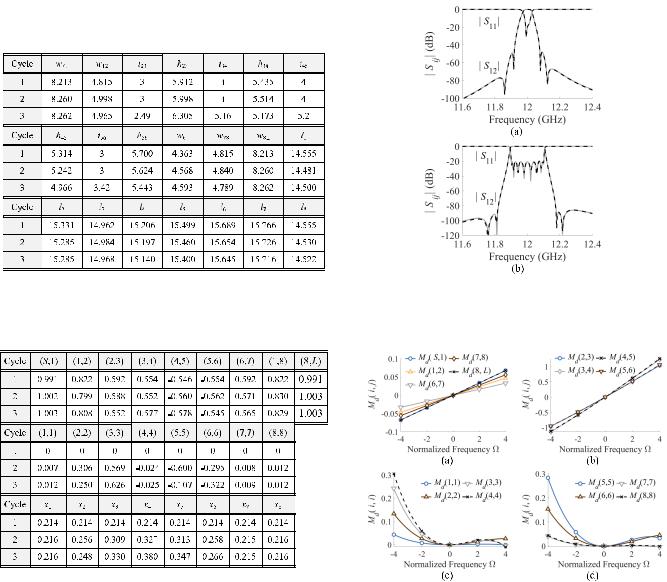
In [13], a resonant coupling iris with two fanlight windows was proposed to introduce one TZ in an inline filter structure. Such a dispersive coupling structure is adopted in designing a four-pole waveguide filter in this example. Two resonant irises are placed between resonators 2 and 3, and resonators 3 and 4 to generate two TZs, one in the lower and the other in the higher rejection bands. To begin with, the resonant coupling irises are roughly EM designed with their zero-crossing coupling occurring at the desired TZs and other dimensions of the filter complying with the initially synthesized M0 with the center frequency f0 = 11 GHz, the bandwidth BW = 200 MHz, and the return loss RL = 23 dB, without considering any dispersion effect. The synthesized initial M0 is listed in Table I. In this design example, WR75 waveguide (a = 19.05 mm and b = 9.525 mm) is used for the resonators and the interfacing waveguide.
Fig. 5(a) shows the front view of the resonant iris structure. The impedance inverter K versus frequency with respect to different dimensions of the iris structure is shown in Fig. 5(b)–(e), demonstrating the relationship of the dispersion characteristics and the dimensions of the resonant iris. It can be seen that by controlling h2, the inverter K at the center frequency can be changed independently, whereas dimensions h1 and w2 dominate the slope of the coupling value versus frequency. Having said that, M0 can be relatively independent of an extracted Md ( ).
Using the design formula in [8], the reactance slopes in cycle 1 are calculated by (18), and are listed in Table I,
Fig. 5. (a) Dimensions of the resonant |
iris. (b)–(e) Impedance inverter |
K versus (b) width of upper window w1, |
(c) height of upper window h1, |
(d) width of lower window w2, and (e) height of lower window h2.
Fig. 6. (a) Physical model of the four-pole dispersive waveguide filter with two resonant irises. (b) Top and side views of the filter with dimensions.
since (15) cannot be applied without the information of the dispersive characteristic. By adjusting w1, h1, w2, and h2 of the two resonant irises, coupling elements for M0(2,3) and M0(3,4) can be realized with the design formulas (1) through (4), (16), and (17). Note that M0(2,3) is set to a negative value, because its zero-crossing frequency is in the higher rejection band. The filter dimensions to be designed are marked in Fig. 6(b). Initially designed dimensions in cycle 1 are listed in Table II. The filter responses according to the DCM M( ) = M0 + Md ( ), and that of the EM simulation are shown in Fig. 7. A good agreement between the EM simulated response and that of the DCM validates the extracted circuit model introduced in Section II. The response is not equal-rippled, because the synthesized M0 does not incorporate the dispersion effect. As shown in Fig. 8(a), the
Authorized licensed use limited to: Newcastle University. Downloaded on May 18,2020 at 02:55:23 UTC from IEEE Xplore. Restrictions apply.

ZHANG et al.: DIRECT SYNTHESIS AND DESIGN OF DISPERSIVE WAVEGUIDE BANDPASS FILTERS |
1683 |
TABLE II
DIMENSIONS OF THE FOUR-POLE WAVEGUIDE FILTER IN TWO
SYNTHESIS AND DESIGN CYCLES (UNIT: mm)
Fig. 7. Responses of the extracted DCM (solid lines) and the EM simulation (dashed lines) by μWave Wizard of cycle 1.
Fig. 9. Filter responses simulated by DCM (solid lines) and characteristic polynomials extracted from the DCM results (dashed lines) in each iteration for synthesizing M0 in the second design cycle of the four-pole filter.
TABLE III
M0 IN EACH ITERATION OF THE SECOND SYNTHESIS AND DESIGN
CYCLE OF THE FOUR-POLE WAVEGUIDE FILTER
Fig. 8. Frequency dependence of (a) sequential couplings Md (i,j) and
(b) self-couplings Md (i,i) in design cycle 2.
dispersion effect of the conventional coupling elements, such as Md (S,1), Md (1,2), and Md (4, L), is relatively weak. On the contrary, the two resonant couplings, namely Md (2,3) and Md (3,4), are strongly dispersive. In addition, Fig. 8(b) shows that the dispersion effect of self-couplings for the concerned dispersive resonators is quite nonlinear on the one hand, but is almost frequency-invariant in the vicinity of the center frequency, on the other hand. This observation supports the assumption in deriving the reactance slope in Section II.
In design cycle 2, reactance slopes can be updated using (15), as shown in Table I. By following the iterative synthesis procedure introduced in Section III, six iterations are taken to obtain the converged matrix M0. Note that P0(i) (s) = 1 for sequentially coupled filter is used in each iteration. Fig. 9 shows the responses simulated by the DCM and its corresponding characteristic polynomials extracted using MVF in each iteration. A slight discrepancy in the far ends of the rejection bands is mainly due to the higher order effect of the nonlinearity of the dispersion that could not be accurately modeled by the polynomials. The M0(i) and roots
of polynomials PD(i) (s) in each iteration in the design cycle are shown in Tables III and IV, respectively. It is seen that the dispersion effect generates not only two TZs near the passband, but also a far TZ.
Having had M0 for an equal-ripple response in the second design cycle, EM simulation for each coupling element at the center frequency is conducted to design the dimensions of both coupling elements and resonator lengths. In designing the dimensions for the dispersive coupling elements to meet the synthesized M0(2,3) and M0(3,4) while retaining the dispersion Md (2,3) and Md (3,4), h2 is taken as the tuning dimension. The designed filter dimensions at the end of the second design cycle are also listed in Table II. A photograph of the prototyped filter is shown in Fig. 10 (a) and the actual 3-D model is shown in Fig. 10 (b), which is slightly different from the EM designed model in that round corners of resonators and the E-plane bends at the two ports are introduced for the convenience of
Authorized licensed use limited to: Newcastle University. Downloaded on May 18,2020 at 02:55:23 UTC from IEEE Xplore. Restrictions apply.

1684 IEEE TRANSACTIONS ON MICROWAVE THEORY AND TECHNIQUES, VOL. 68, NO. 5, MAY 2020
TABLE IV
ROOTS OF THE CHARACTERISTIC POLYNOMIALS P |
(i) |
(s) AND |
(i) |
OF THE |
|
D |
|
0 |
|
SIX ITERATIONS IN THE SECOND SYNTHESIS AND DESIGN CYCLE
Fig. 10. (a) Photograph of the prototyped waveguide filter with two resonant irises. (b) Isometric model of the prototyped filter.
Fig. 12. (a) Dimensions of the resonant iris with an offset partial height post. Impedance inverter K versus (b) post height h, and (c) offset t with d = 1.5 mm.
Fig. 13. (a) Isometric view of the eight-pole waveguide filter with four partial height post coupling elements. (b) Top and side views of the filter with dimensions.
Fig. 11. Responses by EM simulation using μWave Wizard (dashed lines), by the synthesized DCM (solid lines), and by measurement (dotted blue lines).
manufacturing. Since the bends are well-matched, so that the filter response is not affected. The impact of the round corners is also very weak and can be compensated by tuning screws. Fig. 11 shows the responses by the synthesized DCM, μWave EM simulation, and measurement. A good agreement of the three responses affirms the proposed dimensional synthesis and design method.
B. Eight-Pole Waveguide Filter Using Partial Height Posts
Coupling Elements
There are many ways to create dispersive coupling elements. An offset partial height post can also introduce a TZ in a rectangular waveguide filter. In [14], such a dispersive coupling element, as shown in Fig. 12(a), was referred as
a band-reject element, and its dimensions were designed by optimization.
In this design, for example, the offset post is considered as a dispersive coupling element with a strong dispersion. The eight-pole waveguide filter with four partial height posts, each generating one TZ, is directly synthesized and EM designed by applying the proposed dimensional design method. The center frequency of the filter f0 = 12 GHz and the bandwidth BW = 200 MHz. WR75 waveguide is used for the resonators and interfacing waveguides.
As is claimed in [14] that the location of the TZ is primarily determined by the height of the post. It can be observed from Fig. 12(b) and (c) that the K value at the center frequency and its zero-crossing frequency, or TZ frequency, are jointly determined by the height h and the offset t. However, the dimension t dominantly controls the slope of the dispersion characteristic, which contributes to Md ( ), whereas the dimension h affects the inverter value K at the center frequency heavily, and in turn determines M0.
The structure of the eight-pole waveguide filter is shown in Fig. 13(a), where four partial height post coupling elements are used to realize M23, M34, M45, and M56 and to introduce four TZs at 11.7, 11.85, 12.15, and 12.2 GHz, respectively. The dimensional variables are marked in Fig. 13(b), whose values in each design cycle are listed in Table V.
Authorized licensed use limited to: Newcastle University. Downloaded on May 18,2020 at 02:55:23 UTC from IEEE Xplore. Restrictions apply.
ZHANG et al.: DIRECT SYNTHESIS AND DESIGN OF DISPERSIVE WAVEGUIDE BANDPASS FILTERS |
1685 |
TABLE V
DIMENSIONS OF THE EIGHT-POLE WAVEGUIDE FILTER IN THREE
SYNTHESIS AND DESIGN CYCLES WITH d = 1.5 mm (UNIT: mm)
TABLE VI
SYNTHESIZED M0 AND REACTANCE SLOPES OF THE EIGHT-POLE WAVEGUIDE FILTER IN THREE SYNTHESIS AND DESIGN CYCLES
In design cycle 1, the traditional synthesis method is used to obtain M0 with 20-dB return loss, which is listed in Table VI. According to the M0 and the reactance slopes obtained by (18), an initial dimension can be designed by EM simulation of individual partial height post coupling element with different offsets t and heights h, and is listed in Table V. Responses of the circuit model and the EM model of the initial design are superposed in Fig. 14(a). With the initial design, reactance slope parameters are updated in Table VI.
Using the procedure given in Section III and the dispersion characteristics Md ( ) extracted in design cycle 1, M0 that targets an equal-ripple response is obtained in design cycle 2 and is listed in Table VI. By adjusting height h while keeping offset t unchanged to realize the required couplings in M0, the dimension design can be done without changing Md ( ) too much in design cycle 2. At the end of the design cycle, reactance slope parameters are also updated for the next design cycle.
The responses of the DCM M0 + Md ( ) and the EM simulation after design cycle 2 are superimposed in Fig. 14(b),
Fig. 14. Responses of the M0 + Md ( ) (solid lines) and the EM simulation (dashed lines) in (a) design cycle 1 and (b) design cycle 2 of the eight-pole inline waveguide filter.
Fig. 15. Dispersion characteristic Md ( ) of (a) and (b) mutual couplings Md (i,j) and (c) and (d) self-couplings Md (i,i) in design cycle 2 of the eight-pole inline waveguide filter.
showing equal-ripple responses. A very good agreement between the responses of the circuit and EM models justifies that the dispersion characteristics are not changed noticeably in the design cycle. In design cycle 2, the extracted dispersion characteristics Md ( ), as shown in Fig. 15(a)–(d), are used. Obviously, the dispersion for the partial height post coupling elements is much larger than that of regular H-plane window irises.
However, the final locations of the TZs are determined not only by the dispersion characteristics of inter-resonator couplings, but also by those of the self-couplings of resonators. To achieve the designated TZs accurately, the offset dimensions of the four posts are fine-tuned to slightly alter Md ( ), as shown in Fig. 16. Basically, the greater the slope of dispersive mutual coupling is, the closer to the passband the TZ would be. After a few trial and errors, the offset t for each
Authorized licensed use limited to: Newcastle University. Downloaded on May 18,2020 at 02:55:23 UTC from IEEE Xplore. Restrictions apply.

1686 |
IEEE TRANSACTIONS ON MICROWAVE THEORY AND TECHNIQUES, VOL. 68, NO. 5, MAY 2020 |
Fig. 16. Updated dispersion characteristic Md ( ) of (a) mutual couplings |
Fig. 18. Response of the M0 + Md ( ) (solid lines) and the EM simulation |
Md (i,j) and (b) self-couplings Md (i,i) in design cycle 3 of the eight-pole inline |
|
waveguide filter. |
(dashed lines) in design cycle 3 of the eight-pole inline waveguide filter. |
|
Fig. 17. Responses simulated by DCM (solid lines) and characteristic polynomials extracted from the DCM results by MVF (dashed lines) in each iteration for synthesizing M0 in the design cycle 3 of the eight-pole filter example, where the red line represents the return loss spec.
dispersive coupling element is tuned to realize the intended TZs in design cycle 3. The iterative synthesis process in cycle 3 is shown in Fig. 17 with the spec line for return loss marked in a red line. The final synthesized M0 is listed in Table VI, and the designed dimensions are listed in Table VII. The simulated responses of the circuit model M0 + Md ( ) and μWave EM model at the end of design cycle 3 are shown in Fig. 18, showing equal-ripple responses with desired TZs.
In summary, design cycle 1 basically provides an initial dimensional design for the extraction of dispersive characteristics. A dimensional design for an equal-ripple response is realized in design cycle 2. The last design cycle is conducted for fine-tuning of TZs by adjusting the dimension of a dispersive coupling element that controls the slope of the dispersive characteristic. Basically, the desired out-of-band response is controlled by adjusting Md ( ), and the equal-ripple in-band behavior is maintained by achieving an appropriate M0 as long as Md ( ) and M0 can be controlled independently.
V. DISCUSSION ON CONVERGENCE
With the proposed iterative synthesis method, good convergence can be obtained for most of the cases, except two scenarios: 1) Md ( ) exhibits a very large variation versus frequency and 2) the required return loss level is difficult to meet. For the first scenario, a penalty factor γ (which is less than 1) can be multiplied to Md ( ) to obtain a temporary M0 corresponding to a virtual dispersion γ Md ( ), and this temporary M0 can be further used as a better starting point to obtain the final M0 with actual Md ( ). This relaxation means that a converged solution can always be obtained if it exists. When the solution does not exist, or for the second scenario, the imposed return loss level should be relaxed, such that an optimal M0 can be obtained for the given Md ( ) with an equal-ripple response.
VI. CONCLUSION
A dimensional filter synthesis and design framework is proposed for directly designing a narrowband waveguide filter with strong dispersive coupling elements. For given dispersion characteristics of some specific coupling structures in an inline waveguide filter, the coupling matrix that ensures an equal-ripple response can be directly synthesized. The synthesized coupling allows the dimensional design to be done by EM simulation of each coupling element at the center frequency. Two demonstrating examples are given to illustrate the procedure of extracting a DCM and the proposed iterative synthesis process for the constant coupling matrix. Both examples are very well verified by either hardware prototyping or μWave EM simulation. The proposed synthesis and design framework is an attempt toward synthesizing a microwave filter with the physical identity of its realization.
ACKNOWLEDGMENT
The authors would like to thank Dr. S. Yin of Pivotone Communication Technologies for fabricating the hardware in
Authorized licensed use limited to: Newcastle University. Downloaded on May 18,2020 at 02:55:23 UTC from IEEE Xplore. Restrictions apply.

ZHANG et al.: DIRECT SYNTHESIS AND DESIGN OF DISPERSIVE WAVEGUIDE BANDPASS FILTERS |
1687 |
this article. They also like to thank M. GmbH for providing the complimentary copy of μWave Wizard software for the research.
REFERENCES
[1] H. A. Wheeler, “Band-pass filter, including trap circuits,” U.S. Patent 2 247 898, Jul. 1, 1941.
[2] |
J. D. Rhodes, “A low-pass prototype network for microwave linear |
|
|
phase filters,” IEEE Trans. Microw. Theory Techn., vol. MTT-18, no. 6, |
|
|
pp. 290–300, Jun. 1970. |
|
[3] |
R. J. Cameron, “Fast generation of Chebyshev filter |
prototypes |
|
with asymmetrically-prescribed transmission zeros,” ESA |
J., vol. 6, |
pp. 83–95, Jan. 1982.
[4]A. E. Atia, A. E. Williams, and R. W. Newcomb, “Narrowband multiple-coupled cavity synthesis,” IEEE Trans. Circuits Syst., vol. CAS-21, no. 5, pp. 649–655, Sep. 1974.
[5]R. J. Cameron, “General coupling matrix synthesis methods for Chebyshev filtering functions,” IEEE Trans. Microw. Theory Techn., vol. 47, no. 4, pp. 433–442, Apr. 1999.
[6]R. F. Baum, “Design of unsymmetrical band-pass filters,” IRE Trans. Circuit Theory, vol. 4, no. 2, pp. 33–40, Jun. 1957.
[7]P. Zhao and K.-L. Wu, “Adaptive computer-aided tuning of coupled-resonator diplexers with wire T-junction,” IEEE Trans. Microw. Theory Techn., vol. 65, no. 10, pp. 3856–3865, Oct. 2017.
[8]L. Q. Bui, D. Ball, and T. Itoh, “Broadband millimeter-wave E-plane bandpass filters,” IEEE Trans. Microw. Theory Techn., vol. MTT-32, no. 12, pp. 1655–1658, Dec. 1984.
[9]H. Hu and K.-L. Wu, “A deterministic EM design technique for general waveguide dual-mode bandpass filters,” IEEE Trans. Microw. Theory Techn., vol. 61, no. 2, pp. 800–807, Feb. 2013.
[10]S. Amari, M. Bekheit, and F. Seyfert, “Notes on bandpass filters whose inter-resonator coupling coefficients are linear functions of frequency,” in IEEE MTT-S Int. Microw. Symp. Dig., Jun. 2008, pp. 1207–1210.
[11]M. Ohira, Z. Ma, H. Deguchi, and M. Tsuji, “A novel coaxial-excited FSS-loaded waveguide filter with multiple transmission zeros,” in Proc. Asia–Pacific Microw. Conf., Dec. 2010, pp. 1720–1723.
[12]M. Politi and A. Fossati, “Direct coupled waveguide filters with generalized Chebyshev response by resonating coupling structures,” in Proc. Eur. Microw. Conf. (EuMC), Sep. 2010, pp. 966–969.
[13]U. Rosenberg, S. Amari, and F. Seyfert, “Pseudo-elliptic direct-coupled resonator filters based on transmission-zero-generating irises,” in Eur. Microw. Conf. Dig., Sep. 2010, pp. 962–965.
[14]U. Rosenberg and S. Amari, “A novel band-reject element for pseudoelliptic bandstop filters,” IEEE Trans. Microw. Theory Techn., vol. 55, no. 4, pp. 742–746, Apr. 2007.
[15]S. Shin and R. V. Snyder, “At least N+1 finite transmission zeros using frequency-variant negative source-load coupling,” IEEE Microw. Wireless Compon. Lett., vol. 13, no. 3, pp. 117–119, Mar. 2003.
[16]L. Szydlowski, A. Lamecki, and M. Mrozowski, “Coupled-resonator filters with frequency-dependent couplings: Coupling matrix synthesis,”
IEEE Microw. Wireless Compon. Lett., vol. 22, no. 6, pp. 312–314, Jun. 2012.
[17]L. Szydlowski, N. Leszczynska, and M. Mrozowski, “Dimensional synthesis of coupled-resonator pseudoelliptic microwave bandpass filters with constant and dispersive couplings,” IEEE Trans. Microw. Theory Techn., vol. 62, no. 8, pp. 1634–1646, Aug. 2014.
[18]L. Szydlowski, A. Lamecki, and M. Mrozowski, “A novel coupling matrix synthesis technique for generalized Chebyshev filters with resonant source–load connection,” IEEE Trans. Microw. Theory Techn., vol. 61, no. 10, pp. 3568–3577, Oct. 2013.
[19]Y. Zhang, H. Meng, and K.-L. Wu, “Synthesis of microwave filters with dispersive coupling using isospectral flow method,” in IEEE MTT-S Int. Microw. Symp. Dig., Jun. 2019, pp. 846–848.
[20]G. Li, “Coupling matrix optimization synthesis for filters with constant and frequency-variant couplings,” PIER Lett., vol. 82, pp. 73–80, Feb. 2019.
[21]S. Tamiazzo and G. Macchiarella, “Synthesis of cross-coupled filters with frequency-dependent couplings,” IEEE Trans. Microw. Theory Techn., vol. 65, no. 3, pp. 775–782, Mar. 2017.
[24]L. Szydlowski, N. Leszczynska, and M. Mrozowski, “Generalized Chebyshev bandpass filters with frequency-dependent couplings based on stubs,” IEEE Trans. Microw. Theory Techn., vol. 61, no. 10,
pp.3601–3612, Oct. 2013.
[25]R. Das, Q. Zhang, A. Kandwal, and H. Liu, “All passive realization of lossy coupling matrices using resistive decomposition technique,” IEEE Access, vol. 7, pp. 5095–5105, 2019.
[26]S. B. Cohn, “Direct-coupled-resonator filters,” Proc. IRE, vol. 45, no. 2,
pp.187–196, 1957.
[27]G. L. Matthaei, L. Young, and E. M. T. Jones, Microwave Filters, Impedance-matching Networks, and Coupling Structures. New York, NY, USA: McGraw-Hill, 1964.
[28]P. Zhao and K.-L. Wu, “Model-based vector-fitting method for circuit model extraction of coupled-resonator diplexers,” IEEE Trans. Microw. Theory Techn., vol. 64, no. 6, pp. 1787–1797, Jun. 2016.
[29]μWave Wizard. Version 8.1, Mician GmbH, Bremen, Germany, 2011.
Yan Zhang (Student Member, IEEE) received the B.S. degree in electronic engineering from the University of Electronic Science and Technology of China, Chengdu, China, in 2017. She is currently pursuing the Ph.D. degree at The Chinese University of Hong Kong, Hong Kong.
Her current research interests include synthesis and robot automatic tuning algorithms for filters with strong dispersion and filers with irregular topology.
Ms. Zhang was a recipient of Hong Kong Ph.D. Fellowship.
Huan Meng received the B.Eng. degree (Hons.) in electronic and information engineering from The Hong Kong Polytechnic University, Hong Kong, in 2010, and the M.Phil. and Ph.D. degree in electronic engineering from The Chinese University of Hong Kong, Hong Kong, in 2012 and 2019, respectively.
He is currently working as a Microwave Engineer with Mechawaves Manufacturing Ltd. His research is mainly focused on the design, synthesis, and tuning of passive microwave coupled-resonator
networks, including diplexers and multiplexers.
Ke-Li Wu (Fellow, IEEE) received the B.S. and M.Eng. degrees from the Nanjing University of Science and Technology, Nanjing, China, in 1982 and 1985, respectively, and the Ph.D. degree from Laval University, Quebec, QC, Canada, in 1989.
From 1989 to 1993, he was a Research Engineer with McMaster University, Hamilton, ON, Canada. He joined the Corporate Research and Development Division, COM DEV (now Honeywell Aerospace), Cambridge, ON, Canada in 1993, where he was a Principal Member of Technical Staff. Since 1999,
he has been with The Chinese University of Hong Kong, Hong Kong, where he is currently a Professor and the Director of the Radio Frequency Radiation Research Laboratory. His current research interests include EM-based circuit domain modeling of high-speed interconnections, robot automatic tuning of
[22]Y. He et al., “A direct matrix synthesis for in-line filters with transmicrowave filters, decoupling techniques of MIMO antennas, and Internet of mission zeros generated by frequency-variant couplings,” IEEE Trans. Things technologies.
Microw. Theory Techn., vol. 66, no. 4, pp. 1780–1789, Apr. 2018.
[23]Y. He, G. Macchiarella, Z. Ma, L. Sun, and N. Yoshikawa, “Advanced direct synthesis approach for high selectivity in-line topology filters comprising N—1 Adjacent frequency-variant couplings,” IEEE Access, vol. 7, pp. 41659–41668, 2019.
Prof. Wu is a member of the IEEE MTT-8 Subcommittee. He serves as a TPC member for many prestigious international conferences. He was a recipient of the 1998 COM DEV Achievement Award and the Asia–Pacific Microwave Conference Prize twice in 2008 and 2012, respectively. He was an Associate Editor of the IEEE TRANSACTIONS ON MTT from 2006 to 2009.
Authorized licensed use limited to: Newcastle University. Downloaded on May 18,2020 at 02:55:23 UTC from IEEE Xplore. Restrictions apply.