

диафрагмированные волноводные фильтры / b5cf1bc8-3ac8-479f-a0be-9b88a9b105c3
.pdfThis article has been accepted for inclusion in a future issue of this journal. Content is final as presented, with the exception of pagination.
IEEE TRANSACTIONS ON MICROWAVE THEORY AND TECHNIQUES |
1 |
Stubbed Waveguide Cavity Filters
Simone Bastioli , Senior Member, IEEE, and Richard V. Snyder
 , Life Fellow, IEEE
Abstract— A new class of reduced-size waveguide filters implementing pseudoelliptic filtering functions is presented in this article. The basic structure of these filters is the stubbed waveguide cavity (SWC), which is proposed in both singleand double-stub configurations. The SWC consists of a main TE201 mode cavity, which is loaded with one or two E-plane stubs. The stubs behave as embedded half-mode cavities supporting additional resonant modes, and they are properly located so as to realize specific coupling schemes for the generation and control of transmission zeros. Depending on its configuration, a sole SWC can generate up to three poles and three transmission zeros. The design of higher order filters employing a cascade of SWCs, as well as combinations between SWCs and conventional waveguide cavities, are presented. The experimental results of a third-order filter employing one SWC (double-stub configuration) and a fifth-order filter employing two SWCs validate the feasibility of this new class of waveguide filters.
Index Terms— Cavities, elliptic functions, microwave filters, transmission zeros, waveguide.
I. INTRODUCTION
THE waveguide is the prime technology when high power handling capabilities and very low insertion losses are the leading requirements. In the higher portion of the microwave spectrum, antenna feeding systems typically employ complex waveguide assemblies, where filtering structures are key devices to ensure proper transmission and reception on certain
frequency channels [1], [2].
Rectangular, circular, or even elliptical cavities operating in certain TE or TM resonant modes are the basic elements for the design of waveguide filters. Conventionally, a waveguide cavity provides a single pole of resonance, and several cavities are usually cascaded to obtain higher order filters with steep transition bands. Waveguide cavities with enhanced capabilities can be obtained by employing established multi-mode approaches [3]–[6], as well as by adopting the more recent nonresonating mode techniques [7]–[12]. In both cases, a single cavity can provide multiple poles and/or transmission zeros, thus reducing the number of physical cavities that are needed to attain a certain rejection requirement.
Various cavity structures have been proposed over the years with the aim of realizing an increasing number of poles and transmission zeros. As far as rectangular cavities are concerned, some of the most effective implementations are
Manuscript received May 3, 2019; revised August 20, 2019; accepted September 13, 2019. This article is an expanded version from the IEEE MTT-S International Microwave Symposium (IMS), June 2–7, 2019, Boston, MA, USA. (Corresponding author: Simone Bastioli.)
The authors are with RS Microwave, Butler, NJ 07405 USA (e-mail: sbastioli@rsmicro.com; r.snyder@ieee.org).
Color versions of one or more of the figures in this article are available online at http://ieeexplore.ieee.org.
Digital Object Identifier 10.1109/TMTT.2019.2944358
reported in [6]–[11]: the cavities proposed in [7] and [8] are each capable of generating one pole and one transmission zero; the cavity proposed in [6] can generate two poles and a transmission zero at the expense of virtually doubling the cavity size; finally, the cavity proposed in [9]–[11] can generate two poles and two transmission zeros at the expense of a more complex arrangement requiring advanced design capabilities. For further enhancing the capabilities provided by a single cavity structure, a new type of waveguide cavity, namely, the stubbed waveguide cavity (SWC), has been recently introduced in [13]. In contrast with other techniques [14]–[16] where the stubs are essentially implementing frequency selective coupling elements (each stub is associated to a coupling element and can generate one transmission zero), the stubs employed in the SWC are directly embedded into the cavities, thus enhancing the order (both poles and transmission zeros) of the main cavity where they belong. The structure proposed in [13] has proven indeed effective in realizing up to three poles and three transmission zeros, although no design guidelines or actual multiple cavity filters have been presented.
In order to generalize and fulfill the potentials of this new technique for the design of reduced-size multiple cavity elliptic filters, this article significantly expands the concepts introduced in [13]. The SWC is proposed in two different arrangements, namely singleand double-stub configurations, each having its own advantages and applications. Although requiring complex design techniques based on extensive optimization procedures, some guidelines for the design and physical dimensioning of these cavities are explained in detail. For the same purpose, the application of a multi-port optimization technique (originally proposed in [17] for more conventional waveguide cavities) has proven to be extremely effective in facilitating the design of these structures. The design of higher order filters employing a cascade of SWCs, as well as combinations of SWCs and conventional waveguide cavities, are also presented in this article. Finally, the experimental results of two manufactured prototypes validate the feasibility of this new class of SWC filters.
II. SINGLE-STUB CONFIGURATION
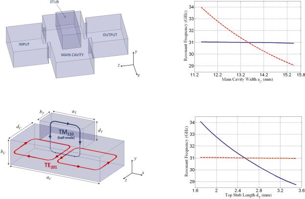
The SWC in the single-stub configuration consists of a main TE201 mode cavity which is loaded with an E-plane waveguide stub. The cavity structure (including the feeding input and output waveguides) is shown in Fig. 1. The rectangular parallelepiped stub emerges from the top wall of the waveguide and is oriented along the width of the main cavity (stub broad wall parallel with the x-axis). Such an E-plane stub behaves as an embedded half-mode cavity supporting a TM110, the latter being in addition to the main cavity TE201 mode. The magnetic
0018-9480 © 2019 IEEE. Personal use is permitted, but republication/redistribution requires IEEE permission. See http://www.ieee.org/publications_standards/publications/rights/index.html for more information.
This article has been accepted for inclusion in a future issue of this journal. Content is final as presented, with the exception of pagination.
2
Fig. 1. SWC in single-stub configuration (input and output waveguides are included).
Fig. 2. Magnetic field patterns of the resonant modes inside an SWC in single-stub configuration.
fields of the two modes are depicted in Fig. 2. The stub is always located at the center of the main cavity length (at dC /2), where no coupling can occur between the TM110 mode in the stub and the TE201 mode in the main cavity.
The resonant frequencies of the modes can be controlled almost independently by the dimensions of certain structural parameters. The TE201 mode resonant frequency f201 is controlled by the width aC and length dC of the main cavity. An initial dimensioning of the main cavity can be carried out by using the well-known equation
|
|
|
|
|
|
|
|
|
|
|
|
|
|
f201 |
|
c |
|
2π |
|
2 |
|
π |
|
2. |
(1) |
||
= |
2π |
aC |
|
|
+ dC |
|
|||||||
|
|
|
|
|
|
||||||||
The resonant frequency f110 of the TM110 mode depends primarily on the length dT and width aT of the top stub. The height bT of the stub primarily determines the unloaded Q-factor and power handling capability of its resonant mode. In practice, the width and height of the stub can be set beforehand (standard waveguide cross sections or similar are convenient choices to guarantee high Q-factor and power handling performances), while the length is used to control the resonant frequency. As a first approximation, the stub length can be initially set to a quarter of the guided-wavelength (halfmode approximation).
However, due to the loading effect of the main cavity upon the stub (at the transition between stub and cavity, along the y-axis), as well as the loading effect of the stub on the main cavity mode, a full-wave simulator must be employed to properly dimension and optimize the SWC structure according to
IEEE TRANSACTIONS ON MICROWAVE THEORY AND TECHNIQUES
Fig. 3. Resonant frequencies of the modes (TE201 dashed red curve, TM110 solid blue curve) versus the main cavity width aC (bC = 3.556 mm, dC = 6.807 mm, aT = 6.580 mm, bT = 3.556 mm, and dT = 2.537 mm).
Fig. 4. Resonant frequencies of the modes (TE201 dashed red curve, TM110 solid blue curve) versus the top stub length dT (aC = 13.530 mm, bC = 3.556 mm, dC = 6.807 mm, aT = 6.580 mm, and bT = 3.556 mm).
the desired resonant frequencies. As an example, the structure in Fig. 2 yields f201 = f110 = 31 GHz (Ansys HFSS, eigenmode solver) for the following dimensions: aC = 13.530 mm,
bC |
= 3.556 mm, dC = 6.807 mm, aT = 6.580 mm, |
bT |
= 3.556 mm, and dT = 2.537 mm. The computed |
unloaded Q-factors (ideal silver surfaces) are 5050 for the TE201 mode, and 4500 for the TM110 mode (for reference, a conventional TE101 mode cavity in WR-28 at 31 GHz has an unloaded Q-factor of 4700). Concerning the spurious performance, the first spurious higher order mode for this cavity is located at 39 GHz.
In order to demonstrate the independency of the resonant modes with respect to the structural parameters, Figs. 3 and 4 show the computed resonant frequencies versus aC and dT , respectively, as expected, f201 changes with aC ( f110 remains almost constant), whereas f110 changes with dT ( f201 remains almost constant). Observe that such an independency holds obviously true also for the other cavity and stub dimensions: specifically, the main cavity length dC does not affect the TM110 mode in the stub, while the stub width aT does not affect the TE201 mode in the main cavity.
The sensitivity of the modes with respect to manufacturing imperfections affecting aC and dT can be derived from the slopes (around 31 GHz) of the curves in Figs. 3 and 4: the TE201 mode has a sensitivity of −1.18 MHz/um with respect to aC while the TM110 mode has a sensitivity of −3.01 MHz/um with respect to dT (for reference, a conventional TE101 mode

This article has been accepted for inclusion in a future issue of this journal. Content is final as presented, with the exception of pagination.
BASTIOLI AND SNYDER: SWC FILTERS |
3 |
Fig. 5. Equivalent topology of the SWC in single-stub configuration.
Fig. 7. Coupling matrix response and HFSS simulation (lossless) of the designed SWC.
Fig. 6. Structural parameters of an SWC in single-stub configuration.
in a WR-28 cavity resonating at 31 GHz has a sensitivity of −2.52 MHz/um with respect to the cavity length).
The modes of the SWC can be excited at the input and output by means of simple inductive irises, as shown in the structure of Fig. 1. The location of the input/output irises with respect to the main cavity is properly designed so that the TE201 and the TM110 modes are both excited by the feeding waveguides’ fundamental mode. To this purpose, the irises are always offset with respect to the cavity center.
The resulting coupling scheme is a doublet topology, as depicted in Fig. 5. Observe that the negative coupling on the left side of the TE201 mode represents the 180◦ phase difference at the output port between this mode and the TM110 mode. The direct coupling between the input and output (dashed line between source and load) represents the contribution of the nonresonating TE10 mode, which is bypassing the resonant modes inside the cavity. In contrast with all the other coupling coefficients, such an input-to-output coupling cannot be fully exploited as an operative degree of freedom for design purposes. As a result, although the topology in Fig. 6 and the corresponding SWC structure do generate filtering functions with two poles and two transmission zeros, only one of the transmission zeros can be fully controlled with high design flexibility. In fact, by properly dimensioning certain structural parameters, one transmission zero can be located extremely close to the passband edges, while the second transmission zero is always located above the passband at a relatively farther distance (partial control of the second transmission zero location).
As far as the location of the close transmission zero is concerned, this can be located either below or above the passband depending on the difference between the resonant frequencies of the two resonant modes. In particular, if the TE201 mode (whose input/output coupling is commonly weaker) resonates below the TM110 mode (whose input/output coupling is commonly stronger), then the transmission zero will be generated on the lower passband edge; on the other hand, the transmission zero will appear in the upper edge of the passband when the TE201 mode resonates above the TM110 mode.
As an example, Fig. 7 shows the full-wave simulation (Ansys HFSS) of an SWC in single-stub configuration designed according to the following normalized coupling matrix ( f0 = 31 GHz, w = 2.25%):
|
0.971 |
|
1.274 |
|
0 |
0.971 |
|
|
0 |
0.971 |
0.502 |
0.090 |
|
||
M = |
0.502 |
− |
0 |
1.371 |
−0.502 |
. |
|
|
0.090 |
0.971 |
− |
0.502 |
0 |
|
|
|
|
|
|
|
|
|
|
Observe that since M22 > M11, the close transmission zero is located on the lower edge of the passband. With reference to Fig. 6, the dimensions of the optimized structure are the following: a = 7.112 mm, b = bC = 3.556 mm,
iI |
= iO = 4.013 mm, aC = 13.335 mm, dC = |
6.858 mm, |
aT |
= 6.604 mm, bT = 3.556 mm, dT = 1.9812 mm, and |
|
pI |
= pO = pT = 1.397 mm; the thickness |
of the iris |
is 0.508 mm. The agreement between the full-wave simulation and the coupling matrix response validates the topology in Fig. 5 and the theorized coupling mechanisms among various modes.
The main structural design parameters to control and physically realize the various coupling coefficients are the dimension and location of the input and output irises, as well as the location of the stub with respect to the main cavity width. The dimension of the input iris iI is used to increase or decrease at the same time both coupling JS1 and JS2 (as well as obviously JSL), while the offset pI of the iris with respect
This article has been accepted for inclusion in a future issue of this journal. Content is final as presented, with the exception of pagination.
4 |
IEEE TRANSACTIONS ON MICROWAVE THEORY AND TECHNIQUES |
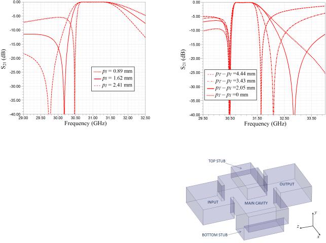
Fig. 8. Simulated response (S21) of three cavities optimized for different positions of the input and output irises ( pI = pO ).
Fig. 9. Simulated responses (S21) of four cavities optimized for different positions of the top stub ( pT ) with respect to the position of the input and output irises ( pI = pO ).
to the center of the main cavity width is effectively used to change the ratio between JS1 and JS2. The same considerations hold true for the output iris dimensions and the coupling J1L and J2L . The dimensions of the input and output irises will, therefore, be exploited to control the overall bandwidth of the filtering function. On the other hand, the ability to alter the ratio JS1/JS2 at the input and J1L /J2L at the output thanks to the offsets pI and pO is the key to control the distance between the close transmission zero and the passband edges. Fig. 8 shows the responses of three cavities optimized for various values of the input and output offsets (in these examples pI = pO ): as the offsets decreases, the transmission zero moves closer to the passband edge. As a result, filtering function with an extremely close transmission zero can be realized using very small offsets.
Although restricted to the upper stopband, the location of the second (farther) transmission zero (whose generation is ascribed to the direct-coupling JSL) can be partially controlled. Observe that in order to move this transmission zero below the passband, the sign of JSL should be inverted, which is practically not possible with the proposed configuration. The magnitude of JSL is proportional to the dimensions of the irises, the latter being already exploited to control the other characteristics of the filtering function. However, the ratio JS1/JSL (and J1L /JSL) can be altered by adjusting the location pT of the top stub. In practice, such a ratio controls the distance between the second transmission zero and the upper edge of the passband. If the stub is near to the input and output irises ( pI − pT 0), then the ratio JS1/JSL is maximized, and the resulting transmission zero will fall relatively far in the upper stopband. On the other hand, as the stub gets farther away from the input and output irises, JS1 decreases while JSL increases, thus significantly moving the second transmission zero closer to the upper edge of the passband. Such control over the second transmission zero is demonstrated in Fig. 9, where the responses of four cavities optimized for various values of the stub position pT are plotted.
Fig. 10. SWC in double-stub configuration (input and output waveguides are included).
III. DOUBLE-STUB CONFIGURATION
Compared to the single-stub arrangement, the SWC in the double-stub configuration is loaded with a second E-plane stub. The cavity structure (including the feeding input and output waveguides) is shown in Fig. 10. The second stub emerges from the bottom wall of the waveguide and is oriented along the length of the main cavity (stub broad wall parallel with the z-axis). Similar to the top stub, the bottom stub behaves as another embedded half-mode cavity supporting a TE011 mode which is in addition to the TE201 and TM110 modes. Since the two stubs are orthogonally oriented, the TM110 and the TE011 modes are always isolated with respect to each other. The magnetic fields of the three modes are depicted in Fig. 11. In contrast with the top stub (whose TM110 is never coupled to the TE201 mode), the position pB of the bottom stub with respect to the main cavity sidewall must be properly dimensioned in order to control the intra-coupling between the TE011 mode and the TE201 mode. Such an intracoupling can be eliminated by properly adjusting pB at around quarterwavelength.
The resonant frequency of the TE011 mode depends primarily on the length dB and width aB of the bottom stub. Once the width is set, the length is used to control the resonant

This article has been accepted for inclusion in a future issue of this journal. Content is final as presented, with the exception of pagination.
BASTIOLI AND SNYDER: SWC FILTERS |
5 |
Fig. 13. Equivalent topology of the SWC in double-stub configuration.
Fig. 11. Magnetic field patterns of the resonant modes inside an SWC in double-stub configuration.
Fig. 12. Resonant frequencies of the modes (TE201 dashed red curve, TM110 solid blue curve, TE011 dotted green curve) versus the bottom stub length dB
(aC = 13.400 mm, bC = 3.556 mm, dC = 7.070 mm, aT = 6.550 mm, bT = 3.556 mm, dT = 2.375 mm, aB = 6.500 mm, bB = 3.300 mm, and pB = 3.740 mm).
frequency. As mentioned for the top stub in Section II, the length of the bottom stub can be initially set to a quarter of the guided-wavelength (half-mode approximation) before conducting a full-wave optimization of the whole structure to compensate for the various mutual loading effects. As an example, the structure in Fig. 11 yields f011 = f201 =
= 31 GHz (Ansys HFSS, eigenmode solver) for the following dimensions: aC = 13.400 mm, bC = 3.556 mm, dC = 7.070 mm, aT = 6.550 mm, bT = 3.556 mm, dT = 2.375 mm, aB = 6.500 mm, bB = 3.300 mm, dB = 2.74 mm, and pB = 3.740 mm. The computed unloaded Q-factors (ideal silver surfaces) are 5200 for the TE201 mode, 4300 for the TM110 mode, and 4400 for the TE011 mode. Concerning the spurious performance, the first spurious higher order mode for this cavity is located at 39.4 GHz.
As far as the independency of the resonant modes is concerned, Fig. 12 shows the computed resonant frequency of the TE011 mode versus dB : f011 changes with dB while f110 and f201 remain constant, thus proving the possibility of having independent control over the resonant mode of the bottom stub.
Similar to the single-stub configuration, the input and output waveguides are coupled at the same time to the TE201 and
TM110 mode by means of simple inductive irises in the offset position. In order to avoid any potential spurious coupling between the input/output and the TE011 mode, the offset of the irises is always directed away from the side where the bottom stub is located. The TE011 in the bottom stub is meant to be coupled only with the TE201 of the main cavity, and such a coupling can be established by moving the stub position pB away from the initial quarter-wave location.
The resulting coupling scheme implements an extended doublet topology, as depicted in Fig. 13, which is similar to the topology in Fig. 5 except for the presence of the additional resonant mode. The direct coupling between the input and output represents again the contribution of the nonresonating TE10 mode, which is bypassing the other modes inside the cavity. For the double-stub configuration, the input-to-output coupling must be considered as a spurious coupling whose value cannot be exploited as an operative degree of freedom for design purposes. As a result, although the topology in Fig. 13 and the corresponding SWC structure do generate filtering functions with three poles and three transmission zeros, only two of the transmission zeros can be properly controlled with high design flexibility. In fact, two transmission zeros can be located extremely close to the sides of the passband edges by properly dimensioning prescribed structural parameters, while the third transmission zero will always fall above the passband at a relatively far distance depending on the frequency, bandwidth, and other structural parameters upon which only a limited control can be exercised.
As an example, Fig. 14 shows the full-wave simulation (Ansys HFSS) of an SWC in double-stub configuration designed according to the following normalized coupling
matrix ( f0 = 21.5 GHz, w = 1.33%): |
1.005 |
|
||||||||
|
1.005 |
|
0.311 |
0 |
. 0 |
|
0 |
|||
|
0 |
1.005 |
576 |
|
0 |
0.053 |
|
|||
|
0.576 |
− |
0 |
0.292 |
1.441 |
−0.576 |
. |
|||
|
0 |
|
0 |
1.441 |
− |
0.260 |
0 |
|
||
|
0.053 |
1.005 |
|
0.576 |
0 |
0 |
|
|||
|
− |
|
|
|||||||
|
|
|
|
|
|
|
|
|
|
|
As previously discussed, MSL is not an operative degree of freedom, and therefore, its value is usually preset according to a prior full-wave simulation where the actual input-to- output coupling occurring in the structure is computed. The dimensions of the optimized structure are the following: a = 10.668 mm, b = bC = 4.318 mm, iI = iO = 5.300 mm, aC = 19.161 mm, dC = 10.22 mm, aT = 10.28 mm, bT = 5.00 mm, dT = 3.078 mm, aB = 10.22 mm, bB = 5.00 mm, dB = 3.856 mm, pI = pO = 2.674 mm, pT = 1 mm, and

This article has been accepted for inclusion in a future issue of this journal. Content is final as presented, with the exception of pagination.
6 |
IEEE TRANSACTIONS ON MICROWAVE THEORY AND TECHNIQUES |
Fig. 14. Coupling matrix response and HFSS simulation (lossless) of the designed SW.
Fig. 15. Simulated response (S21) of three cavities optimized for different positions of the input and output irises ( pI = pO ).
pB = 5.544 mm; the thickness of the irises is 0.762 mm. The agreement between the full-wave simulation and the coupling matrix response validates the topology in Fig. 13 and the theorized coupling mechanisms among the various modes.
The main structural design parameters for coupling control are the same as discussed in Section II for the singlestub configuration. The additional coupling J23 is efficiently controlled by adjusting the location of the bottom stub pB. As the stub location approaches quarter-wave distance from the sidewall of the main cavity, J23 tends to zero (the coupling between the TE201 and the TE011 vanishes due to symmetry reasons). On the other hand, as the stub gets closer to the cavity center or closer to the cavity sidewall, J23 increases significantly. Similar to the single-stub configuration, the dimensions of the input and output irises are used to control the overall bandwidth of the filtering function, while the offset of the irises with respect to the main cavity center is effectively used to change the ratio JS1/JS2 (and J1L /J2L ). The ability to alter such a ratio for the double-stub configuration implies the possibility of controlling the location of the two close transmission zeros. As an example, Fig. 15 shows the
responses of three cavities optimized for various values of the input and output offsets ( pI = pO ): as the offsets decreases, the transmission zeros move closer to the passband edge. As a result, filtering function with an extremely close transmission zero can be realized using very small offsets.
In contrast with the single-stub configuration, only a rather limited control can be exercised on the location of the third (farther) transmission zero by adjusting the position of the top stub. For this reason, the location of the top stub should be maintained aligned with the input and output irises, and the third transmission zero can then be more appropriately considered as a spurious transmission zero.
IV. HIGHER ORDER FILTERS
The SWC in both singleand double-stub configuration can be considered as a basic building block for the design of higher order filters. Without considering the farther transmission zero in the upper stopband, the single-stub configuration (doublet topology) appear to be suitable for the generation of asymmetric filtering functions (thanks to the close transmission zero located either below or above the passband edges), while the double-stub configuration (extended doublet topology) is especially appropriate for the realization of very steep symmetric filtering functions (thanks to the two close transmission zeros on both edges of the passband).
Multiple doublets and/or extended doublets can be combined by using nonresonating nodes as interconnecting elements [9], [18], [19]. As discussed in [9], such nodes can be realized in practice by cascading multiple SWCs by means of quarter-wave sections, relatively thick irises, or any type of discontinuity that does not exhibit any resonance in the vicinity of the passband frequencies. A practical drawback of using nonresonating sections between SWCs is that these sections produce spurious resonances (at the frequencies where the sections become resonating).
Although possibly more complicated from a design perspective, a more efficient way to combine multiple doublets and/or extended doublets consists of using resonant interconnections. In practice, this can be accomplished by cascading multiple SWCs by means of half-wave sections. Each half-wave section is essentially a TE101 mode cavity which provides an additional resonator. In contrast with the nonresonating node technique, the interconnecting resonators do not provide any additional spurious resonance, but rather they increase the filter order thanks to the additional passband poles.
Fig. 16 shows a filter example where two SWCs in the single-stub configuration are connected by means of a halfwave waveguide section. The filter topology and coupling scheme are shown in Fig. 17. This filter has been designed to replace (and outperform) the pseudoelliptic waveguide filter originally proposed in [17] (where no SWC technique was employed). Specifically, the filter passband is 31–31.25 GHz (where less than 2-dB insertion loss is required), while the stopband is located at 31.30–36 GHz (where 35-dBc rejection is required). Observe that single-stub configurations have been adopted for this design due to the strongly asymmetric requirements (extremely high close-in rejection is required in

This article has been accepted for inclusion in a future issue of this journal. Content is final as presented, with the exception of pagination.
BASTIOLI AND SNYDER: SWC FILTERS |
7 |
Fig. 16. Filter employing two SWCs (single-stub) and a TE101 cavity.
Fig. 18. Equivalent circuit of the designed filter: the half-wave transmission line represents the third resonator interconnecting the two doublets.
Fig. 17. Equivalent topology of the designed filter.
the upper stopband while no attenuation is needed in the lower stopband).
The filter has been designed and optimized according to the following normalized coupling matrix ( f0 = 31.125 GHz, w = 1%), as shown in the equation at the bottom of this page, which can be derived by employing the synthesis techniques proposed in [20] and [21].
In order to simplify the design procedure, the typical equivalent circuit (LC resonators and J inverters) has been modified as per Fig. 17, where the interconnecting resonator has been replaced by a half-wave transmission line (with reference frequency f3). The values of the equivalent circuit can be derived from the M coefficients of the normalized coupling matrix by using the following set of equations:
√ |
|
√ |
|
JS1 = MS1√ |
w |
J4L = M4L √ |
w |
JS2 = MS2 |
|
J5L = M5L |
|
w |
w |
J13 = M13w |
π |
J34 = M34w |
π |
|
|
||
2 |
2 |
J23 = M23w |
π |
J35 = M35w |
π |
|
|
||
2 |
2 |
JS3 |
= MS3 |
π w |
J3L = M3L |
π w |
(2) |
|||||
|
|
|
||||||||
2 |
2 |
|
||||||||
B1 = M11w B2 = M22w |
|
|
|
|||||||
B3 |
= M33w |
B4 = M44w |
|
|
(3) |
|||||
|
|
f |
|
|
|
|
|
|
|
|
|
|
|
|
|
|
|
|
|
||
f3 |
= |
0 |
(M33w)2 + 4 − M33w . |
(4) |
||||||
2 |
||||||||||
Thanks to the transmission line separating the two doublets, each SWC can be individually designed according to the circuital simulation of its corresponding doublet. Specifically, the resulting doublets (individually simulated) provide the target for the physical design of each SWC: the designer will indeed adjust the various structural dimensions so as to match the response of the cavity with one of the corresponding doublet. The physical dimensioning of each SWC is mostly based on optimization, and it can be carried out following the design guidelines given in Section II. Regarding the starting dimensions for the irises of each SWC, it is worth noting that once a first dimensioning of the main cavity and stub are obtained (and before the designer begins with the optimization of the various offsets), the input and output irises can be initially dimensioned by simply setting pI = pT = pO = 0. In this condition, only the TM110 mode in the stub is excited (symmetric structure), while the TE201 mode is uncoupled. In the circuit of the corresponding doublet, this is equivalent to set JS2 = J2L = 0. The resulting response consists of a single pole whose bandwidth depends on the size of the irises. The aperture of the irises is, therefore, adjusted so as to match the bandwidth of this pole with the one obtained from the circuital simulation of the corresponding doublet. Observe that in the case of an SWC in double-stub configuration, even by setting pI = pT = pO = 0, the structure would not be symmetrical due to the presence of the bottom stub (which is located at around quarter-wave distance from one of the main cavity sidewalls); however, since the coupling from the input and output ports to the TE201 mode remains rather modest, the frequency response only includes an additional narrow pole-zero pair which does not affect the bandwidth of the main pole (TM110 mode), and therefore, the same procedure described above can be employed for the initial dimensioning of the irises.
|
0.890 |
0.088 |
|
0 |
0.778 |
0 |
|
0 |
|
0 |
|
|
0 |
0.890 |
0.424 |
0.191 |
0 |
|
0 |
|
0 |
|
|
|
0.424 |
0 |
−1.079 |
−0.042 |
0 |
|
0 |
|
0 |
|
|
|
0.191 |
0.778 |
− |
0.042 |
0.469 |
0.757 |
0.095 |
0.226 |
|
||
|
0 |
0 |
0 |
0.757 |
0.122 |
|
0 |
0.864 |
|
||
|
|
|
|
||||||||
|
|
|
|
|
|
|
|
|
|
|
|
|
0 |
0 |
|
0 |
0.095 |
0 |
|
1.078 |
|
0.482 |
|
|
0 |
0 |
|
0 |
0.226 |
0.864 |
− |
0.482 |
− |
0 |
|
|
|
− |
|
|
|||||||
|
|
|
|
|
|
|
|
|
|
|
|

This article has been accepted for inclusion in a future issue of this journal. Content is final as presented, with the exception of pagination.
8 |
IEEE TRANSACTIONS ON MICROWAVE THEORY AND TECHNIQUES |
Fig. 19. Multi-port simulation technique: P1, P2 are the input and output ports; P3, P4, . . . , P9 are the auxiliary ports renormalized on 1e−20 .
Once the individually optimized SWCs are cascaded, a final full-wave optimization of the whole structure is necessary to account for the line dispersion, loading effects, as well as potential spurious couplings. To this purpose, any SWC based filter (as well as individual SWC in both singleand doublestub configurations) can be efficiently simulated and optimized directly on the full-wave platform by using the multi-port simulation technique proposed in [17]. In order to apply this technique, the sidewalls of the cavities and the end walls of the stubs are replaced with auxiliary waveguide ports whose impedance reference is renormalized to 0 (1e−20 for the purpose of the software), thus obtaining virtual metallic walls. By de-embedding the S-parameters on the full-wave simulator platform, one can move the position of the virtual metallic walls, thus tuning/optimizing in real-time (postprocessing) the resonant frequencies of all resonators. The multi-port structure of the designed filter is depicted in Fig. 19. Besides the input and output ports P1 and P2, there are seven additional auxiliary ports (P3, P4, . . . , P9) renormalized to 0 . The whole structure can, therefore, be optimized very efficiently except for the size and location of the irises (coupling parameters). If a modification is needed for those structural parameters, then a new full-wave simulation is needed. Observe that by asymmetrically tuning the pair of ports P3 and P4 (and the same holds true for P7 and P8), one can virtually alter the position of the main TE201 mode cavity with the respect to the adjacent irises and top stub, thus offering some tuning capability over certain coupling coefficients as per the discussion in Section II. The key of this optimization technique is that between a relatively low number of full-wave simulations (to adjust those coupling parameters that are not tunable by the auxiliary ports), one can run a large number of postprocessing simulations to easily tune the much more sensitive resonant frequencies, thus making the final optimization of the filter extremely efficient. Moreover, it must be pointed out that due to the presence of the auxiliary ports the resulting structure ends up being a nonresonating volume, the latter being easier (and faster) simulated in comparison to the standard multiresonance structure that would be obtained by removing the auxiliary ports.
The full-wave simulation of the optimized structure is shown in Fig. 20 (along with the response of the equivalent circuit). As expected, the filtering function includes five poles (two per each SWC plus one from the interconnecting cavity) and four transmission zeros. Observe that the two close transmission zeros allow to obtain the extreme
Fig. 20. HFSS simulation (lossless) and equivalent circuit response of the designed filter.
close-in rejection required at 31.3 GHz, while the two farther transmission zeros have been adjusted so as to keep the overall rejection level up to 36 GHz. The dimensions of the optimized
structure in Fig. |
16 |
are |
the following: a |
= 7.112 mm, |
||
b = bC = 3.556 mm; for the first SWC, iI |
= 5.242 mm, |
|||||
iO = 2.601 mm, |
aC |
= 13.458 |
mm, |
dC = 6.909 mm, |
||
aT = 6.604 mm, |
|
bT = 3.810 mm, |
dT = 2.499 mm, |
|||
pI = 0.828 mm, |
pO = 0.838 mm, |
pT |
= |
2.692 mm; |
||
the inner cavity length is 5.849 mm; for the second SWC,
iI |
= 2.558 mm, iO |
= 5.209 mm, aC |
= 13.434 |
mm, |
|
dC = 6.909 mm, aT |
= 6.604 mm, |
bT |
= 3.810 |
mm, |
|
dT |
= 2.470 mm, pI |
= 0.744 mm, |
pO |
= 0.795 |
mm, |
pT = 2.550 mm; the thickness of the irises is 1.016 mm. As an alternative to employing multiple SWCs, higher order
filters can also be obtained by combining an SWC with multiple TE101 mode cavities. In practice, the introduction of a single SWC can be very effective in enhancing the performance, as well as reducing the size of conventional direct-coupled cavity filters. As an example, let us consider a filter with 21.30–21.70 GHz passband and 30-dB stopband rejection points symmetrically located at 21.20 and 21.80 GHz (100 MHz away from the passband edges). Fig. 21 shows the comparison between two different realizations: a conventional direct-coupled filter employing seven standard TE101 mode cavities, and another filter, including a single SWC (doublestub configuration) as the inner cavity between two standard TE101 mode cavities. Fig. 22 shows the full-wave simulations of the two filters providing the same 30-dB attenuation at the two stopband rejection points. In this particular example, a single SWC in the double-stub configuration is indeed capable of absorbing the performance provided by five standard cavities, thus yielding a significantly more compact structure. Observe that even compared to a potential cross-coupled implementation, the SWC still yield the most compact solution (due to the triple-mode nature of the SWC) while also preserving the convenient in-line structure and avoiding the usage of

This article has been accepted for inclusion in a future issue of this journal. Content is final as presented, with the exception of pagination.
BASTIOLI AND SNYDER: SWC FILTERS
Fig. 21. Comparison between a (a) conventional direct-coupled seven-cavity filter and (b) another filter with an SWC between two cavities. The SWC in the latter filter can be seen as the replacement of five cavities in the former filter.
9
Fig. 23. Comparison between the full-wave simulations (lossless) of the compact filter, including an SWC and the conventional direct-coupled sevencavity filter.
Fig. 22. Comparison between the full-wave simulations (lossless) of the compact filter, including an SWC and the conventional direct-coupled sevencavity filter.
capacitive coupling elements (the latter significantly reducing the power handling capability of the filter).
Similarly to the previous filter example, the design of the structure in Fig. 21(b) can be conveniently carried out by synthesizing an equivalent circuit, such as the one shown in Fig. 23, where the two external resonators interfacing the extended doublet are replaced with two half-wave transmission lines (with reference frequency f1 and f5, respectively). The values of the circuit can be derived from the normalized coupling matrix ( f0 = 21.50 GHz, w = 2%), as shown in
the equation at the bottom of this page, by using a similar set of equations as (2)–(4). The only additional equation regards the admittance inverter J15
J15 = M15w |
π |
(5) |
2 |
which differs from the other inverters because of the presence of the half-wave transmission lines at both its sides.
Finally, observe that apart from the fact that different SWC configurations have been used, the networks in Figs. 18 and 23 can be considered as dual circuits: a half-wave line between two SWCs in the former; SWCs between two half-wave lines in the latter. These circuits can be considered themselves as enhanced building blocks which can be combined to realize several higher order filters with various characteristics depending on the desired filtering function. For example, a tenth order filter with eight asymmetric transmission zeros could be realized by cascading two of the blocks in Fig. 18; similarly, a tenth order filter with four symmetric transmission zeros could be realized by cascading two of the blocks in Fig. 23; finally, tenth order filters with various distributions of the transmission zeros could be obtained by cascading one block in Fig. 18 with one block in Fig. 23.
V. RESULTS
Two prototypes have been manufactured and experimentally validated to prove the feasibility of the proposed filter class.
The first prototype consists of the SWC in a double-stub configuration designed in Section III. The cavity can easily be manufactured using a conventional H -plane split-block design, as shown in Fig. 24. The experimental results are presented in Fig. 25. The measured insertion loss is 0.125 dB at f0, which corresponds to an experimental Q-factor of about 4100.
|
0.933 |
−0.019 |
0.629 |
0.480 |
|
0 |
0.029 |
0 |
|
||
|
0 |
0.933 |
0 |
|
0 |
|
0 |
|
0 |
0 |
|
|
0 |
0.629 |
−0.120 |
|
0 |
|
0 |
0.629 |
0 |
|
|
|
0 |
0.480 |
0 |
0.130 |
0.916 |
− |
0.480 |
0 |
|
||
|
0 |
0 |
0 |
0.916 |
|
0.211 |
0 |
0 |
|
||
|
− |
|
|
||||||||
|
0 |
0.029 |
0.629 |
|
0.480 |
0 |
|
0.019 |
0.933 |
|
|
|
− |
|
− |
|
|||||||
|
0 |
0 |
0 |
0 |
|
0 |
|
0 |
|
||
|
|
|
0.933 |
|
|||||||
|
|
|
|
|
|
|
|
|
|
|
|

This article has been accepted for inclusion in a future issue of this journal. Content is final as presented, with the exception of pagination.
10
Fig. 24. Photograph of the first prototype, SWC in double-stub configuration: main cavity and bottom stub are machined in the housing (right); top stub is machined in the cover (left).
IEEE TRANSACTIONS ON MICROWAVE THEORY AND TECHNIQUES
Fig. 26. Photograph of the second prototype, filter, including two SWCs in single-stub configuration connected by a TE101 mode cavity: cavities and stubs are both machined in the housing. (The flat cover is not shown.)
Fig. 25. Measurement and HFSS simulation of the first prototype. |
|
|
TABLE I |
Fig. 27. |
Measurement and HFSS simulation (lossless) of the second |
MEASURED PERFORMANCE MATRIX OF THE FILTERS IN FIG. 29 |
prototype. |
|
This number is consistent with a typical 60%–70% efficiency with respect to the theoretical unloaded Q-factor, which for this design would be 6600 for the TE201 in the main cavity, and 5900 for the TM110 and TE011 modes in the stubs. In order to provide a reference for the theoretical power handling of a basic SWC, Corona discharge and Multipactor breakdown analyses have been performed for this cavity prototype using SPARK3D: the simulations (21.5 GHz) reveal a Corona
breakdown power of 2.9 kW (at 1000 mbar pressure), while the Multipactor breakdown power (vacuum) is extremely high and well above the level required for any practical application (as expected due to the lack of small gaps).
The second prototype consists of the 31.125 GHz filter, including two SWCs in a single-stub configuration designed in Section IV. As mentioned before, this filter has been designed and manufactured to replace and outperform the filter originally proposed in [17]. A photograph of the manufactured filter is shown in Fig. 26. Cost-effective fabrication of this type of higher order filters with extremely steep transition bands must be based on the usage of tuning elements. Each stub is tuned by means of a large diameter screw located at the end wall of the stub (as the screw starts penetrating, the TM110 mode in the stub moves higher in frequency); the main cavities are tuned by small diameter screws (as the screws