

диафрагмированные волноводные фильтры / ae110df3-2187-4718-a96f-0dd07728b841
.pdfDual-Band Ridge Waveguide Filters for HighSelectivity Wireless Base Station Applications
Mohamed M. Fahmi,1 Jorge A. Ruiz-Cruz,2 Raafat R. Mansour3
1Nanowave Technologies Inc., 425 Horner Avenue, Etobicoke, M8W 4W3, Canada 2Escuela Politecnica Superior, Universidad Autonoma de Madrid,
C/Francisco Tomas Y Valiente, 11, Madrid 28049, Spain
3Department of Electrical and Computer Engineering, University of Waterloo, 200 University Avenue West, Waterloo, Ontario, Canada N2L 3G1
Received 7 February 2016; accepted 1 May 2016
ABSTRACT: Dual-band filters simplify the system architecture considerably by replacing doubly multiplexed filters. This is especially important in base stations for wireless communications, where high-selective filtering functions are required, with very stringent requirements in size and insertion losses. For this goal, compact dual-band filters realized in airfilled metallic ridge waveguides are proposed. The dual-band approach shown in this article allows fulfilling the stringent insertion loss specifications of very selective filtering functions. The ridge waveguide resonators are placed in a canonical folded top-bottom structure layout. Coupling sections that provide cross-couplings are realized by irises opened in the intermediate wall. Given the high-order of the dual-band filter required for actual wireless applications, an efficient modeling by the mode-matching method is used. A complete challenging filter prototype with 16 poles and 10 transmission zeros with specifications of typical wireless transceivers is built and tested for verification.
and Microwave CAE 00:000–000, 2016.
Keywords: microwave filters; wireless transceivers; ridge waveguide resonators; dual-band and multiple-band filters; mode-matching modeling
I. INTRODUCTION
Recent advances in modern communication systems resulted in an increased demand for dualand multipleband filters for exploiting the capacity of the available RF spectrum. Multiple-band filters simplify greatly the architecture of the transceiver in these systems [1]. For example, in a dual-band wireless transceiver system, two dualband filters can replace four conventional doubly multiplexed filters as described in Figure 1.
In the conventional architecture, each RF path utilizes two separate single band filters and a diplexing network at the input and the whole system uses a multiplexing network at the output which connects to the antenna port. Within this context, solutions using dual-band filters offer
Correspondence to: M. M. Fahmi, J. A. Ruiz-Cruz; e-mail: mmfahmi@gmail.com, Jorge.RuizCruz@uam.es.
DOI: 10.1002/mmce.21013
Published online 00 Month 2016 in Wiley Online Library (wileyonlinelibrary.com).
competitive attributes such as better loss characteristics, smaller mass, foot print, and volume. In addition, reduced system complexity and overall lower cost, can be obtained which are highly desirable features in wireless base station applications [2–4].
Over the past years, several papers have been reported on the synthesis, design, and implementation of multipleband filters. Different synthesis techniques covering filters with different characteristics, topologies, and configurations can be found in [5–12]. Dual-band filters realized in comb-line were proposed in [5, 6]. Microstrip realization of dual-band filter can be found in [13], while dielectric resonator realizations were proposed in [4, 14]. Implementations using rectangular waveguides were proposed in [10, 15]. Single-band filters using stripline resonators but coupled by ridge waveguide sections were shown in [12], and ridge waveguide dual-band filters were first reported in [16]. Ridge waveguide provide the advantage of a more compact cross-section in comparison to rectangular waveguides operating at the same frequency [12]. In addition,
VC 2016 Wiley Periodicals, Inc.
1
2 |
Fahmi, Ruiz-Cruz, and Mansour |
|
|
|
|
|
|
|
|
|
|
|
|
|
|
|
|
|
|
|
|||||
due to their wide single-mode window of operation, ridge |
also require additional splitter/combiner circuits on input |
||||||||||||||||||||||||
waveguides are perfectly suitable to realize dual bands |
and output increasing the losses and the design complexity |
||||||||||||||||||||||||
with spurious free response for a very wide frequency |
(see Fig. 1). |
|
|
|
|
|
|
|
|
|
|||||||||||||||
range. This can reduce the requirements or even eliminate |
|
|
This article is, thus, focused on filter characteristics |
||||||||||||||||||||||
the need for clean-up low-pass filters. This simplifies the |
tailored for the practical application of wireless communi- |
||||||||||||||||||||||||
system architecture even further, by reducing component |
cations, as those in Table I. The proposed realization is a |
||||||||||||||||||||||||
count and over-all cost. In addition, cross-couplings in |
canonical folded cross-coupled filter structure using two |
||||||||||||||||||||||||
canonical ridge waveguide are also possible [17, 18]. |
|
|
layers of resonators arranged in a top-bottom configura- |
||||||||||||||||||||||
This work introduces new designs with wider band- |
tion. The ideal circuit design is presented first. Then, the |
||||||||||||||||||||||||
width and high number of poles in dual-band response. |
full-wave modeling and design steps of the structure are |
||||||||||||||||||||||||
Nevertheless, the goal of this article is not only to intro- |
discussed. An efficient mode-matching method (MM) [19] |
||||||||||||||||||||||||
duce these designs but also to exploit their wide-band |
is used to model the structure and to shorten the design |
||||||||||||||||||||||||
nature for practical applications. It should be noted that in |
cycle. Finally, |
two designs are discussed |
and |
analyzed. |
|||||||||||||||||||||
|
|
|
|
|
|
|
|
|
|
|
|
|
|||||||||||||
most |
of the |
publications |
reported in |
literature |
on dual- |
An experimental 16–10 prototype is built and measured to |
|||||||||||||||||||
|
|
|
|
|
|
|
|
|
|
|
|
|
|||||||||||||
band |
filters, |
experimental |
results |
were |
|
presented for |
low |
validate the presented approach. |
|
|
|
|
|||||||||||||
|
|
|
|
|
|
|
|
|
|
|
|
|
|
|
|
|
|||||||||
order filters that cannot meet the stringent requirements of |
|
|
|
|
|
|
|
|
|
|
|
|
|
||||||||||||
wireless systems. In this |
article, |
we |
present a |
compact |
II. CIRCUIT SYNTHESIS AND LOSS ANALYSIS |
|
|||||||||||||||||||
ridge waveguide filter of order 16 that is designed particu- |
|
||||||||||||||||||||||||
|
|
|
|
|
|
|
|
|
|
|
|
|
|||||||||||||
larly to meet typical wireless system requirements as |
To synthesize the filter that can meet the requirements |
||||||||||||||||||||||||
those described in Table I: two passbands separated by |
given in Table I, we considered first a 14 pole filter net- |
||||||||||||||||||||||||
very high rejection (over 75 dB). The proposed design |
work with 10 zeros of transmission (i.e., a 14–10 filter). |
||||||||||||||||||||||||
employs a unique coupling technique that allows the real- |
The coupling matrix was obtained using the procedure |
||||||||||||||||||||||||
ization of wide-band dual-band filters. This wide-band |
outlined in [10, 11]. This methodology can be used to |
||||||||||||||||||||||||
approach provides the possibility of having good insertion |
design arbitrary responses with different topologies and |
||||||||||||||||||||||||
loss (even for high-order), with slower roll-off in compari- |
coupling matrices. This filter satisfies the requirements in |
||||||||||||||||||||||||
son with the sharp roll-off at the edges of the band in |
Table I. The coupling matrix describing the filter network |
||||||||||||||||||||||||
single-band filters. In addition, single-band filters would |
is given by Eq. (1): |
|
|
|
|
|
|
|
|||||||||||||||||
|
|
|
|
|
|
|
|
|
|
|
|
Mn5 |
|
|
|
|
|
|
|
|
|
|
|
|
|
|
|
|
|
|
|
|
|
|
|
|
|
|
|
|
|
|
|
|
|
|
|
|
|
||
|
0 m1;1 |
m1;2 |
0 |
|
0 |
|
|
0 |
0 |
0 |
0 |
|
0 |
0 |
0 |
0 |
0 |
m1;14 1 |
|
||||||
|
B |
|
m2;2 |
m2;3 |
|
0 |
|
|
0 |
0 |
0 |
0 |
|
0 |
0 |
0 |
0 |
m2;13 |
0 |
C |
|
||||
|
B |
|
|
|
|
|
C |
|
|||||||||||||||||
|
B m1;2 |
|
|
|
|
C |
|
||||||||||||||||||
|
B |
|
m2;3 |
m3;3 |
m3;4 |
|
|
|
|
|
|
|
|
|
|
|
|
|
m3;12 |
|
|
C |
|
||
|
B |
0 |
|
|
0 |
0 |
0 |
0 |
|
0 |
0 |
0 |
0 |
0 |
C |
|
|||||||||
|
B |
|
|
|
C |
|
|||||||||||||||||||
|
B |
|
|
|
C |
|
|||||||||||||||||||
|
B |
|
|
|
|
|
|
|
|
|
|
|
|
|
|
|
|
|
|
|
|
|
|
C |
|
|
B |
0 |
0 |
m3;4 |
m4;4 |
|
m4;5 |
0 |
0 |
0 |
|
0 |
0 |
m4;11 |
0 |
0 |
0 |
C |
|
||||||
|
B |
|
|
C |
|
||||||||||||||||||||
|
B |
|
|
C |
|
||||||||||||||||||||
|
B |
|
|
|
|
|
|
|
|
|
|
|
|
|
|
|
|
|
|
|
|
|
|
C |
|
|
B |
0 |
0 |
0 |
m4;5 |
|
m5;5 |
m5;6 |
0 |
0 |
|
0 |
m5;10 |
0 |
0 |
0 |
0 |
C |
|
||||||
|
B |
|
|
C |
|
||||||||||||||||||||
|
B |
|
|
C |
|
||||||||||||||||||||
|
B |
|
|
|
|
|
|
|
|
|
|
|
|
|
|
|
|
|
|
|
|
|
|
C |
|
|
B |
0 |
0 |
0 |
|
0 |
|
m5;6 |
m6;6 |
m6;7 |
0 |
|
m6;9 |
0 |
0 |
0 |
0 |
0 |
C |
|
|||||
|
B |
|
|
|
C |
|
|||||||||||||||||||
|
B |
|
|
|
C |
|
|||||||||||||||||||
|
B |
|
|
|
|
|
|
|
|
|
|
|
|
|
|
|
|
|
|
|
|
|
|
C |
|
|
B |
0 |
0 |
0 |
|
0 |
|
|
0 |
m6;7 |
m7;7 |
m7;8 |
0 |
0 |
0 |
0 |
0 |
0 |
C |
(1) |
|||||
|
B |
|
|
|
C |
|
|||||||||||||||||||
|
B |
|
|
|
C |
|
|||||||||||||||||||
|
B |
|
|
|
|
|
|
|
|
|
|
|
|
|
|
|
|
|
|
|
|
|
|
C |
|
|
B |
0 |
0 |
0 |
|
0 |
|
|
0 |
0 |
m7;8 |
m7;7 |
m6;7 |
0 |
0 |
0 |
0 |
0 |
C |
|
|||||
|
B |
|
|
|
C |
|
|||||||||||||||||||
|
B |
|
|
|
C |
|
|||||||||||||||||||
|
B |
|
|
|
|
|
|
|
|
|
|
|
|
|
|
|
|
|
|
|
|
|
|
C |
|
|
B |
|
|
|
|
|
|
|
|
; |
|
|
|
; |
; |
|
; |
|
|
|
|
|
|
C |
|
|
B |
0 |
0 |
0 |
|
0 |
|
|
0 |
m6 9 |
0 |
m6 7 |
m6 6 |
m5 6 |
0 |
0 |
0 |
0 |
C |
|
|||||
|
B |
|
|
|
C |
|
|||||||||||||||||||
|
B |
0 |
0 |
0 |
|
0 |
|
m |
|
0 |
0 |
0 |
|
m m |
|
m |
|
0 |
0 |
0 |
C |
|
|||
|
B |
|
|
|
|
|
|
C |
|
||||||||||||||||
|
B |
|
|
|
|
|
|
C |
|
||||||||||||||||
|
B |
|
|
|
|
|
|
|
5;10 |
|
|
|
|
|
5;6 |
|
5;5 |
|
4;5 |
|
|
|
|
C |
|
|
B |
|
|
|
|
|
|
|
|
|
|
|
|
|
|
|
|
|
|
C |
|
||||
|
B |
0 |
0 |
0 |
m |
|
|
|
0 |
0 |
0 |
0 |
|
0 |
m |
|
m |
|
m |
|
0 |
0 |
C |
|
|
|
B |
4;11 |
|
|
4;5 |
4;4 |
3;4 |
C |
|
||||||||||||||||
|
B |
|
|
|
|
|
|
|
|
|
|
|
|
|
|
|
|
|
C |
|
|||||
|
B |
|
|
|
|
|
|
|
|
|
|
|
|
|
|
|
|
|
C |
|
|||||
|
B |
0 |
0 |
|
|
0 |
|
|
0 |
0 |
0 |
0 |
|
0 |
0 |
|
|
|
|
|
0 |
C |
|
||
|
B |
m3;12 |
|
|
|
|
m3;4 |
m3;3 |
m2;3 |
C |
|
||||||||||||||
|
B |
|
|
|
|
|
|
|
|
|
|
|
|
|
|
|
|
C |
|
||||||
|
B |
|
|
|
|
|
|
|
|
|
|
|
|
|
|
|
|
C |
|
||||||
|
B |
0 |
m2;13 |
0 |
|
0 |
|
|
0 |
0 |
0 |
0 |
|
0 |
0 |
0 |
m2;3 |
m2;2 |
m1;2 |
C |
|
||||
|
B |
|
|
|
|
C |
|
||||||||||||||||||
|
B |
|
|
|
|
C |
|
||||||||||||||||||
|
B |
|
|
|
|
|
|
|
|
|
|
|
|
|
|
|
|
|
|
|
|
|
|
C |
|
|
@m1;14 |
0 |
0 |
|
0 |
|
|
0 |
0 |
0 |
0 |
|
0 |
0 |
0 |
0 |
m1;2 |
m1;1 |
A |
|
|||||
where
International Journal of RF and Microwave Computer-Aided Engineering/Vol. 00, No. 00, Month 2016

High-Selectivity Dual-Band Filters |
3 |
Figure 1 System architecture of a dual-band wireless communications transceiver: (a) approach with four single-band filters and a four-channel multiplexing junction; (b) alternative solution with two dual-band filters with one duplexing junction.
m1;1520:0068; m2;2520:0119; m3;3520:0168; m4;450:0068;
m5;5520:0053; m6;650:0032; m7;750:0003;
m1;250:7823; m2;350:4066; m3;450:6824; m4;550:3429;
m5;650:6666; m6;750:1593; m7;8520:4302;
m1;1450; m2;13520:0018; m3;1250:0345;
m4;1150:0100; m5;10520:2496; m6;9520:0782;
and
R1n5R2n50:48043; fo51:847 GHz; BW50:284 GHz:
A schematic diagram of the filter is shown in Figure 2a [coupling m1,14 50 according to (1)]. The ideal circuit
TABLE I Typical Electrical Specifications of a DualBand Filter For Wireless Applications
Passbands Specifications
Band-1 |
1.725–1.775 GHz |
|
|
(expanded 1.714–1.788 GHz) |
|
Return loss |
17 dB |
|
Insertion loss |
1.0 dB |
|
Band-2 |
1.925–1.975 GHz |
|
|
(expanded 1.910–1.990 GHz) |
|
Return loss |
17 dB |
|
Insertion loss |
1.0 dB |
|
Stop Bands Rejection Specifications |
|
|
Band-1 |
1.500–1.600 GHz |
80 dB |
Band-2 |
1.600–1.688 GHz |
45 dB |
Band-3 |
1.820–1.870 GHz |
75 dB |
Band-4 |
2.022–2.112 GHz |
45 dB |
Band-5 |
2.112–2.200 GHz |
80 dB |
|
|
|
Figure 2 (a) Schematic diagram of the synthesized dual-band 14–10 filter; (b) Ideal circuit response of the filter; (c) Detail of the insertion loss with unloaded Q of 4000.
response of the synthesized filter is in Figure 2b, with the masks from Table I. The detail of the insertion loss for the passbands is shown in Figure 2c. It is worth noting that, with an unloaded quality factor of the filter resonators of Qu 54000, good insertion loss performance is achieved in particular at the band edges where roll-off is usually detrimental. This is due to the large fractional bandwidth of the dual-band filter network, which is a 15.4%.
In comparison to the traditional approach of using two single-band filters connected by using two diplexing junctions at both ends, or even using single resonators with dual resonances with one resonance dedicated for each band to achieve dual-band filters, we can clearly see the benefits of using the presented dual-band approach in terms of insertion loss. Since the fractional bandwidth of each band is approximately 4%, the required insertion loss performance of the individual filters will need very high values of Qu. This is clearly shown in Figure 3, where
International Journal of RF and Microwave Computer-Aided Engineering DOI 10.1002/mmce
4 Fahmi, Ruiz-Cruz, and Mansour
In particular, the dual-band filter offers passbands that are wider than the exact required bands. This allows the filters to meet the specified criteria over a wider temperature range of operation compared to single-band filters.
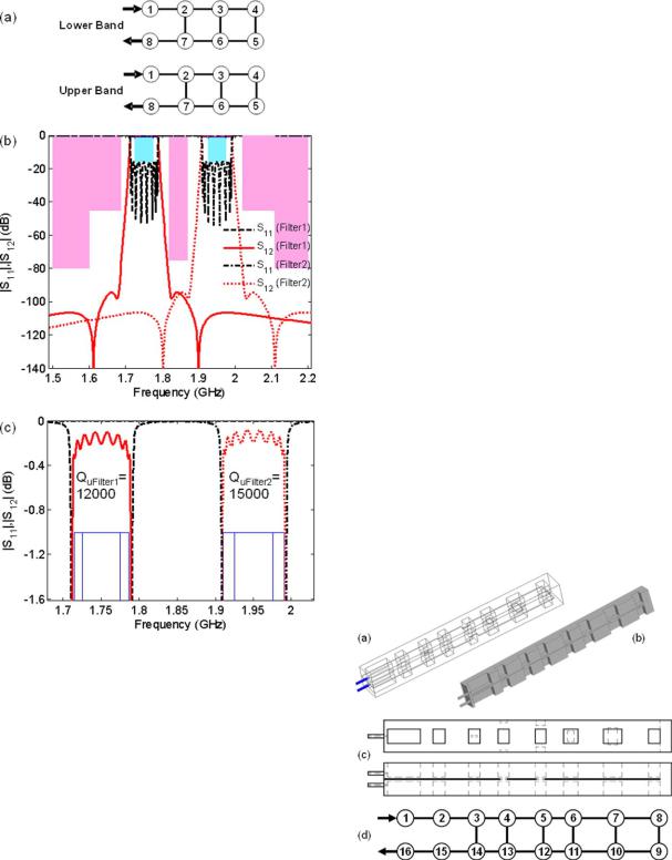
The 8–4 filter will satisfy the rejection requirements, but requires a higher Qu value to match the performance of the dual-band realization (Fig. 3c). Thus, a clear benefit of the dual-band cross-coupled resonator approach is that we can reduce the unloaded Q of the resonators to a moderate Qu 54000 with more margin at the extreme of the passbands (see Fig. 2c) than using single-band filters. This Qu 54000 can be achieved with air-filled metallic ridge waveguide resonators. The realization and design steps will be detailed in the next section.
III. REALIZATION IN RIDGE WAVEGUIDE
Since the achievable insertion loss even with a Qu of 4000 can meet the requirements in the nominal band, we decided to use a 16–10 dual-band filter rather than 14–10 to provide a wider margin on the rejection. The dual-band cross-coupler resonator filter will follow an E-plane-like realization (similar to the arrangement when rectangular waveguides are placed ones over the others) [17]. Figure 4 shows the proposed realization for this configuration, where the resonators of the filter will be realized using sections of propagating ridge waveguide arranged in a top-bottom configuration allowing longitudinal couplings between resonators of the same row and cross-couplings between resonators in different rows. The basic details of this configuration will be briefly commented now for the sake of the clarity.
The well-known longitudinal couplings in ridge waveguide filters are realized using sections of evanescent
Figure 3 (a) Schematic diagram of two independent singleband 8–4 filters; (b) Ideal circuit response of the Filters 1 and 2;
(c) Detail of the insertion loss for Filters 1 and 2 with Qu of 12,000 and 15,000, respectively.
two single-band filters each of order 8–4 (eight poles with four transmission zeros, also in canonical configuration) are used to realize the required responses. This dual-band approach is also compact and modular, since it avoids the splitter/combiner circuits on input and output required when using single-band filters. Such circuits are challenging to design for wide-band applications and will definitely add more losses to the unit.
The response of each filter is shown in Figure 3b, with the detail of the insertion loss in Figure 3c. It can be seen from Figure 3c that high unloaded quality factors of the resonant modes must be employed to get a performance at the edges of the passband that is comparable to the performance achieved by the presented dual-band approach.
Figure 4 Proposed filter realization: (a) full view of the 16–10 ridge waveguide filter (16 poles and 10 transmission zeros), with SMA input/output tapped into the first/last resonator; (b) structure split at the symmetry plane; (c) top and side views of the full filter, showing the ridge resonators at the top-bottom rows; (d) coupling scheme.
International Journal of RF and Microwave Computer-Aided Engineering/Vol. 00, No. 00, Month 2016
High-Selectivity Dual-Band Filters |
5 |
Figure 5 Structure to realize the electric coupling (a–c): (a) side view; (b) top view. Structure to realize the magnetic coupling (d–f): (d) side view; (e) top view. (c, f) Non-canonical waveguide cross-sections used to model the structure in mode matching (note the twofold symmetry).
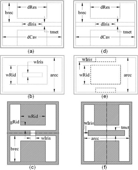
rectangular waveguides having the same outer dimensions as the ridge waveguide sections. Basically, the distance between the ridge resonators controls the coupling. Owing to the fact that the electric fields in the resonating section are mainly concentrated beneath the ridge sections, the cross-coupling is easily achieved by opening an iris in the intermediate wall between them. This coupling structure is detailed in Figure 5. The iris in Figures 5a–5c will be centered directly below the bottom of the ridge waveguide resonator in the cases where the required coupling is electric in nature (negative coupling). The iris in Figures 5d– 5f will be at the sides of the ridge waveguide sections adjacent to the outer walls in the cases where the required coupling is magnetic in nature (positive coupling).
The bottle neck in the proposed design is the achievable cross-couplings. The range of cross-couplings that can
be synthesized relates directly to the achievable bandwidths of the filters. Figure 6 shows the coupling values obtained for the irises realizing the cross-couplings. With a fractional bandwidth of approximately 15%, the required values for the couplings are challenging, but feasible as shown in Figure 6.
A study of the unloaded quality factor Qu of the chosen resonator using different materials was performed. The results are summarized in Table II. It shows that with un-plated metallic realization adequate values can be achieved to fulfill the specifications in Table I, as long as the dual-band approach is used to exploit the wideband nature of the 15% cross-coupled filter.
The proposed filter can be analyzed using the MM [17, 19], which has three main steps. First, the filter is segmented into a number of uniform waveguides along
International Journal of RF and Microwave Computer-Aided Engineering DOI 10.1002/mmce

6 Fahmi, Ruiz-Cruz, and Mansour
Figure 6 Actual coupling and loaded resonant frequency for the structures in Figure 5, varying the main parameters of the irises: (a) electric coupling by centered iris as in Figures 5a–5c; (b) magnetic coupling by side iris as in Figures 5d–5f. Other dimensions are found in Table II.
the longitudinal direction, taking into account the symmetries of perfect electric and magnetic wall of the problem. Our filter is made up of rectangular and ridge waveguides with noncanonical cross-sections, as shown in Figure 5.
Second, the generalized scattering matrix of the step between two consecutive nonequal waveguides is calculated. Finally, in a third step, cascading of the generalized scattering matrices of the individual steps provides the
TABLE II Air-Filled Ridge Waveguide Resonator
Resonant Frequency |
|
1.9 GHz (First Spurious at 7.3GHz) |
Ridge metal: (as in Fig. 5) |
width wRid 5675 mil, air gap gRid 575 mil, length dRes 5518 mil |
|
Enclosure cavity: (as in Fig. 5) |
|
arec 51500 mil, |
|
|
brec 5750mil, dCav 51823 mil |
Material |
Conductivity r [S/m] |
Unloaded Quality Factor Qu |
|
|
|
|
6 |
|
Silver |
61 106 |
4550 |
Copper |
58 106 |
4400 |
Aluminum |
38 10 |
3600 |
International Journal of RF and Microwave Computer-Aided Engineering/Vol. 00, No. 00, Month 2016

High-Selectivity Dual-Band Filters |
7 |
Figure 7 Optimized MM response of the dual-band 16–10 ridge waveguide filter: (a) comparison with the ideal circuit response (Cir); (b) comparison with the HFSS response.
filter response. To have an accurate response, enough modes have to be used in the computations [19]. For instance, in the filter that is simulated in the next section,
Figure 8 Proposed mechanical assembly of the ridge waveguide realization of the filter: two identical parts with a lid inbetween. Box dimensions in inches.
Figure 9 (a) Photograph of the assembled fabricated filter; (b) measured in-band response of the fabricated filter; (c) detail of the insertion loss.
all the modes with cutoff frequency lower than 120 GHz (around 250 modes in the ridge waveguides) were used in the final accurate computations of the filter response before manufacturing.
The MM method can be used to obtain the full-wave response of the filter, but it can also be applied to the input/output resonator, or just to two coupled resonators. The actual coupling values of the waveguide implementation can be extracted from these simpler problems [11, 12], to get initial dimensions for the filter. The input/ output coupling is realized using an SMA coaxial attached to a ridge waveguide resonator. The actual coupling between two resonators is obtained by combining the resonant frequencies of two equal coupled ridge cavities.
International Journal of RF and Microwave Computer-Aided Engineering DOI 10.1002/mmce

8 Fahmi, Ruiz-Cruz, and Mansour
TABLE III Dimensions of the Filter in Figure 11
Cross-Sectional Dimensions in Mils (as Fig. 5) |
|
||||
arec |
1248.2 |
brec |
373.5 |
wRid |
624.1 |
gRid |
18.67 |
wIrisb/c |
599.1 |
tmet |
2.5 |
Longitudinal Dimensions in Mils |
|
|
|||
dK1 |
245.3 |
dK2 |
183.7 |
dK3 |
722.1 |
dK4 |
784.4 |
dRa |
616.8 |
dRb |
836.7 |
dRc |
1050.1 |
dIrisb |
83.3 |
dIrisc |
716.4 |
|
|
|
|
|
|
computation time and computer memory resources were needed to simulate this high-order filter using the HFSS software, not practical for accurate full-wave optimization.
Proposed mechanical realization of the filter is shown in Figure 8. The whole length of the filter (with enclosure) is 14 in. The lid between the two identical parts has
Figure 10 Comparison of the experimental results of the fabricated filter with MM. (a) In-band response; (b) wide-band response.
IV. DESIGNS AND EXPERIMENTAL RESULTS
A. 16–10 Dual-Band Filter with 15.4% Fractional Bandwidth
The 16–10 dual-band filter has been designed, fabricated, and tested. An ideal circuit for the 16–10 filter was first obtained (see Fig. 7a). Based on the ideal circuit parameters, initial dimensions of the waveguide realization were generated using coupling curves such as those in Figure 6. However, these coupling curves only take into account the coupling of two single resonators and, thus, the loading effect of nonadjacent resonators must be taken into account [11].
The filter was modeled using rigorous MM. Given the complexity of the filter in terms of its high order and its topology, MM presents the most suitable numeric method to optimize the filter structure [11]. The optimized response obtained by mode-matching simulation is shown in Figure 7a, compared with the ideal circuit response driving the optimization. Additional analysis is presented in Figure 7b using the commercially available software HFSS which is based on a different numeric method (finite element method). The good agreement between the responses validates the design for fabrication and testing. It should, however, be mentioned that a significant
Figure 11 (a) Cross-sectional side view of the E-plane filter topology with two electric coupling center irises. (b) Full-wave response of the filter by MM and HFSS. (c) Detail of the insertion loss simulated with HFSS assuming copper metallic conductors.
International Journal of RF and Microwave Computer-Aided Engineering/Vol. 00, No. 00, Month 2016
|
|
|
High-Selectivity Dual-Band Filters |
9 |
|
TABLE IV Summary of Reported Canonical Filter Ridge Waveguide Designs |
|
|
|||
|
|
|
|
|
|
|
|
|
|
Number of Poles- |
|
Reference |
E/H-Plane Configur. |
Single/Dual |
Fractional Bandwidth |
Transm. Zeros |
|
|
|
|
|
|
|
16 |
H-plane |
Dual |
59% |
6–2 |
|
17 |
E-plane |
Single |
5% |
4–2 |
|
18 |
LTCC E-plane |
Single |
11% |
6–2 |
|
This work IV.A |
E-plane |
Dual |
15% |
16–10 |
|
This work IV.B |
E-plane |
Dual |
37% |
6–2 |
|
|
|
|
|
|
|
a thickness of 0.049 in that allows an easy construction of the irises for the cross-couplings. Provisions for post manufacture tuning of the resonant frequencies of the resonators were included in the mechanical design to have a means to offset the machining tolerance.
The filter was fabricated by milling of aluminum in three parts: two top-bottom identical parts and the lid with the cross-coupling irises in the middle. The parts were assembled and the filter was tested. Figure 9 shows a photograph of the fabricated prototype as well as the measured in-band response of the dual-band filter. It is worth noting that despite the fact that the filter was machined of Aluminum without any plating, the insertion loss of the filter is quite good meeting the 1 dB limit in the specifications. Improved insertion loss which can meet even more stringent requirements is quite possible using high quality silver plating and keeping the dual-band approach.
Figure 10 shows the measured response compared to full-wave MM. There is a good agreement, although there is a small frequency shift between both simulated and measured response from the fabricated prototype. The mode-matching response also accurately predicts the exact location of the spurious passbands which start to appear at 7 GHz, as it can be seen if Figure 10b. This spurious-free response is also another clear advantage of the proposed realization, which allows avoiding low-pass cleaning filters, further reducing the overall insertion loss.
B. Application to Filters with Very Wide Bandwidth
To further validate the potential of this approach to get wideband filters, a second dual-band filter has been designed for the same center frequency of 1.8 GHz as the previous realization, but with a wider separation between sub-bands. The dimensions of this filter are given in Table III, with the layout in Figure 11a, and full-wave response in Figures 11b and 11c. Both MM response and HFSS response are very similar. The MM response included approximately 200 modes in the ridge waveguide, with symmetry of perfect magnetic wall in the longitudinal symmetry plane.
This design has a 37% fractional bandwidth. As shown in the summary of different works in Table IV, the designs in Sections IV.A and IV.B introduce practical designs in E-plane configuration for wide bandwidths dual-band responses. The design in Figure 11 has its first passband centered at 1.57 GHz with 62 MHz bandwidth, while the second passband is centered at 2.22 GHz with62 MHz bandwidth. The two bands have maximum
in-band return loss of 20 dB and a guard band of 410 MHz with better than 30 dB of attenuation centered at 1.8 GHz.
V. CONCLUSIONS
A very compact realization of canonical folded ridge waveguide dual-band filter was presented in E-plane-like configuration using ridge waveguide resonators coupled by sections of rectangular waveguide and irises in the intermediate wall. A summary of the works using this type of canonical configuration is found in Table IV. This work has introduced the potential of the E-plane configuration for wide bandwidth and dual-band responses not reported before, using a large order filter of 16 poles with 10 transmission zeros, which is a very remarkable aspect from the engineering and experimental point of view.
Moreover, this article has been focused on using this potential within the context of actual practical applications where dual-band filter provides an added advantage of improved insertion loss performance, with un-plated ridgewaveguides, compactness, and modularity. This is due to the very wide-band nature of the filter in comparison with a single-band filter approach, allowing more margins at the band edges where roll-off is usually detrimental and also avoiding additional splitter/combiner networks with their added losses and complexity. The guard band between the two passbands is achieved by locating an appropriate number of transmission zeros within the band, thus providing the required rejection characteristics, while maintaining the advantages of wide-band filters for insertion loss.
A very challenging high-order prototype filter, similar to those required by typical wireless communications transceivers, was built and measured to verify the design approach. The measured response of the 16–10 filter almost met very stringent specification requirements.
ACKNOWLEDGMENT
This work was supported in part by the Ontario Ministry of Research and Innovation, ON, Canada, and COM DEV Ltd. Cambridge, ON, Canada, and by the Spanish Government under Project TEC2013-47106-C3-1/2-R (TECOAMP) and Comunidad de Madrid Project S2013/ ICE-3000 (SPADERADAR-CM).
REFERENCES
1.S. Holme, Multiple passband filters for satellite applications, Proc 20th AIAA Int Commun Satellite Syst Conf Exhibit, 2002, Montreal, Quebec, Canada, paper no. AIAA-2002-1993.
International Journal of RF and Microwave Computer-Aided Engineering DOI 10.1002/mmce
10 Fahmi, Ruiz-Cruz, and Mansour
2.R.R. Mansour, Filter technologies for wireless base stations, IEEE Microw Mag 5 (2004), 68–74.
3.G. Macchiarella and S. Tamiazzo, Dual-band filters for base station multi-band combiners, 2007 IEEE MTT-S Int Microw Symp Dig, June 2007, Honolulu, HI, USA, pp. 1289–1292.
4.R. Zhang and R.R. Mansour, Dual-band dielectric-resonator filters, IEEE Trans Microw Theory Tech 57 (2009), 1760– 1766.
5.G. Machiarella and S. Tamiazzo, Design techniques for dualpassband filters, IEEE Trans Microw Theory Tech 53 (2005), 3265–3271.
6.J.A. Ruiz-Cruz, M. Fahmi, and R.R. Mansour, Triple-conduc- tor combline resonators for dual-band filters with enhanced guard-band selectivity, IEEE Trans Microw Theory Tech 60 (2012), 3969–3979.
7.S. Bila, R.J. Cameron, P. Lenoir, V. Lunot, and D. Seyfert, Chebyshev synthesis for multi-band microwave filters, 2006 IEEE MTT-S Int Microw Symp Dig, June 2006, San Francisco, CA, USA, pp. 1221–1224.
8.M. Mokhtari, J. Bornemann, K. Rambabu, and S. Amari, Coupling-matrix design of dual and triple passband filters, IEEE Trans Microw Theory Tech 54 (2006), 3940–3946.
9.V. Lunot, S. Bila, and D. Seyfert, Optimal synthesis for multi-band microwave filters, 2007 IEEE MTT-S Int Microw Symp Dig, June 2007, Honolulu, HI, USA, pp. 115–118.
10.Y. Zhang, K.A. Zaki, J.A. Ruiz-Cruz, and A.E. Atia, Analytical synthesis of generalized multi-band microwave filters, 2007 IEEE MTT-S Int Microw Symp Dig, June 2007, pp. 1273–1276.
11.R.J. Cameron, R.R. Mansour, and C. Kudsia, Microwave filters for communication systems: Fundamentals, design and applications, Wiley, New York, 2007.
12.Y. Zhang, J.A. Ruiz-Cruz, and K.A. Zaki, Inline and canonical stripline filters with ridge coupling sections for LTCC applications, Int J RF Microw CAE 19 (2009), 354–363.
13.B. Chen, T. Shen, and R. Wu, Design of tri-band filters with improved band allocation, IEEE Trans Microw Theory Tech 57 (2009), 1790–1797.
14.M. Memarian and R.R. Mansour, Dual-band half-cut dielectric-resonator filters, 2009 Eur Microw Conf, September 2009, Rome, Italy, pp. 555–558.
15.S. Amari and M. Bekheit, A new class of dual-mode dualband waveguide filters, IEEE Trans Microw Theory Tech 56 (2008), 1938–1944.
16.M. Fahmi, J.A. Ruiz-Cruz, R.R. Mansour, and K.A. Zaki, Compact wide-band ridge waveguide dual-band filters, 2010 IEEE MTT-S Int Microw Symp Dig, May 2010, Anaheim, CA, USA, pp. 888–891.
17.J.A. Ruiz-Cruz, M.A. El Sabbagh, K.A. Zaki, J.M. Rebollar, and Y. Zhang, Canonical ridge waveguide filters in LTCC or metallic resonators, IEEE Trans Microw Theory Tech 53 (2005), 174–182.
18.M.M. Fahmi, J.A. Ruiz-Cruz, K.A. Zaki, and A.J. Piloto, LTCC wide-band canonical ridge waveguide filters, 2005 IEEE MTT-S Int Microw Symp Dig, June 2005, Long Beach, CA, USA, pp. 249–252.
19.G. Conciauro, M. Guglielmi, and R. Sorrentino, Advanced modal analysis: CAD techniques for waveguide components and filters, Wiley, New York, 1999.
BIOGRAPHIES
Mohamed M. Fahmi (S’05–M’09) received B.Sc. (with Honors) in Electronics Engineering from Mansoura University, Egypt in 1999. From 1999-2000 he worked as a Teaching/Research Assistant in the Department of Electronics Engineering at Mansoura University. From 2001-2003 he worked as a Research Assistant at Howard University, Washing-
ton DC, USA where he received his MS degree in May 2003. From 2003-2007 he worked as a Teaching/Research Assistant at the University of Maryland, College Park, USA where he received his PhD in December 2007. He worked as a post doctoral researcher at the University of Maryland in 2008. From September 2008 to January 2012 he worked at the Department of Electrical and Computer Engineering at the University of Waterloo as a post-doctoral fellow. In February 2012 he joined Nanowave Technologies Inc., Etobicoke, ON, Canada as a microwave Engineer. His current research interests include CAD of microwave devices.
Jorge A. Ruiz-Cruz received the Ingeniero de Telecomunicacion degree in 1999 and the PhD degree in 2005, both from the Universidad Politecnica de Madrid (UPM), Spain. Since 2006, he has been with the Universidad Autonoma de Madrid, Madrid, Spain, where in 2009 he became an Associate Professor. His current research interests are the Computer-
Aided Design of microwave passive devices and circuits (filters, multiplexers, ortho-modes, etc.).
Raafat R. Mansour (S’84-M’86-SM’90- F’01) was born in Cairo, Egypt, on March 31, 1955. He received the B.Sc (with honors) and M.Sc degrees from Ain Shams University, Cairo, Egypt, in 1977 and 1981, respectively, and the Ph.D. degree from the University of Waterloo, Waterloo, ON, Canada, in 1986, all in electrical engineering. In 1981, he was a Research
Fellow with the Laboratoire d’Electromagnetisme, Institut National Polytechnique, Grenoble, France. From 1983 to 1986 he was a Research and Teaching Assistant with the Department of Electrical Engineering, University of Waterloo. In 1986, he joined COM DEV Ltd., Cambridge, ON, Canada, where he held several technical and management positions with the Corporate Research and Development Department. In 1998, he received the title of a Scientist. In January 2000, he joined the University of Waterloo, as a Professor with the Electrical and Computer Engineering Department.
International Journal of RF and Microwave Computer-Aided Engineering/Vol. 00, No. 00, Month 2016