

диафрагмированные волноводные фильтры / a57de7e8-1235-4f1a-b6e7-97c88428d133
.pdfReceived: 1 October 2018
DOI: 10.1002/mop.31741
R E S E A R C H A R T I C L E
Topology optimization and experimental verification of compact E-plane waveguide filters
Daniel Gert Nielsen1 |
| |
|
Søren Damgaard Pedersen2 | |
||
Vitaliy Zhurbenko1 |
| |
|
Villads Egede Johansen3 |
| |
|
Ole Sigmund2 |
| Niels Aage2,4 |
|
1Department of Electrical Engineering, Technical University of Denmark, Kgs. Lyngby, Denmark
2Department of Mechanical Engineering, Technical University of Denmark, Kgs. Lyngby, Denmark
3Department of Chemistry, University of Cambridge, Cambridge, United
Kingdom
4Centre for Acoustic-Mechanical Micro Systems (CAMM), Technical University of Denmark, Kgs. Lyngby, Denmark
Correspondence
Daniel Gert Nielsen, Department of Electrical Engineering, Technical University of Denmark, Kongens Lyngby 2800, Denmark.
Email: dgniel@elektro.dtu.dk
Abstract
This article presents a numerical method to design compact E-plane waveguide filters. The key feature of the proposed method is that the conducting layout of the filters is automatically determined based on a desired filter characteristic. This extreme level of design freedom is obtained using the numerical optimization technique called topology optimization. The filters are complex in shape but easy to mass-produce with low-cost conventional methods. The method is verified experimentally by measurement of responses similar to the numerical predictions.
K E Y W O R D S
compact filters, E-plane filters, rectangular waveguide, topology
optimization
1 | INTRODUCTION
Waveguide filters are indispensable assets in high frequency systems such as radars and satellites.1 Several types of waveguide filters exist where E-plane filters have been widely used in millimeter wave applications since their introduction by Konishi and Uenakada,2 due to their compact size, lowcost, mass produceability, and low loss.
Rising demands to performance, frequency selectivity, size and weight of waveguide filters mean that they are constantly being improved. Metallic insert filters are subject to such improvements. One method is to place transmission zeroes at discrete frequencies.3,4 Goussetis et al.5 also utilize this method and a compact filter is obtained by cross coupling of resonators. This filter is 35 mm long, corresponding to 1.05λg, where λg is the wavelength of the center frequency in the passband in a rectangular waveguide. All of the above mentioned filters are based on short-circuiting the waveguide walls. LopezVillarroya et al.6 presents a waveguide filter with c-shaped resonators which are decoupled from the waveguide walls.
Though E-plane filters have several advantages in terms of easy manufacturing, The European Space Agency (ESA) has recently produced cavity filters with extremely high design freedom enabled by metallic 3D printing of the entire waveguide including the waveguide filter.7 It would therefore be desirable to have a design method with geometric freedom similar to that of ESA’s cavity filters, but maintaining the low costs of conventional E-plane filters.
Computer-based optimization of waveguide bandpass filters is an established research topic. Bornemann et al.8 present an evolution based optimization strategy for ladder-like filter structures. Aydogan et al.9 optimize the placement and thickness of dielectric slabs placed in a waveguide with a Levenberg-Marquadt optimization scheme. Budimir and Goussetis10 optimize asymmetrical ridged-waveguide bandpass filters with respect to the Chebyvev criterion, where the height of the ridges are the variables. Ouedraogo et al.11 present pixelated filter inserts for bandstop waveguide filters, optimized with a genetic algorithm.
Gradient-based topology optimization (TO) has proven to be use-full for optimizing aerospace applications such as wings,12 structural, dynamic, and fluid mechanics13 and for various types of electromagnetic problems. For conductor based material distribution problems in electromagnetics, most effort has been put in the design of different types of antennas, see for example, 14–16 Diaz and Sigmund17 propose a method for designing metamaterials with negative permeability. Hassan
Microw Opt Technol Lett. 2019;1–8. |
wileyonlinelibrary.com/journal/mop |
© 2019 Wiley Periodicals, Inc. |
|
1 |
|

2 |
|
|
NIELSEN ET AL. |
|
|
||
|
|
|
|
et al.18 maximize the matching between a coaxial cable and rectangular waveguide. Khalil et al.19 optimize the shape of dielectric microwave components for dual-mode waveguide filters. Recently, gradient based TO has been demonstrated for the optimization of bandpass filters.20
The procedure proposed in Reference 20 is extended here, applied to practical problems and verified experimentally. The designs are etched on printed circuit boards (PCBs). The design method empowers complete design freedom and thereby the ability to tailor the filters to distinct frequencies ranges, thus the proposed method can be utilized to create various filter types, such as bandpass, bandstop, highpass filters, or filters with several operating bands.
The remainder of the article is organized as follows; first, we present the filter design methodology along with the governing physical model. Then a description of the fabrication process and the experimental setup is given. Finally, we present a number of optimized filters and discuss the achieved characteristics.
2 | DESIGN THEORY
This section serves as a brief overview of the overall design method. The main goal in Reference 20 was to devise a design methodology capable of realizing optimized filter inserts with specified filter characteristics. A key point was that the design should be obtained with no a priori knowledge of the layout of the filter insert itself. That is, the optimization starts with a clean PCB slab in a waveguide, and then automatically determines the spatial layout of the conducting material which results in the desired filter characteristics. This unusual degree of design freedom is achieved using the numerical optimization technique called TO. TO is an iterative numerical method used to determine optimized material distributions in a multitude of different physical disciplines such as structural engineering, optics, acoustics, and fluid dynamics to name but a few.13
The TO method in Reference 20 is most easily described using an example of a bandpass filter characteristics shown in Figure 1. Using a variable number of discrete target frequencies; here a total of nine, marked with crosses and circles; the aim of the optimization is to maximize the transmission in the passband (upward arrows) while minimizing the out-of-band transmission (downward arrows).
This characteristic can be obtained by the formulation of a general max-min optimization problem, which also serves as an objective function used to evaluate the performance of the filter
Φ = max |
min minj f |
|
S21 |
ωj |
|
, minj z |
1− S21 |
ωj |
, |
|||
|
2I |
|
|
2I |
|
|
|
|
|
|||
|
|
|
|
|
|
|
|
|
|
|
|
|
where If |
and Iz correspond to |
full and |
zero |
transmission |
||||||||
(crosses and circles in Figure 1), respectively, and Φ = 1 corresponds to the situation where all the scattering parameters of all the discrete frequencies have reached the optimum. The situation Φ = 0 is present when one or more of
|S | [dB] 21
Frequency
FIGURE 1 Schematic illustration of the optimization of a bandpass filter at discrete frequencies (phase 2). The upward arrows on the targeted frequencies indicate that these are to be maximized and the downward arrows indicate the targeted frequencies to be minimized
the scattering parameters act entirely opposite of the intended.
However, the findings in Reference 20 show that obtaining functional filter designs with sharp rejection skirts is a challenging optimization problem. Therefore the authors propose a two phase optimization scheme which results in a more robust design methodology. The idea is to first design a series of structures with full transmittance within the operating band of the final filter as seen in Figure 2. The phase 1 design problem is illustrated in Figure 4 (top), which shows that three separate structures with maximum transmittance are to be determined, that is, each structure corresponds to one target frequency to be maximized as shown in Figure 1. The series of structures can be chosen arbitrarily, but one should keep in mind that the PCB slab must have enough space to contain a number of nonoverlapping design domains. A rule of thumb is to include at least two frequencies (and domains) such that the upper and lower limit of the bandpass region are included.
Having completed the design of three structures with full transmittance in a finite frequency range the next phase is to design the actual filter characteristics. That is, combining these structures into a single PCB slab, see Figure 3. We allow the optimizer to simultaneous maximize and minimize the relevant discrete frequencies as seen on Figure 1, note
|S | [dB] 21
Frequency
FIGURE 2 Schematic illustration of the optimization of three structures that have full transmission in a finite frequency range (phase 1)

NIELSEN ET AL. |
|
3 |
|
|
|
||
|
|
|
|
FIGURE 3 Schematic illustration of the transition from a PCB slab subdivided into a number of independent optimization problems to obtain phase 1 results. These results are collected into a single domain as the initial guess for the phase 2 optimization problem. The bottom illustration is the results of the phase
2 optimization, which is the final filter design [Color figure can be viewed at wileyonlinelibrary.com]
that the target frequencies to be maximized in phase 2 are the same as phase 1 .
The complete design approach can be summarized as follows:
1.Optimize a number of structures with full transmittance separated in both space and frequency. No initial design is needed c.f. Figure 3 (top).
2.Combine these structures into a single PCB slab and use this as an initial guess for the actual filter characteristic optimization, c.f. Figure 3 (bottom).
The solution to the optimization problem is obtained by the design problem cast as two smooth mathematical programs, which can be solved efficiently with gradient based methods. In all of the presented results we use the method of moving asymptotes.21,22
2.1 | The waveguide model
contact has a big influence on the performance of the filter. Thus, to enhance the practical applicability of the proposed design methodology, we add a small clearance (hf in Figure 4) between conductor and waveguide walls.
Throughout this work we use a waveguide model as shown in Figure 4. For the phase 1 optimization the design domain is split into three subdomains (Ω1, Ω2, and Ω3) which are collected into a single domain (Ω) for phase 2, compare with Figures 3 and 4. The operating range for the filters in this work is 8.0 to 12.0 GHz, corresponding to the rectangular waveguide standard WR-90. The filters are compact with a length of 32.6 mm corresponding to 1.1λg when the center frequency is 10.3 GHz.
2.2 | Numerical setup
The waveguide model consists of a two-port system, as shown in Figure 4 with a TE10 wave incident from the left. To obtain the numerical prediction of the waveguide with the filter inserted we solve Maxwell’s equation cast in the frequency domain, that is, .
r |
|
|
r |
r |
|
− 0 ϵr − |
|
ωϵ0 |
|
Ω |
|
|
× |
|
μ−1 |
|
× E |
k2 |
j |
σðxÞ |
E = 0 in |
|
, |
|
|
|
|
|
where μr is the relative permeability, ϵr is the relative permittivity, σ(x) is the spatially varying conductivity, ω is the frequency of the microwave signals, E is the electric field,
k = ωpϵ μ is the free space wavenumber, ϵ and μ are the
0 0 0 0 0
permittivity and permeability of vacuum, respectively. We note that the spatial variation in conductivity is introduced as a design variable for the optimization. That is, the task of the optimization process is to determine where to place conductive material and where not to. For details on the optimization method the reader is referred to References 20,23.
The waveguide walls are modeled as perfect electric conductors
n × E = 0 on ΓPEC,
Before presenting the model waveguide problem and the Maxwell solver, we note that the design problem solved in this work has one major difference to.20 In this work the filter insert is prohibited from touching the waveguide walls. This is done to make the fabrication process more robust, since it is often not easy to provide a good contact between the waveguide and the metal of the insert. The quality of this
FIGURE 4 Design domains of phase 1 (top) and phase 2 (bottom). Dimensions are a = 22.86 mm, b = 10.16 mm, L0 = 5.00 mm, Lf = 32.59 mm, hf = 0.50 mm, dr = 1 mm,
tc = 0.035 mm, and ts = 0.79 mm. The filter insert is a Rogers duroid 6002 and the operating frequency range is between 8.0 and 12.0 GHz [Color figure can be viewed at wileyonlinelibrary.com]

4 |
|
|
NIELSEN ET AL. |
|
|
||
|
|
|
|
where n is an outward normal vector to the respective surfaces. The port conditions are introduced using the waveguide port boundary conditions.24 In the operating range of the filter, only the TE10 mode exists and therefore the boundary condition is as follows
eTE x = |
2 |
8 sin πx=a |
9: |
|||
|
|
−r |
|
|
0 |
Þ= |
10 |
ð Þ |
|
ð |
|
||
|
ab< |
0 |
||||
|
|
|
: |
|
; |
|
The incident field Einc is applied at port Γ1, which gives rise to the following boundary conditions
ð
n × r × E = jγe10TE Γ1 e10TE EdΓ −2jγe10TE on Γ1,
ð
n × r × E = jγe10TE Γ2 e10TE EdΓ on Γ2,
q
where γ = kz2 −k02 defines the propagation constant, kz =
π/a is the wave cutoff number, and we note that only port 1 is subject to the incident field.
The boundary-value problem is solved by the finite element method using curl-conforming elements.24 The geometries are generated and discretized using CUBIT25 and
subsequently partitioned by METIS.26 The indefinite system of equations is then solved using MUMPS27,28 using an in-
house parallel code framework written in C++ using MPI.22 The in-house code is validated using the commercial software Comsol Multiphysics 5.3. The two models are coherent when modeling a waveguide with an inserted filter.
3 | NUMERICAL AND
EXPERIMENTAL RESULTS
The filters are manufactured by photolithography on Rogers Duroid 6002 PCB with ϵr = 2.94 and a thickness of 0.76 mm, which ensures that the filter is mechanically stable. Figure 5 shows a filter design with a 5 euro cent for scale. The manufacturing tolerances are estimated to be around 0.2 mm.
The performance of the optimized filters were tested experimentally on a vector network analyzer. We fabricated a 50 mm long WR-90 rectangular waveguide in copper with an insertion slot to slide in the PCBs without disassembling the waveguide (Figure 5).
3.1 | Physical verification of numerical model
Several experiments showed a discrepancy from the numerical results, where the experimental results were frequency up-shifted 0.3-0.5 GHz. To account for this, the permittivity of the PCB substrate from the data sheet (ϵr = 2.94) was corrected, such that the numerical and experimental results better correlate. It was found that changing ϵr = 2.45 in the numerical model provides a good fit in all cases. We have
FIGURE 5 Two-piece copper waveguide used in the experimental work and a filter design with a 5 euro cent for scale [Color figure can be viewed at wileyonlinelibrary.com]
investigated this issue further by manufacturing over and under etched designs, numerically we investigated mesh dependency, thickness of the conducting layout and over/under etching. We found that these parameters influence the scattering parameters, however, not as significantly as the observed up-shift of 0.3-0.5 GHz.
3.2 | Bandpass filter
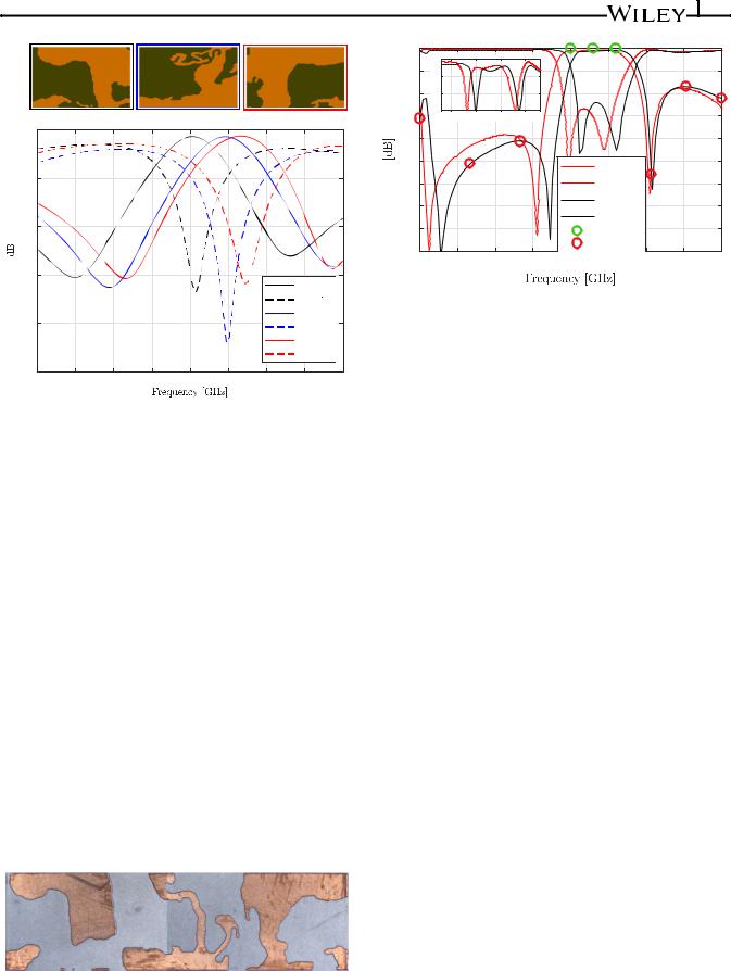
Here we will elaborate on how a bandpass filter is designed with the proposed method and the performance of this will be evaluated. The three structures with full transmittance in a finite frequency range from the phase 1 optimization were tailored to serve as starting guess for the phase 2 optimization of a bandpass filter with center frequency of 10.3 GHz. The designs and performances of the three structures are shown in Figure 6. At the start of phase 2 the initial guess from phase 1 is “smeared out,” in-order to increase the design freedom and to avoid being stuck in a local minimum. The phase 2 optimization is implemented such that it maximizes transmission for the three distinct frequencies that were also maximized in phase 1. The six frequencies to be minimized are evenly distributed in the stopband. The manufactured final PCB design is shown in Figure 7.
NIELSEN ET AL. |
|
|
|
|
|
|
|
|
|
|
|
|
|
|
|
|
|
5 |
||
|
|
|
|
|
|
|
|
|
|
0 |
|
|
|
|
|
|
|
|
|
|
|
|
|
|
|
|
|
|
|
|
|
0 |
|
|
|
|
|
|
|
|
|
|
|
|
|
|
|
|
|
|
|
-5 |
-1 |
|
|
|
|
|
|
|
|
|
|
|
|
|
|
|
|
|
|
|
|
|
|
|
|
|
|
|
|
||
|
|
|
|
|
|
|
|
|
-10 |
-2 |
|
|
|
|
|
|
|
|
||
|
Struc1 |
|
Struc2 |
|
|
Struc3 |
|
-15 |
-3 |
|
|
|
|
|
|
|
|
|||
0 |
|
|
|
|
9.5 |
10 |
10.5 |
11 |
|
|
|
|
|
|||||||
|
|
|
|
|
|
|
|
-20 |
|
|
|
|
|
|
|
|
|
|||
|
|
|
|
|
|
|
|
|
|
|
|
|
|
|
|
|
|
|||
|
|
|
|
|
|
|
|
|
-25 |
|
|
|
|
|
|S21| Mea. |
|
|
|||
-5 |
|
|
|
|
|
|
|
|
|
|
|
|
|
|
|
|
|
|||
|
|
|
|
|
|
|
|
-30 |
|
|
|
|
|
|S11| Mea. |
|
|
||||
|
|
|
|
|
|
|
|
|
|
|
|
|
|
|
|
|||||
|
|
|
|
|
|
|
|
|
-35 |
|
|
|
|
|
|S21| Num. |
|
|
|||
-10 |
|
|
|
|
|
|
|
|
-40 |
|
|
|
|
|
|S11| Num. |
|
|
|||
|
|
|
|
|
|
|
|
|
|
|
|
|
Max |
|
|
|
||||
|
|
|
|
|
|
|
|
|
-45 |
|
|
|
|
|
Min |
|
|
|
||
|
|
|
|
|
|
|
|
|
|
|
|
|
|
|
|
|
|
|||
|
|
|
|
|
|
|
|
|
|
8 |
8.5 |
|
9 |
9.5 |
10 |
10.5 |
11 |
11.5 |
12 |
|
-15 |
|
|
|
|
|
|
|S21|Struc1 |
|
|
|
|
|
|
|
|
|
|
|
||
|
|
|
|
|
|
|
|
|
|
|
|
|
|
|
|
|
|
|||
|
|
|
|
|
|
|
|S11|Struc1 |
FIGURE 8 Comparison between numerical and experimental |
|
|||||||||||
|
|
|
|
|
|
|
|S21|Struc2 |
|
||||||||||||
-20 |
|
|
|
|
|
|
|S11|Struc2 |
results for the bandpass filter in Figure 7. Red curves are the |
|
|||||||||||
|
|
|
|
|
|
|
|S21|Struc3 |
measured results, and the black curves are the frequency response |
||||||||||||
|
|
|
|
|
|
|
|S11|Struc3 |
from the numerical model. The circles indicate the discrete |
|
|||||||||||
-25 |
|
|
|
|
|
|
|
|
|
|||||||||||
|
|
|
|
|
|
|
|
frequencies used in the optimization. Maximum measured IL in the |
||||||||||||
8 |
8.5 |
9 |
9.5 |
10 |
10.5 |
11 |
11.5 |
12 |
||||||||||||
|
|
|
|
|
|
|
|
|
bandpass region is 0.6 dB and minimum rejection outside of the |
|
||||||||||
FIGURE 6 S-parameters and shape of the structures originating |
passband is 8.8 dB [Color figure can be viewed at |
|
|
|||||||||||||||||
wileyonlinelibrary.com] |
|
|
|
|
|
|
||||||||||||||
from a phase 1 optimization. Orange areas are the copper features, |
|
|
|
|
|
|
||||||||||||||
|
|
|
|
|
|
|
|
|
|
|
||||||||||
in the dark green areas no conducting material is present [Color |
9.0 GHz, only the rightmost part of the filter is active. In the |
|||||||||||||||||||
figure can be viewed at wileyonlinelibrary.com] |
|
|
||||||||||||||||||
|
|
|
|
|
|
|
|
|
bandpass region (10.4 GHz) most of the filter is active. For the |
|||||||||||
Numerically obtained S-parameters for the bandpass filter |
roll-offs (9.8 GHz, 10.9 GHz) the field intensities have some |
|||||||||||||||||||
similarities we note that generally the rightmost part of the filter |
||||||||||||||||||||
are compared to measured S-parameters in Figure 8. The green |
||||||||||||||||||||
is more active at 10.9 GHz and the leftmost part at 9.8 GHz. |
||||||||||||||||||||
circles |
indicate the |
frequencies |
that |
were |
maximized |
during |
||||||||||||||
At 11.5 GHz, the field intensities take lower values, which is |
||||||||||||||||||||
optimization, and the red circles indicate the ones that were |
||||||||||||||||||||
also the case at 9.00 GHz, where we observe that the leftmost |
||||||||||||||||||||
minimized. Apart from a minor frequency shift, good agree- |
||||||||||||||||||||
part of the filter is not active. A general observation is that the |
||||||||||||||||||||
ment between the |
numerical and experimental |
results have |
||||||||||||||||||
electric field concentrates in the gap between the copper fea- |
||||||||||||||||||||
been obtained with a measured insertionloss (IL) of 0.6 dB and |
||||||||||||||||||||
tures and the waveguide walls. This is especially pronounced |
||||||||||||||||||||
a steep cut-of between the passband and the stopband. |
|
|||||||||||||||||||
|
for the roll-offs and the bandpass region. |
|
|
|
||||||||||||||||
The conducting layout seen in Figure 7 takes organic |
|
|
|
|||||||||||||||||
|
|
|
|
|
|
|
|
|
|
|
||||||||||
shapes, |
which is different from |
conventional E-plane |
filters, |
3.3 |
| |
Filter obtained with projection methods |
||||||||||||||
and it is as such difficult to comprehend how the filter works. |
||||||||||||||||||||
|
|
|
|
|
|
|
|
|
|
|
||||||||||
The design is therefore not easily obtainable through traditional |
At the cost of additional computational power, the filter |
|||||||||||||||||||
methods such as parameter optimization based on fixed geome- |
presented in Figure 8 can be improved with a numerical |
|||||||||||||||||||
tries. The time-average electric energy29 for five frequencies |
projection method based on the Heaviside function. The |
|||||||||||||||||||
located within and around the bandpass region are shown in |
method is thoroughly described in Reference 30. The |
|||||||||||||||||||
Figure 9. This serves to show that different parts of the filter |
phase 2 optimization is extended with the projection |
|||||||||||||||||||
are active depending |
on the |
frequency. |
For |
example, at |
method applied. Figure 10 shows minor, but distinct, |
|||||||||||||||
|
|
|
|
|
|
|
|
|
changes in shape and topology compared to Figure 7. |
|||||||||||
|
|
|
|
|
|
|
|
|
Figure 11 shows that the out-of-band performance is sig- |
|||||||||||
|
|
|
|
|
|
|
|
|
nificantly enhanced with a minimum measured rejection |
|||||||||||
|
|
|
|
|
|
|
|
|
of 16.0 dB, while the steep cut-off between the passband |
|||||||||||
|
|
|
|
|
|
|
|
|
and the stopband is maintained. The cost of this is a larger |
|||||||||||
|
|
|
|
|
|
|
|
|
IL of 1.5 dB for the manufactured design, whereas the |
|||||||||||
|
|
|
|
|
|
|
|
|
numerical model predicts an IL of 1.0 dB. Good correla- |
|||||||||||
FIGURE 7 Micrograph of the bandpass filter insert. The |
|
tion |
is |
obtained |
between |
the numerical |
model and |
the |
||||||||||||
|
manufactured |
design, |
especially |
in the |
bandpass region |
|||||||||||||||
difference in lighting is due to the merging of two images. Note |
||||||||||||||||||||
and the roll-offs. This extra step demonstrates that the |
||||||||||||||||||||
that the 0.5 mm blank substrate between the copper features and |
||||||||||||||||||||
the waveguide walls is not included here [Color figure can be |
design approach can be tweaked in different directions |
|||||||||||||||||||
viewed at wileyonlinelibrary.com] |
|
|
|
|
|
depending on criteria and purpose. |
|
|
|
|||||||||||

6 |
|
|
NIELSEN ET AL. |
|
|
||
|
|
|
|
FIGURE 9 Visualization of the time-average electric energy [J] at different frequencies, with an overlay of the design from Figure 7 (black domains). The wave propagates from left to right. The frequencies in each figure are in GHz. The time-average electric energy is captured in the yz-plane at x = −0.4 mm. Notice that some of the field intensities exceed the bounds of 106 J of the colorbar [Color figure can be viewed at wileyonlinelibrary.com]
FIGURE 10 Micrograph of the bandpass filter insert obtained with projection methods [Color figure can be viewed at wileyonlinelibrary.com]
FIGURE 12 Micrograph of the highpass filter insert [Color figure can be viewed at wileyonlinelibrary.com]
3.4 | Highpass filter
To demonstrate the versatility of the approach, a highpass filter with a maximum insertion loss of 0.8 dB was also designed (Figure 12).
The passband ranges from 10.4 GHz to 12.0 GHz and a steep cut-off between the passband and stopband is obtained,
0 |
|
|
|
|
|
|
|
|
|
|
|
0 |
|
|
|
|
|
|
|
|
|
|
-1 |
|
|
|
|
|
|
|
|
|
-10 |
-2 |
|
|
|
|
|
|
|
|
|
|
-3 |
|
|
|
|
|
|
|
|
|
-20 |
9.5 |
10 |
10.5 |
11 |
|
|
|
|
|
|
|
|
|
|
|
|
|
|
|
||
-30 |
|
|
|
|
|
|
|
|
|
|
-40 |
|
|
|
|
|
|S21| Mea. |
|
|
|
|
|
|
|
|
|
|S11| Mea. |
|
|
|
||
|
|
|
|
|
|
|
|
|
||
-50 |
|
|
|
|
|
|S21| Num. |
|
|
|
|
|
|
|
|
|
|S11| Num. |
|
|
|
||
|
|
|
|
|
|
Max |
|
|
|
|
-60 |
|
|
|
|
|
Min |
|
|
|
|
8 |
8.5 |
9 |
9.5 |
10 |
10.5 |
11 |
11.5 |
12 |
||
|
as shown in Figure 13. The numerical model predicts a usable highpass filter, however, this is corrupted by a reflection situated just below 12 GHz in the measured results. This is due to the tolerances on the manufactured design, a small resonance is situated just above 12 GHz which is slightly shifted down for the manufactured design.
0 |
0 |
|
|
|
|
|
|
|
|
|
|
|
|
|
|
|
|
|
|
|
|
-5 |
-1 |
|
|
|
|
|
|
|
|
|
|
|
|
|
|
|
|
|
|
|
|
|
-2 |
|
|
|
|
|
|
|
|
|
-10 |
-3 |
|
|
|
|
|
|
|
|
|
|
10.5 |
11 |
11.5 |
12 |
|
|
|
|
|
|
-15 |
|
|
|
|
|
|
|
|
|
|
-20 |
|
|
|
|
|
|
|
|
|
|
-25 |
|
|
|
|
|
|
|S21| Mea. |
|
||
|
|
|
|
|
|
|
|
|||
-30 |
|
|
|
|
|
|
|S |
11 |
| Mea. |
|
|
|
|
|
|
|
|
|
|
|
|
-35 |
|
|
|
|
|
|
|S21| Num. |
|||
-40 |
|
|
|
|
|
|
|S11| Num. |
|||
|
|
|
|
|
|
Max |
|
|||
-45 |
|
|
|
|
|
|
Min |
|
|
|
|
|
|
|
|
|
|
|
|
|
|
8 |
8.5 |
9 |
9.5 |
10 |
10.5 |
11 |
11.5 |
12 |
||
FIGURE 11 Comparison between numerical and experimental results for the bandpass filter obtained with projection methods (Figure 10). Maximum measured IL in the bandpass region is 1.5 dB and minimum rejection outside of the passband is 16.0 dB [Color figure can be viewed at wileyonlinelibrary.com]
FIGURE 13 Comparison between numerical and experimental results for the highpass filter in Figure 12. Maximum measured IL in the bandpass region is 0.8 dB and minimum rejection outside of the passband is 10.0 dB [Color figure can be viewed at wileyonlinelibrary.com]

NIELSEN ET AL. |
|
7 |
|
|
|
||
|
|
|
|
4 | CONCLUSION
E-plane filters are successfully designed with gradient based TO. The resulting designs are manufactured by photolithography on Rogers Duroid 6002 and the experimental results validate the numerical model. We see that the out-of-band performance can be increased using projection methods, with the drawback being a higher insertion loss in the passband. The method provides waveguide filters that can easily be redesigned for specialized applications. It furthermore provides fast prototyping and experimental verification along with easy mass production. We provide examples of filter designs that otherwise could not have been obtained with conventional analytical and geometry based parameter optimization methods. By allowing longer filters in the optimization step, even better filter performances may be obtained.
ACKNOWLEDGMENTS
From Dept. of Electrical Engineering at DTU, the authors would like to thanks Bo Br\ae ndstrup for help with PCB manufacturing and Tom K. Johansen for his competences and help at a critical time. We also thank Emilie H. Valente from Dept. of Material Science at DTU for her help with obtaining the micrographs.
ORCID
Daniel Gert Nielsen https://orcid.org/0000-0002-7762-6568
Vitaliy Zhurbenko https://orcid.org/0000-0002-1515-733X
Villads Egede Johansen https://orcid.org/0000-0001-5921-7237
Ole Sigmund https://orcid.org/0000-0003-0344-7249
Niels Aage https://orcid.org/0000-0002-3042-0036
REFERENCES
[1]Boria VE, Gimeno B. Waveguide filters for satellites. IEEE Microw Mag. 2007;8(5):60-70.
[2]Konishi Y, Uenakada K. The design of a bandpass filter with inductive strip-planar circuit mounted in waveguide. IEEE Trans Microw Theory Tech. 1974;22(10):869-873.
[3]Jin JY, Lin XQ, Jiang Y, Xue Q. A novel compact E-plane waveguide filter with multiple transmission zeroes. IEEE Trans Microw Theory Tech. 2015;63(10):3374-3380.
[4]Doumanis E, Goussetis G, Huurinainen J. Transmission zero realization in E-plane filters by means of I/O resonator tapping. In: European Microwave Conference; 2016; pp. 767-770.
[5]Goussetis G, Feresidis A, Budimir D, Vardaxoglou J. Compact ridge waveguide filter with parallel and series-coupled resonators.
Microw Opt Technol Lett. 2005;45(1):22-23.
[6]Lopez-Villarroya R, Goussetis G, Hong JS, Gomez-Tornero JL. E-plane filters with selectively located transmission zeros. Eur Microw Conf. 2008;1-3:733-736.
[7]ESA. Metal 3D-printed waveguides proven for telecom satellites. https://goo.gl/WXXBpS. 2017
[8]Bornemann J, Vahldieck R, Arndt F, Grauerholz D. Optimized
low-insertion-loss millimetre-wave fin-line and metal insert filters. Radio Electron Eng. 1982;52(11–12):513-521.
[9]Aydogan A, Akleman F, Yildiz S. Dielectric loaded waveguide filter design. In: 2016 International Symposium on Fundamentals of Electrical Engineering (ISFEE); 2016; pp. 1-4.
[10]Budimir D, Goussetis G. Design of asymmetrical RF and microwave bandpass filters by computer optimization. IEEE Trans Microw Theory Tech. 2003;51(4):1174-1178.
[11]Ouedraogo RO, Rothwell EJ, Diaz AR, Fuchi K, Tang J. Waveguide band-stop filter design using optimized pixelated inserts.
Microw Opt Technol Lett. 2013;55:141-143.
[12]Aage N, Andreassen E, Lazarov BS, Sigmund O. Giga-voxel computational morphogenesis for structural design. Nature. 2017; 550(7674):84-86.
[13]Bendsøe MP, Sigmund O. Topology optimization theory, methods and applications. 2nd ed. Berlin, Heidelberg, New York: Springer, Springer; 2004.
[14]Erentok A, Sigmund O. Topology optimization of sub-wavelength antennas. IEEE Trans Antennas Propag. 2011;59(1):58-69.
[15]Hassan E, Wadbro E, Berggren M. Topology optimization of metallic antennas. IEEE Trans Antennas Propag. 2014;62(X): 2488-2500.
[16]Wang J, Yang XS, Ding X, Wang BZ. Antenna radiation characteristics optimization by a hybrid topological method. IEEE Trans Antennas Propag. 2017;65(6):2843-2854.
[17]Diaz AR, Sigmund O. A topology optimization method for design of negative permeability metamaterials. Struct Multidiscip Opt. 2010;41(2):163-177.
[18]Hassan E, Noreland D, Wadbro E, Berggren M. Topology optimisation of wideband coaxial-to-waveguide transitions. Sci Rep. 2017;7:45110:45110.
[19]Khalil H, Delhote N, Bila S, et al. Topology optimization applied to the design of a dual-mode filter including a dielectric resonator.
IEEE MTT-S Int Microw Symp Dig. 2008;4633035:1381-1384.
[20]Aage N, Johansen VE. Topology optimization of microwave waveguide filters. Int J Numer Methods Eng. 2017;112(3): 283-300.
[21]Svanberg K. The method of moving asymptotes––a new method for structural optimization. Int J Numer Methods Eng. 1987;24(2): 359-373.
[22]Aage N, Lazarov BS. Parallel framework for topology optimization using the method of moving asymptotes. Struct Multidiscip Opt. 2013;47(4):493-505.
[23]Aage N, Mortensen A, Sigmund O. Topology optimization of metallic devices for microwave applications. Int J Numer Methods Eng. 2010;83(2):228-248.
[24]Jin J. The finite element method in electromagnetics. New York, NY: John Wiley and Sons Inc.; 2002.
[25]Sandia National Laboratories. Cubit 13.2: geometry and mesh generation toolkit. http://cubit. sandia.gov. 2011
[26]Karypis G, Kumar V. A fast and high quality multilevel scheme for partitioning irregular graphs. Siam J Sci Comput. 1998;20(1): 359-392.
[27]Amestoy PR, Duff IS, Koster J, L’Excellent JY. A fully asynchronous multifrontal solver using distributed dynamic scheduling.
SIAM J Matrix Anal Appl. 2001;23(1):15-41.

8 |
|
|
NIELSEN ET AL. |
|
|
||
|
|
|
|
[28]Amestoy PR, Guermouche A, L’Excellent JY, Pralet S. Hybrid scheduling for the parallel solution of linear systems. Parallel Comput. 2006;32(2):136-156.
[29]Balanis CA. Advanced engineering electromagnetics. Hoboken, NJ: Wiley; 2012.
[30]Sigmund O. Morphology-based black and white filters for topology optimization. Struct Multidiscip Opt. 2007;33(4–5):
401-424.
How to cite this article: Nielsen DG, Pedersen SD, Zhurbenko V, Johansen VE, Sigmund O, Aage N. Topology optimization and experimental verification of compact E-plane waveguide filters. Microw Opt Technol Lett. 2019;1–8. https://doi.org/10.1002/mop. 31741