

диафрагмированные волноводные фильтры / 3519748e-f031-4933-8fe7-c7b2c87357ad
.pdfThis article has been accepted for inclusion in a future issue of this journal. Content is final as presented, with the exception of pagination.
IEEE TRANSACTIONS ON MICROWAVE THEORY AND TECHNIQUES |
1 |
Ku-Band Channel Aggregation Waveguide Filters
by RF MEMS-Based Detuning
King Yuk Chan , Member, IEEE, Rodica Ramer
 , Senior Member, IEEE, and Raafat R. Mansour, Fellow, IEEE
Abstract— By switching high Q-factor 3-D waveguide bandpass filters with planar radio frequency micro-electromechanical system (RF MEMS)-based elements, a channel aggregation technique is developed in this article. These planar elements play the role of generating an effective phase shift when activated, detuning the resonant cavities of the bandpass filter, and contributing minimal insertion loss when deactivated. The proposed detuning system also has the advantage of not affecting the other operating filter channels connected to manifolds in a switchable waveguide filter bank. A two-channel prototype, based on the Australian satellite Ku-band, with 500-MHz bandwidth, at 14.25GHz (CH1) and 16.25-GHz (CH2) frequencies, is designed, fabricated, and measured demonstrating the channel aggregation operation. When using only two waveguide bandpass filters with no external switches, four different passband states are implemented, e.g., both channels disable (00), channel 2 enables only (01), channel 1 enables only (10), and both channels enable (11). The system provides excellent channel isolation of better than 35 dB over the disabled channels. For the enabled channels, the filters maintain a measured Q-factor of over 800, and better than 15 dB return loss. The measurements confirm that the detuning elements have a minimal impact on the manifolds and other channel filters, regardless of the operating states.
Index Terms— Channel aggregation, microwave filters, radio frequency microelectromechanical systems (RF MEMS), reconfigurable waveguide filters.
I. INTRODUCTION
IRRESPECTIVE of their architecture, wireless transceivers require some sort of components for filtering to isolate the receiver from the transmitter and to prevent interference. Most filtering functions are currently implemented with fixed frequency filters or diplexers. These filters are some of the largest components of the radio transceiver, in particular, when high power and high-RF performance are required. Attempts to reduce their size by integrating into semiconductor technologies have failed so far, due to the inadequate Q-factor offered by planar technologies [1]–[6]. However, squeezing the components into progressively smaller systems and making them
Manuscript received September 4, 2018; revised February 13, 2019 and June 21, 2019; accepted October 11, 2019. This work was supported in part by the Australian Research Council (ARC) Discovery Project DP170102939.
(Corresponding author: King Yuk Chan.)
K. Y. Chan and R. Ramer are with the School of Electrical Engineering and Telecommunications, University of New South Wales, Sydney, NSW 2052, Australia (e-mail: kyc@unsw.edu.au; ror@unsw.edu.au).
R. R. Mansour is with the Electrical and Computer Engineering Department, University of Waterloo, Waterloo, ON N2L 3G1, Canada (e-mail: rrmansour@uwaterloo.ca).
Color versions of one or more of the figures in this article are available online at http://ieeexplore.ieee.org.
Digital Object Identifier 10.1109/TMTT.2019.2950241
Fig. 1. Ku-band example of transmission and reception channels remapping.
(a) Two channels. (b) CH1 assigned to transmit (Tx) and CH2 assigned to receive (Rx). (c) Both channels assigned to transmit (Tx). (d) Both channels assigned to receive (Rx).
tunable while maintaining high-RF performance has become critical for the next generation of wireless networks. Many planar tunable filters [7]–[32] and cavity tunable filters [33]–[58] have been reported in the literature. Features such as increased spectral efficiency and flexibility required in modern backhaul systems can benefit from these highly reconfigurable filters. However, little effort has been invested in reconfigurable cavity filters with channel aggregation capability, low insertion loss, and high-power handling at the same time.
The proposed waveguide channel aggregation operation for two channels CH1 (at 14.25 GHz) and CH2 (at 16.25 GHz) chosen in the Ku-band is described in Fig. 1(a). With frequency division duplexing (FDD), typically, one channel, e.g., CH1, is used for transmission, while the other channel, e.g., CH2, is used for reception, as illustrated in Fig. 1(b). However, in modern communication systems, transmission (Tx) and reception (Rx) traffic imbalance is common, and the spectrum efficiency over the two channels is reduced. To improve the spectrum efficiency, it would be desirable to allow transmitonly, as in Fig. 1(c), or receive-only, as in Fig. 1(d), at different time frames, essentially combining the time-division duplexing (TDD) with FDD [59].
Switched filter banks could be considered the most direct option to achieve channel aggregation. However, typical switched filter banks with typical single-band bandpass filters do not have this capability [60]. To offer the channel aggregation function, switched filter banks need additional multiband filters. For example, with an N-channel system, a total of 2N − 1 bandpass filters and two single-pole (2N − 1)- throw switches are required to achieve all the individual channel combinations, as shown in Fig. 2(a).
0018-9480 © 2019 IEEE. Personal use is permitted, but republication/redistribution requires IEEE permission. See http://www.ieee.org/publications_standards/publications/rights/index.html for more information.

This article has been accepted for inclusion in a future issue of this journal. Content is final as presented, with the exception of pagination.
2 |
|
|
|
|
|
|
|
IEEE TRANSACTIONS ON MICROWAVE THEORY AND TECHNIQUES |
|||||||||||||
|
|
|
|
|
|
|
|
|
|
|
|
|
|
|
|
|
|
|
|
|
|
|
|
|
|
|
|
|
|
|
|
|
|
|
|
|
|
|
|
|
|
|
|
|
|
|
|
|
|
|
|
|
|
|
|
|
|
|
|
|
|
|
|
|
|
|
|
|
|
|
|
|
|
|
|
|
|
|
|
|
|
|
|
|
|
|
|
|
|
|
|
|
|
|
|
|
|
|
|
|
|
|
|
|
|
|
|
|
|
|
|
|
|
|
|
|
|
|
|
|
|
|
|
|
|
|
|
|
|
|
|
|
|
|
|
|
|
|
|
|
|
|
|
|
|
|
|
|
|
|
|
|
|
|
|
|
|
|
|
|
|
|
|
|
|
|
|
|
|
|
|
|
|
|
|
|
|
|
|
|
|
|
|
|
|
|
|
|
|
|
|
|
|
|
|
|
|
|
|
|
|
|
|
|
|
|
|
|
|
|
|
|
|
|
|
|
|
|
|
|
|
|
|
|
|
|
|
|
|
|
|
|
|
|
|
|
|
|
|
|
|
Fig. 3. 3-D resonant cavities containing simplified detuning elements.
(a) One-patch case (ON-state) and (b) equivalent circuit model. (c) Two-patch case (OFF-state). (d) Equivalent circuit model.
Fig. 2. (a) Typical switched filter bank multiplexer architecture with 2N − 1 passband options using 2N − 1 bandpass filters. (b) Architecture that provides the same number of passband options using only N bandpass filters with built-in switches.
Another available method for channel aggregation is represented in Fig. 2(b), where a reconfigurable design that allows aggregation of N channels and their combinations is achieved using embedded switches within each filter. The system consists of manifolds connecting the N-filters with embedded switches in parallel at the input and output. The method is based on using switches to detune some of the filter’s resonant cavities. As manifolds on either end of the multiplexer are designed and optimized based on the reflected phases from each channel filter, no manifold reconfiguration is required, even when different combinations of channel filters are detuned.
Channel aggregation of reconfigurable 3-D waveguide-type multiplexers/filters has not been investigated to the authors’ knowledge, with only the exception of technologies demonstrated in planar technologies [61], [62]. Even if these devices offered small sizes, they have not met the extremely low loss and high-power handling requirements.
In this article, we present the first 3-D type waveguide reconfigurable filter with planar detuning elements to enable channel aggregation.
II. METHODS AND TECHNIQUES
Traditionally, a standard mechanical method of tuning/ detuning a waveguide cavity employs rotary switches and/or motorized pins. Although these tuning elements can achieve the desired features with high performance, they are large in size and slow in operation. Some radio frequency micro-electromechanical system (RF MEMS)-based waveguide switches have been developed and demonstrated to achieve proper RF characteristics [63], [64]. Yet, their presence in bandpass filters increases the insertion loss, and thereby
degrades the Q-factor at both ON- and OFF-states, hence are not suitable for high Q-factor applications.
Our proposed concept relies on developing switchable detuning elements that are inserted in some of the resonant cavities of waveguide filters, detuning them in one state, while introducing minimal insertion loss to the overall filter in the other state. For demonstration purpose, a Ku-band, two-channel system is designed, fabricated, and measured as an example. The system can altogether offer four different states: both channels disabled (00), channel 2 enabled only (01), channel 1 enabled only (10), and both channels enabled (11). Each of the two channels is represented by an eight-pole filter with switchable detuning elements embedded in the waveguide resonant cavities.
These detuning elements are first explained using simplified metal patches. In particular, the geometry, operational, and design principles are presented, followed by their equivalent two-patch OFF-state and one-patch ON-state considerations. Then, their MEMS implementations are demonstrated. After that, the design of the channel aggregation filter with these detuning elements is presented.
A. Geometry and Operational Principle of
Planar Detuning Elements
The detuning elements are represented by reconfigurable metal patches on substrates along one of the narrow sidewalls, located in-line with the E-field of the TE10 mode of a rectangular waveguide. For illustration, a simplified metal patch, with R and w as the length and the width, respectively, is placed at a d offset from the sidewall, where A and B are the waveguide’s long and short edges. As shown in [50] and [51], such configuration provides bandstop notch with the waveguide TE10 mode. The key benefit of this bandstop notch is that it offers a minimal impact on the characteristic impedance and the propagation constant at frequencies away from the notch frequency while significantly impacting them around the notch. To make use of this property, oneand two-patch circuits are designed as shown in Fig. 3. The one-patch circuit [see Fig. 3(a)] is designed with the notch frequency close to, but not within the desired frequency band, while the two-patch design [see Fig. 3(c)] is intended to operate away from the notch frequency, as shown in Fig. 4. The one-patch circuit could be modelled as a shunt resonator cascaded by two waveguides as shown in Fig. 3(b). Whereas the two-patch design could be considered a simple waveguide model shown in Fig. 3(d) with a modified characteristic
This article has been accepted for inclusion in a future issue of this journal. Content is final as presented, with the exception of pagination.
CHAN et al.: Ku-BAND CHANNEL AGGREGATION WAVEGUIDE FILTERS |
3 |
|||||||||||||||||||||||||||||||||||||||||||||||||||||
|
|
|
|
|
|
|
|
|
|
|
|
|
|
|
|
|
|
|
|
|
|
|
|
|
|
|
|
|
|
|
|
|
|
|
|
|
|
|
|
|
|
|
|
|
|
|
|
|
|
|
|
|
|
|
|
|
|
|
|
|
|
|
|
|
|
|
|
|
|
|
|
|
|
|
|
|
|
|
|
|
|
|
|
|
|
|
|
|
|
|
|
|
|
|
|
|
|
|
|
|
|
|
|
|
|
|
|
|
|
|
|
|
|
|
|
|
|
|
|
|
|
|
|
|
|
|
|
|
|
|
|
|
|
|
|
|
|
|
|
|
|
|
|
|
|
|
|
|
|
|
|
|
|
|
|
|
|
|
|
|
|
|
|
|
|
|
|
|
|
|
|
|
|
|
|
|
|
|
|
|
|
|
|
|
|
|
|
|
|
|
|
|
|
|
|
|
|
|
|
|
|
|
|
|
|
|
|
|
|
|
|
|
|
|
|
|
|
|
|
|
|
|
|
|
|
|
|
|
|
|
|
|
|
|
|
|
|
|
|
|
|
|
|
|
|
|
|
|
|
|
|
|
|
|
|
|
|
|
|
|
|
|
|
|
|
|
|
|
|
|
|
|
|
|
|
|
|
|
|
|
|
|
|
|
|
|
|
|
|
|
|
|
|
|
|
|
|
|
|
|
|
|
|
|
|
|
|
|
|
|
|
|
|
|
|
|
|
|
|
|
|
|
|
|
|
|
|
|
|
|
|
|
|
|
|
|
|
|
|
|
|
|
|
|
|
|
|
|
|
|
|
|
|
|
|
|
|
|
|
|
|
|
|
|
|
|
|
|
|
|
|
|
|
|
|
|
|
|
|
|
|
|
|
|
|
|
|
|
|
|
|
|
|
|
|
|
|
|
|
|
|
|
|
|
|
|
|
|
|
|
|
|
|
|
|
|
|
|
|
|
|
|
|
|
|
|
|
|
|
|
|
|
|
|
|
|
|
|
|
|
|
|
|
|
|
|
|
|
|
|
|
|
|
|
|
|
|
|
|
|
|
|
|
|
|
|
|
|
|
|
|
|
|
|
|
|
|
|
|
|
|
|
|
|
|
|
|
|
|
|
|
|
|
|
|
|
|
|
|
|
|
|
|
|
|
|
|
|
|
|
|
|
|
|
|
|
|
|
|
|
|
|
|
|
|
|
|
|
|
|
|
|
|
|
|
|
|
|
|
|
|
|
|
|
|
|
|
|
|
|
|
|
|
|
|
|
|
|
|
|
|
|
|
|
|
|
|
|
|
|
|
|
|
|
|
|
|
|
|
|
|
|
|
|
|
|
|
|
|
|
|
|
|
|
|
|
|
|
|
|
|
|
|
|
|
|
|
|
|
|
|
|
|
|
|
|
|
|
|
|
|
|
|
|
|
|
|
|
|
|
|
|
|
|
|
|
|
|
|
|
|
|
|
|
|
|
|
|
|
|
|
|
|
|
|
|
|
|
|
|
|
|
|
|
|
|
|
|
|
|
|
|
|
|
|
|
|
|
|
|
|
|
|
|
|
|
|
|
|
|
|
|
|
|
|
|
|
|
|
|
|
|
|
|
|
|
|
|
|
|
|
|
|
|
|
|
|
|
|
|
|
|
|
|
|
|
|
|
|
|
|
|
|
|
|
|
|
|
|
|
|
|
|
|
|
|
|
|
|
|
|
|
|
|
|
|
|
|
|
|
|
|
|
|
|
|
|
|
|
|
|
|
|
|
|
|
|
|
|
|
|
|
|
|
|
|
|
|
|
|
|
|
|
|
|
|
|
|
|
|
|
|
|
|
|
|
|
|
|
|
|
|
|
|
|
|
|
|
|
|
|
|
|
|
|
|
|
|
|
|
|
|
|
|
|
|
|
|
|
|
|
|
|
|
|
|
|
|
|
|
|
|
|
|
|
|
|
|
|
|
|
|
|
|
|
|
|
|
|
|
|
|
|
|
|
|
|
|
|
|
|
|
|
|
|
|
|
|
|
|
|
|
|
|
|
|
|
|
|
|
|
|
|
|
|
|
|
|
|
|
|
|
|
|
|
|
|
|
|
|
|
|
|
|
|
|
|
|
|
|
|
|
|
|
|
|
|
|
|
|
|
|
|
|
|
|
|
|
|
|
|
|
|
|
|
|
|
|
|
|
|
|
|
|
|
|
|
|
|
|
|
|
|
|
|
|
|
|
|
|
|
|
|
|
|
|
|
|
|
|
|
|
|
|
|
|
|
|
|
|
|
|
|
|
|
|
|
|
|
|
|
|
|
|
|
|
|
|
|
|
|
|
|
|
|
|
|
|
|
|
|
|
|
|
|
|
|
|
|
|
|
|
|
|
Fig. 4. Illustration of the relationship between the transmission S21 and change in phase of the patch with (a) magnitude and (b) phase response of the two bandstop notches from ON- and OFF-states.
impedance Z L . Utilizing these patches to adjust a waveguide resonator’s effective phase length or resonant frequency is the key operating principle of the proposed detuning elements. This basic concept relies on the implementation of physically changing the patch shape as “one-” or “two-patch” by breaking the patch at the center corresponding to the “ON-state” and the “OFF-state.” One method of implementation of this physical change is to use RF MEMS switches, for example. MEMS switches offer a superior insertion loss and linearity performance to semiconductor switches. Additionally, MEMS can be integrated monolithically with the planar metallic patches on a substrate with a very low loss tangent. This helps to reduce the impact of the planar circuit on the filter insertion loss in the OFF-state. Hybrid integration of commercial semiconductor switches will lead to the use of a relatively bulky planar circuit that will have an impact on both the insertion loss and the filter performance. However, as MEMS switches typically have switching time in the tens to hundreds of microsecond range, the proposed design is only applicable to systems that require millisecond switching.
To understand the patch operation, here, only the one-patch case is analyzed. This is because the two-patch case has a very similar RF characteristic to a typical waveguide at the desired frequencies. Moreover, it can also be considered as a subset of the one-patch case, except that it operates at a frequency band that is away from its notch frequency.
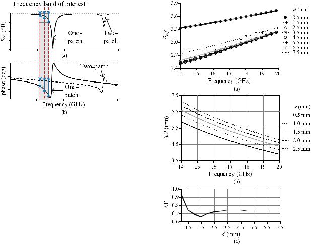
The operational model of the patch in the rectangular waveguide using the existing planar technologies was adopted. During the analysis, it is noticed that depending on the location d, the patch either operates as a microstrip or in a suspended stripline mode. Therefore, the length R could be estimated using either technology depending on d. Fig. 5(a) and (b) shows the simulated effective dielectric constant εeff and the half wavelength λ/2 for different values of d and widths w, illustrating that the patch operates either
as |
a microstrip or a suspended stripline. As can be seen |
in |
Fig. 5(a), when d is less than 2.5 mm, distinct εeff |
for |
different values of d are obtained, and therefore is a |
Fig. 5. Simulated (a) effective dielectric constant (εeff ) with different d,
(b) half wavelength (λ/2) with different patch width w in mm versus frequency, and (c) AF when w = 0.5 mm.
microstrip operation. However, when d is greater than 2.5 mm, εeff remains similar for different d values, demonstrating evidence for a suspended stripline behaviour. As the patch is half-wavelength long with two open-circuit ends, fringing capacitance loading must be taken into consideration when calculating the physical length R. Therefore, R needs to be adjusted to account for these fringing capacitances. For example, for width w = 0.5 mm, the corresponding adjustment factor (AF) is calculated and shown in Fig. 5(c). This factor is inversely proportional to the patch width. In general, a wider patch results in a smaller adjustment, and vice versa. With the understanding of the general design principle and the method for calculating the patch dimensions for different frequencies of operation, it is then possible to consider the optimal conditions for the oneand two-patch cases. These conditions should allow the equivalent detuning element to provide the necessary effective phase shift (or change in resonant frequency) for the one-patch case while introducing minimum loss for the twopatch case in a resonator. A bandstop filter design modeling method is implemented here even though the detuning element is operating at off-resonance. As shown in Fig. 3(b), such a model uses a shunt impedance Zr due to the patch and line impedance Z L to incorporate the length of the waveguide. The inductance Lr , hence the reactance xr , could then be related to

This article has been accepted for inclusion in a future issue of this journal. Content is final as presented, with the exception of pagination.
4 |
|
|
|
|
|
|
IEEE TRANSACTIONS ON MICROWAVE THEORY AND TECHNIQUES |
||||||||
|
|
|
|
|
|
|
|
|
|
|
|
|
|
|
|
|
|
|
|
|
|
|
|
|
|
|
|
|
|
|
|
|
|
|
|
|
|
|
|
|
|
|
|
|
|
|
|
|
|
|
|
|
|
|
|
|
|
|
|
|
|
|
|
|
|
|
|
|
|
|
|
|
|
|
|
|
|
|
|
|
|
|
|
|
|
|
|
|
|
|
|
|
|
|
|
|
|
|
|
|
|
|
|
|
|
|
|
|
|
|
|
|
|
|
|
|
|
|
|
|
|
|
|
|
|
|
|
|
|
|
|
|
|
|
|
|
|
|
|
|
|
|
|
|
|
|
|
|
|
|
|
|
|
|
|
|
|
|
|
|
|
|
|
|
|
|
|
|
|
|
|
|
|
|
|
Fig. 6. Normalized reactance xr /Z0 and 3-dB bandwidth versus d.
Fig. 7. Normalized loss induced to the desired frequency versus the normalized reactance xr /Z0 with different Rr .
the prototype filter g-values and the 3-dB bandwidth, as shown in (1) [65]. Again, with w set to 0.5 mm, a normalized reactance xr /Z0 is calculated by simulating the patch for different d locations, and is plotted in Fig. 6. As can be noticed, xr /Z0 reduces significantly once d increases beyond 0.5 mm. From Fig. 6, it can be noticed that the bandwidth of the bandstop notch becomes very large as xr /Z0 decreases
|
Zr (ω) = Rr |
+ j ω Lr + 1/ j ωCr |
|
|||||||||
|
|
xr |
= |
ωr |
|
d Zr (ω) |
|ωr |
|
||||
|
|
2 |
|
dω |
|
|||||||
|
|
|
|
= ωr Lr |
|
|
|
|||||
|
|
|
|
= |
Z0 |
|
fr |
|
|
|
||
|
|
|
|
2 f3 dB |
|
|
|
|
||||
|
|
|
|
|
Z0 |
1 |
|
|
|
|
(1) |
|
|
|
|
|
|
|
|
|
|
|
|||
|
|
|
|
gn+1g f |
|
|
||||||
|
|
|
|
= |
|
|
|
|
||||
S21( fBPF) = |
|
2Zr ( fBPF) |
|
(2) |
||||||||
2Zr ( fBPF) + Z0 |
||||||||||||
S |
( f |
|
) |
= |
|
|
−Z0 |
|
|
(3) |
||
|
2Zr ( fBPF) + Z0 |
|||||||||||
11 |
|
BPF |
|
|
||||||||
Loss( fBPF) |
= 1 − |S11( fBPF)|2 − |S21( fBPF)|2. |
(4) |
||||||||||
1) Two-Patch OFF-State Considerations: The primary purpose of the detuning element is to achieve an effective phase detuning at the ON-state (one-patch), while introducing minimal loss to the bandpass filter at the OFF-state (twopatch). As discussed in the Introduction, although many devices reported in the literature are capable of achieving the necessary detuning, they introduce relatively high loss. Therefore, the critical challenge is to achieve minimal loss for a waveguide or a waveguide bandpass filter during the OFF-state of the detuning element. By using (1)–(4), this loss at different frequencies ( fBPF) can be calculated. Fig. 7 shows the loss
Fig. 8. Plot of S21 in dB versus the change in phase S21 for different Rr .
with different normalized reactances xr /Z0 and resistances Rr . Here, this fBPF is assumed to be 15% away from the bandstop notch frequency fr , where the offset percentage is calculated as ( fr − fBPF)/ fBPF. From Fig. 7, it is evidenced that as long as xr /Z0 is kept large, the loss due to the bandstop notch is minimized even when the bandstop notch is inherently lossy. For example, from the simulations, even when the resistance Rr is as large as 20 , the loss due to the bandstop notch is only less than 1%, whereas xr /Z0 is higher than 20. In general, it is correct to assume that if the offset frequency is larger than 15%, the loss contribution from the bandstop notch reduces and vice versa.
2) One-Patch ON-State Considerations: Although the
ON-state (one-patch) and OFF-state (two-patch) are assumed to have different bandstop notch frequencies, their xr /Z0 values are similar as their patch widths w are the same. With the optimal range of xr /Z0 decided using the OFF-state, it is possible to determine the ON-state (one-patch) length R to achieve different effective detuning phases in a resonator. To quantify the amount of effective detuning, the S-parameter changes induced by the patch in a waveguide using (2) are evaluated with xr /Z0 set to 20; in particular, the phase shift is recorded as a reference. The amount of phase shift versus waveguide S21, in dB, is illustrated in Fig. 8. As can be noticed, a larger phase shift could be achieved with smaller S21 values (closer to the notch frequency) indicating a larger effective detuning when incorporating this patch into the resonant cavity (RC). Similarly, further away from the notch results in a smaller effective detuning. It can also be noticed that the loss in the notch also affects the amount of achievable phase shift, as suggested by Fig. 8. When the resistance Rr in the patch increases, the amount of achievable phase shift reduces proportionally. Therefore, the Q-factor of the patch also influences the possible phase shift, hence indicating an impact on effective detuning.
B. MEMS Implementation
Fig. 9 illustrates the design of the MEMS-based waveguide detuning. The switchable MEMS detuning elements are designed on an alumina wafer with εr = 9.9 and 635-μm thickness. The elements are attached at d = 0.5 mm distance from one of the narrow sidewalls and have a height H + 2Hadd, in which Hadd adds a slightly longer length than the narrow waveguide edge to assist affixing them to the

This article has been accepted for inclusion in a future issue of this journal. Content is final as presented, with the exception of pagination.
CHAN et al.: Ku-BAND CHANNEL AGGREGATION WAVEGUIDE FILTERS |
5 |
Fig. 9. MEMS tuning elements inserted in a rectangular waveguide. (a) Layout on the wafer for the two designs for two channels, CH1 (14.25 GHz) and CH2 (16.25 GHz). (b) Zoomed-in view of the MEMS switches showing all the dimensions.
TABLE I
LIST OF DIMENSIONS IN FIG. 9
Fig. 10. Current distribution of a stripline housed in a WR62 rectangular waveguide with d = 0.5 mm.
waveguide cavities as shown in Fig. 9(a). Two separate circuits are designed to detune the filters at two different channels on individual demand. The CH1 circuit aims to detune the 14.25-GHz bandpass filter, while the CH2 circuit has the role of detuning the 16.25-GHz bandpass filter. The dimensions of these devices are listed in Table I. The design of the switchable detuning elements consists of three main parts: the patch, biasing pad, and MEMS switches located in the middle of the patch. The elements, with lengths RH and RL in Fig. 9(a), are the patches. From the analysis in the previous section, it is concluded that they operate as microstrip lines, as d is 2.5 mm. The MEMS switches are of cantilever type, and they have anchors at the bottom patches and contact points to the top patches, as shown in Fig. 9(b). Fig. 10 illustrates the simulated patch current distribution with w = 0.5 mm. As can be seen, the majority of the current is concentrated along the two edges. Therefore, in order to maintain a similar current distribution as with the addition of MEMS switches, the switches are placed on the two edges. More switches or broader switches could have been utilized. However, the increase in the switch number also reduces the isolation of the two-patch case. Also, in order to keep the two-patch bandstop notch to be at least 15%
normalized frequency away from the desired bandpass filter center frequency, only two switches are employed.
The biasing pads, with dimensions BH and BL , have to be designed with consideration as they exhibit bandstop notches themselves, just like the detuning patches. Therefore, when putting together the biasing pad with the patch, two bandstop notches located at different frequencies are expected typically. Hence, BH and BL have to be selected to produce notches further away from the waveguide channel frequency compared to the OFF-state patches. In addition, when the MEMS switches are actuated, due to the proximity of the cantilever beams with the biasing line and pad, strong coupling occurs, resulting in a single bandstop notch instead of two. Therefore, the ON-state bandstop notch is slightly modified. To accommodate these, BH and BL are designed to have different dimensions in the upper and lower channels. Fig. 11 shows the simulations of MEMS detuning elements for the two channels where the highlighted (in grey) frequency ranges are the corresponding passbands of waveguide bandpass filters. In Fig. 11(a) and (c), the magnitude of the S-parameters of the detuning elements are shown for both ON- and OFF-states. As it can be noticed, the ON-state of the two designs each has a single bandstop notch adjacent to the upper side of their passbands. Fig. 11(b) and (d) shows that due to the notches, the phase changes between the ON- and OFF-states are more than 10◦ for both designs at the center frequency of the passbands. These ON- and OFF-state S-parameter differences guarantee an effective phase shift (or change in resonant frequency) between the states when using them within waveguide resonators. When examining the OFF-states, two bandstop notches from each design are observed, where the lower frequency notch is generated from the patch and the higher frequency one is from the biasing pad. Nevertheless, these notches are at least 15% away from the center frequency of the passbands. Besides, when calculating their normalized reactance using their 3-dB bandwidths, values much larger than 20 in the range of 100 is obtained, resulting in loss contributions of <0.05% to the passbands of the bandpass filters.
It should be noted that it is also possible to place the ON-state bandstop notch at the lower side of the passbands instead of the upper side while achieving a similar amount of phase shift. However, when placing the ON-state bandstop notch at a lower frequency, the corresponding OFF-state bandstop notch also moves to a lower frequency resulting in a reduction of the offset frequency away from the waveguide passband. This introduces higher loss to the waveguide bandpass filter according to our analysis, and hence this option is undesirable.
C. Design of Reconfigurable Two-Channel Filter
The reconfigurable switchable filter, enabling channel aggregation, in rectangular waveguide technology, is designed and optimized using Mician μWave Wizard and ANSYS HFSS. Fig. 12(a) shows the schematic of the system. It consists of two identical waveguide manifolds at the input and output ports and two eight-pole E-plane iris waveguide bandpass filters. Fig. 12(a) illustrates the side view of the manifolds from the

This article has been accepted for inclusion in a future issue of this journal. Content is final as presented, with the exception of pagination.
6 |
|
|
|
|
|
|
|
|
|
|
|
|
|
|
|
|
IEEE TRANSACTIONS ON MICROWAVE THEORY AND TECHNIQUES |
||||||||||||||||||||
|
|
|
|
|
|
|
|
|
|
|
|
|
|
|
|
|
|
|
|
|
|
|
|
|
|
|
|
|
|
|
|
|
|
|
|
|
|
|
|
|
|
|
|
|
|
|
|
|
|
|
|
|
|
|
|
|
|
|
|
|
|
|
|
|
|
|
|
|
|
|
|
|
|
|
|
|
|
|
|
|
|
|
|
|
|
|
|
|
|
|
|
|
|
|
|
|
|
|
|
|
|
|
|
|
|
|
|
|
|
|
|
|
|
|
|
|
|
|
|
|
|
|
|
|
|
|
|
|
|
|
|
|
|
|
|
|
|
|
|
|
|
|
|
|
|
|
|
|
|
|
|
|
|
|
|
|
|
|
|
|
|
|
|
|
|
|
|
|
|
|
|
|
|
|
|
|
|
|
|
|
|
|
|
|
|
|
|
|
|
|
|
|
|
|
|
|
|
|
|
|
|
|
|
|
|
|
|
|
|
|
|
|
|
|
|
|
|
|
|
|
|
|
|
|
|
|
|
|
|
|
|
|
|
|
|
|
|
|
|
|
|
|
|
|
|
|
|
|
|
|
|
|
|
|
|
|
|
|
|
|
|
|
|
|
|
|
|
|
|
|
|
|
|
|
|
|
|
|
|
|
|
|
|
|
|
|
|
|
|
|
|
|
|
|
|
|
|
|
|
|
|
|
|
|
|
|
|
|
|
|
|
|
|
|
|
|
|
|
|
|
|
|
|
|
|
|
|
|
|
|
|
|
|
|
|
|
|
|
|
|
|
|
|
|
|
|
|
|
|
|
|
|
|
|
|
|
|
|
|
|
|
|
|
|
|
|
|
|
|
|
|
|
|
|
|
|
|
|
|
|
|
|
|
|
|
|
|
|
|
|
|
|
|
|
|
|
|
|
|
|
|
|
|
|
|
|
|
|
|
|
|
|
|
|
|
|
|
|
|
|
|
|
|
|
|
|
|
|
|
|
|
|
|
|
|
|
|
|
|
|
|
|
|
|
|
|
|
|
|
|
|
|
|
|
|
|
|
|
|
|
|
|
|
|
|
|
|
|
|
|
|
|
|
|
|
|
|
|
|
|
|
|
|
|
|
|
|
|
|
|
|
|
|
|
|
|
|
|
|
|
|
|
|
|
|
|
|
|
|
|
|
|
|
|
|
|
|
|
|
|
|
|
|
|
|
|
|
|
|
|
|
|
|
|
|
|
|
|
|
|
|
|
|
|
|
|
|
|
|
|
|
|
|
|
|
|
|
|
|
|
|
|
|
|
|
|
|
|
|
|
|
|
|
|
|
|
|
|
|
|
|
|
|
|
|
|
|
|
|
|
|
|
|
|
|
|
|
|
|
|
|
|
|
|
|
|
|
|
|
|
|
|
|
|
|
|
|
|
|
|
|
|
|
|
|
|
|
|
|
|
|
|
|
|
|
|
|
|
|
|
|
|
|
|
|
|
|
|
|
|
|
|
|
|
|
|
|
|
|
|
|
|
|
|
|
|
|
|
|
|
|
|
|
|
|
|
|
|
|
|
|
|
|
|
|
|
|
|
|
|
|
|
|
|
|
|
|
|
|
|
|
|
|
|
|
|
|
|
|
|
|
|
|
|
|
|
|
|
|
|
|
|
|
|
|
|
|
|
|
|
|
|
|
|
|
|
|
|
|
|
|
|
|
|
|
|
|
|
|
|
|
|
|
|
|
|
|
|
|
|
|
|
|
|
|
|
|
|
|
|
|
|
|
|
|
|
|
|
|
|
|
|
|
|
|
|
|
|
|
|
|
|
|
|
|
|
|
|
|
|
|
|
|
|
|
|
|
|
|
|
|
|
|
|
|
|
|
|
|
|
|
|
|
|
|
|
|
|
|
|
|
|
|
|
|
|
|
|
|
|
|
|
|
|
|
|
|
|
|
|
|
|
|
|
|
|
|
|
|
|
|
|
|
|
|
|
|
|
|
|
|
|
|
Fig. 11. Responses of the MEMS switchable planar resonators introduced in the rectangular waveguide. CH1 design. (a) S-parameters and (b) transmission phase angles in ON- and OFF-states. CH2 design (c) S-parameters and
(d) transmission phase angles, in ON- and OFF-states.
narrow edge of the rectangular waveguide with the dimension labels shown. The manifold consists of an H-plane iris near the input/output port, an E-type T junction, and two waveguide connections with lengths L f 1 and L f 2 corresponding to
Fig. 12. Design of the two-channel reconfigurable filter. (a) System view showing the channel filters and the manifolds with dimension labels.
(b)Bandpass filter coupling model showing the resonant cavity number.
(c)Top view of an eight-pole E-plane iris waveguide bandpass, with dimension labels.
TABLE II
LIST OF DIMENSIONS IN FIG. 12
the lowand high-band channel filter connections. As the reflection of each channel filter also affects the other channel connected to the manifold, the manifold can be designed using [66]. The two channel filters are designed based on typical E-plane iris waveguide band-pass filter architecture with the top view shown in Fig. 12(c) and all dimensions listed in Table II.
In our design, the only modification to the traditional iris waveguide filter is the introduction of the proposed switchable detuning elements in some of the resonant cavities with the cavity named according to Fig. 12(b).
The waveguide resonant cavities with the embedded detuning elements can be considered as step-impedance resonators as represented in Fig. 13, where the transmission line in the

This article has been accepted for inclusion in a future issue of this journal. Content is final as presented, with the exception of pagination.
CHAN et al.: Ku-BAND CHANNEL AGGREGATION WAVEGUIDE FILTERS |
7 |
|||||||||||||||||||||||||||||||||||||||||||||||||||||||||||||||||||||||
|
|
|
|
|
|
|
|
|
|
|
|
|
|
|
|
|
|
|
|
|
|
|
|
|
|
|
|
|
|
|
|
|
|
|
|
|
|
|
|
|
|
|
|
|
|
|
|
|
|
|
|
|
|
|
|
|
|
|
|
|
|
|
|
|
|
|
|
|
|
|
|
|
|
|
|
|
|
|
|
|
|
|
|
|
|
|
|
|
|
|
|
|
|
|
|
|
|
|
|
|
|
|
|
|
|
|
|
|
|
|
|
|
|
|
|
|
|
|
|
|
|
|
|
|
|
|
|
|
|
|
|
|
|
|
|
|
|
|
|
|
|
|
|
|
|
|
|
|
|
|
|
|
|
|
|
|
|
|
|
|
|
|
|
|
|
|
|
|
|
|
|
|
|
|
|
|
|
|
|
|
|
|
|
|
|
|
|
|
|
|
|
|
|
|
|
|
|
|
|
|
|
|
|
|
|
|
|
|
|
|
|
|
|
|
|
|
|
|
|
|
|
|
|
|
|
|
|
|
|
|
|
|
|
|
|
|
|
|
|
|
|
|
|
|
|
|
|
|
|
|
|
|
|
|
|
|
|
|
|
|
|
|
|
|
|
|
|
|
|
|
|
|
|
|
|
|
|
|
|
|
|
|
|
|
|
|
|
|
|
|
|
|
|
|
|
|
|
|
|
|
|
|
|
|
|
|
|
|
|
|
|
|
|
|
|
|
|
|
|
|
|
|
|
|
|
|
|
|
|
|
|
|
|
|
|
|
|
|
|
|
|
|
|
|
|
|
|
|
|
|
|
|
|
|
|
|
|
|
|
|
|
|
|
|
|
|
|
|
|
|
|
|
|
|
|
|
|
|
|
|
|
|
|
|
|
|
|
|
|
|
|
|
|
|
|
|
|
|
|
|
|
|
|
|
|
|
|
|
|
|
|
|
|
|
|
|
|
|
|
|
|
|
|
|
|
|
|
|
|
|
|
|
|
|
|
|
|
|
|
|
|
|
|
|
|
|
|
|
|
|
|
|
|
|
|
|
|
|
|
|
|
|
|
|
|
|
|
|
|
|
|
|
|
|
|
|
|
|
|
|
|
|
|
|
|
|
|
|
|
|
|
|
|
|
|
|
|
|
|
|
|
|
|
|
|
|
|
|
|
|
|
|
|
|
|
|
|
|
|
|
|
|
|
|
|
|
|
|
|
|
|
|
|
|
|
|
|
|
|
|
|
|
|
|
|
|
|
|
|
|
|
|
|
|
|
|
|
|
|
|
|
|
|
|
|
|
|
|
|
|
|
|
|
|
|
|
|
|
|
|
|
|
|
Fig. 13. Series resonator circuit model for resonator cavities consisting of the detuning element at OFF-state.
center is contributed by the OFF-state of the MEMS detuning element as in Fig. 3(d). The characteristic impedance Z L includes the circuit parameters from the metal patches on the substrate as well as the parasitic of the transitions from all the air-filled waveguide to the partially dielectric-filled waveguide. However, as the carrier substrate is located very close to the narrow sidewall and is relatively thin, contributing only 4% of the total waveguide volume, together with the minimal impact from the planar circuit, Z L and βL are only slightly different from Z0 and β0, resulting in the step impedance ratio Z0/Z L being close to 1. Hence, for determining the resonant condition that requires Zin = 0 for a series resonance [67], the total phase length 2β0l0 + βLlL only differs a little from 180◦. Eigenvalue simulations have been performed with these resonators and are compared with typical waveguide resonators. From the simulations, when the switches are not actuated, the theoretical Q-factors are 3300 and 3430 at 14.25 and 16.25 GHz, respectively, whereas typical waveguide resonators have Q-factors of 5580 and 5430 at these frequencies. When the switches are actuated, the resonant frequencies become 13.46 and 15.49 GHz. These detuned resonant frequencies could also be considered as having detuned phases of 20.39◦ and 13.91◦ from 180◦ at their original resonant frequencies.
To determine how many and in which resonant cavities the detuning elements should be placed, two questions must be addressed. First is the desired isolation necessary after detuning the corresponding filter. The second is the out-of- band impact of the one channel to the adjacent channel and the proximity of the channels.
Regarding the isolation, it has been found that the amount of achievable isolation depends on two factors: 1) the number of detuned cavities and their location within the filter and 2) the detuned phase (or the detuned frequency). For example, for an eight-pole iris waveguide filter, the ideal RC length is nλ/2, where n is an integer. Therefore, the multiples of 180◦ are valid phase lengths for the RC resulting in the maximum possible detuned phase of ±90◦. Fig. 14 demonstrates the achievable isolation versus detuning phase in the eight-pole bandpass filter with a different combination of detuned cavities with different detuning phases. It should be noted that the OFF-state suppression presented in Fig. 14 is only valid for an eight-pole filter with a bandwidth of 3%–3.5% and with the assumption that its resonators are lossless with an infinite Q-factor. As could be noticed, the more the detuned cavities are, the higher the isolation. In Fig. 14, RC 1 indicates the first filter RC is detuned; RC 4, 5 signify detuning resonant cavities four and five, respectively, and RC 1–8 indicates detuning all eight resonant cavities of the eight-pole filter. In addition, the
Fig. 14. Achievable isolation in an eight-pole filter with different combinations of detuned resonators versus detuning phase.
Fig. 15. Change of reflection phase versus out-of-band isolation of an eight-pole filter with different combinations of detuned resonant cavities.
more inward (away from the I/O ports) the detuned cavities in the filter are, the higher the achievable isolation. In general, these rules apply to all bandpass filter with different orders. To address the first question, 40-dB isolation is targeted in this article. According to Fig. 14 and the achievable effective detuning phase from the MEMS-based detuning elements, at least two resonant cavities have to be detuned. To address the second question, the out-of-band impact from a detuned filter to other filters connected to the manifolds, the reflected phases of the eight-pole filter with different detuned resonant cavities were simulated. Fig. 15 illustrates the reflected phase change of different combinations of detuned resonant cavities observed at different out-of-band isolation points.
From Fig. 15, it is evident that detuning RC 1 is not ideal, as any detuning combination involving RC 1 induces a significant change in the reflected phase. Similar to Fig. 14, the more inward the detuned resonant cavities are, the smaller is the change in the reflected phase.
The effect of different detuning combinations in one filter to the other is also observed in S-parameters. In particular, the effect on the S-parameters of the upper band is illustrated in Fig. 16, as the lower band filter is detuned. From Fig. 16, it can be noticed that when all the resonant cavities (RC 1–RC 8) are detuned, the upper band return loss degrades the most (the finest dotted line). Whereas detuning RC 1 only or detuning from RC 1 to RC 7 showed no significant differences to the upper band return loss. Moreover, detuning

This article has been accepted for inclusion in a future issue of this journal. Content is final as presented, with the exception of pagination.
8 |
|
|
|
|
|
|
|
|
|
|
|
|
|
|
|
|
IEEE TRANSACTIONS ON MICROWAVE THEORY AND TECHNIQUES |
|
|
|
|
|
|
|
|
|
|
|
|
|
|
|
|
|
|
|
|
|
|
|
|
|
|
|
|
|
|
|
|
|
|
|
|
|
|
|
|
|
|
|
|
|
|
|
|
|
|
|
|
|
|
|
|
|
|
|
|
|
|
|
|
|
|
|
|
|
|
|
|
|
|
|
|
|
|
|
|
|
|
|
|
|
|
|
|
|
|
|
|
|
|
|
|
|
|
|
|
|
|
|
|
|
|
|
|
|
|
|
|
|
|
|
|
|
|
|
|
|
|
|
|
|
|
|
|
|
|
|
|
|
|
|
|
|
|
|
|
|
|
|
|
|
|
|
|
|
|
|
|
|
|
|
|
|
|
|
|
|
|
|
|
|
|
|
|
|
|
|
|
|
|
|
|
|
|
|
|
|
|
|
|
|
|
|
|
|
|
|
|
|
|
|
|
|
|
|
|
|
|
|
|
|
|
|
|
|
|
|
|
|
|
|
|
|
|
|
|
|
|
|
|
|
|
|
|
|
|
|
|
|
|
|
|
|
|
|
|
|
|
|
|
|
|
|
|
|
|
|
|
|
|
|
|
|
|
|
|
|
|
|
|
|
|
|
|
|
|
|
|
|
|
|
|
|
|
|
|
|
|
|
|
|
|
|
|
|
|
|
|
|
|
|
|
|
|
|
|
|
|
|
|
|
|
Fig. 16. Simulated S-parameters of different combinations for observing the relationship between detuned cavities and the out-of-band isolation.
Fig. 17. Complex E-field distribution of (a) filter with MEMS detuning elements at OFF-state in RC 4 and 5, (b) typical filter without any detuning elements, (c) filter with MEMS-detuning elements at ON-state in RC 4 and 5, and (d) typical filter with RC 4 and 5 detuning by reducing the phase lengths.
any cavities from RC 2 onward shows minimum changes to the return loss of the upper band.
Therefore, as a conclusion, two switchable detuning elements are designed to locate in the innermost RC 4 and RC 5.
To further validate the detuning technique, simulations of the electromagnetic field distributions of an eight-pole filter with detuning elements incorporated in RC 4 and 5 at both states are compared to the typical waveguide filters.
Fig. 17(a) shows the magnitude of the complex E-field distribution of the filter when the MEMS switches are set to the OFF-state. It could be noticed that no significant difference between the E-field distribution could be observed in RC 4 and 5 of Fig. 17(a) and (b). With the switches set to the ON-state, the electrical properties of RC 4 and 5 are changed. These changes show similar behavior, Fig. 17(c) and (d), to a typical filter with significant phase length detuning in RC 4 and 5. Although the complex E-field in Fig. 17(c) swings toward the MEMS detuning element in RC 4, no strong E-field is observed to indicate the in-band bandstop notch.
Fig. 18. (a) Fabricated aluminium housing in two halves. (b) RC4 and 5 with the MEMS detuning elements and extra openings for insertion. (c) MEMS detuning elements only. (d) Zoomed-in view showing the MEMS switches.
III. FABRICATION AND MEASUREMENTS
The two-channel aggregation waveguide filter fabricated using aluminum and in-house CNC machining are shown in Fig. 18. The housing is designed as two separate pieces; the bottom piece has additional openings in the fourth (RC 4) and fifth cavities (RC 5) for both the low-frequency 14.25 GHz (CH1) and high-frequency 16.25 GHz (CH2) channel filters as in Fig. 16(a). These extra openings in the resonant cavities accommodate the MEMS-based-detuning elements as shown in Fig. 18(b). Also, within these modified cavities, small through holes on one of the narrow sidewalls are drilled to pass the dc biasing wires for controlling the MEMS switches. These holes only have diameters of 1 mm to avoid the leakage of electromagnetic fields. The MEMS-based detuning elements shown in Fig. 18(c) and shown as a zoomed-in view in Fig. 18(d) are fabricated with a simplified all-gold surface microfabrication process similar to [68]. In this fabrication process, all lossy metal layers such as Cr were avoided as the lossy materials can introduce additional conduction loss and significantly degrade the Q-factor of the waveguide resonant cavities. To avoid parasitics, very small biasing wires, AWG30, with a diameter of 254 μm were selected and were adhered to the biasing pads with wire glue.

This article has been accepted for inclusion in a future issue of this journal. Content is final as presented, with the exception of pagination.
CHAN et al.: Ku-BAND CHANNEL AGGREGATION WAVEGUIDE FILTERS |
9 |
|||||||||||||||||||||||||||||
|
|
|
|
|
|
|
|
|
|
|
|
|
|
|
|
|
|
|
|
|
|
|
|
|
|
|
|
|
|
|
|
|
|
|
|
|
|
|
|
|
|
|
|
|
|
|
|
|
|
|
|
|
|
|
|
|
|
|
|
|
|
|
|
|
|
|
|
|
|
|
|
|
|
|
|
|
|
|
|
|
|
|
|
|
|
|
|
|
|
|
|
|
|
|
|
|
|
|
|
|
|
|
|
|
|
|
|
|
|
|
|
|
|
|
|
|
|
|
|
|
|
|
|
|
|
|
|
|
|
|
|
|
|
|
|
|
|
|
|
|
|
|
|
|
|
|
|
|
|
|
|
|
|
|
|
|
|
|
|
|
|
|
|
|
|
|
|
|
|
|
|
|
|
|
|
|
|
|
|
|
|
|
|
|
|
|
|
|
|
|
|
|
|
|
|
|
|
|
|
|
|
|
|
|
|
|
|
|
|
|
|
|
|
|
|
|
|
|
|
|
|
|
|
|
|
|
|
|
|
|
|
|
|
|
|
|
|
|
|
|
|
|
|
|
|
|
|
|
|
|
|
|
|
|
|
|
|
|
|
|
|
|
|
|
|
|
|
|
|
|
|
|
|
|
|
|
|
|
|
|
|
|
|
|
|
|
|
|
|
|
|
|
|
|
|
|
|
|
|
|
|
|
|
|
|
|
|
|
|
|
|
|
|
|
|
|
|
|
|
|
|
|
|
|
|
|
|
|
|
|
|
|
|
|
|
|
|
|
|
|
|
|
|
|
|
|
|
|
|
|
|
|
|
|
|
|
|
|
|
|
|
|
|
|
|
|
|
|
|
|
|
|
|
|
|
|
|
|
|
|
|
|
|
|
|
|
|
|
|
|
|
|
|
|
|
|
|
|
|
|
|
|
|
|
|
|
|
|
|
|
|
|
|
|
|
|
|
|
|
|
|
|
|
|
|
|
|
|
|
|
|
|
|
|
|
|
|
|
|
|
|
|
|
|
|
|
|
|
|
|
|
|
|
|
|
|
|
|
|
|
|
|
|
|
|
|
|
|
|
|
|
|
|
|
|
|
|
|
|
|
|
|
|
|
|
|
|
|
|
|
|
|
|
|
|
|
|
|
|
|
|
|
|
|
|
|
|
|
|
|
|
|
|
|
|
|
|
|
|
|
|
|
|
|
|
|
|
|
|
|
|
|
|
|
|
|
|
|
|
|
|
|
|
|
|
|
|
|
|
|
|
|
|
|
|
|
|
|
|
|
|
|
|
|
|
|
|
|
|
|
|
|
|
|
|
|
|
|
|
|
|
|
|
|
|
|
|
|
|
|
|
|
|
|
|
|
|
|
|
|
|
|
|
|
|
|
|
|
|
|
|
|
|
|
|
|
|
|
|
|
|
|
|
|
|
|
|
|
|
|
|
|
|
|
|
|
|
|
|
|
|
|
|
|
|
|
|
|
|
|
|
|
|
|
|
|
|
|
|
|
|
|
|
|
|
|
|
|
|
|
|
|
|
|
|
|
|
|
|
|
|
Fig. 19. Measured and simulated response of the reconfigurable switchable filter in four states. (a) (00) state when both channels are switched OFF.
(b) (01) state when only the low band is turned off. (c) (10) state when the high band is switched OFF. (d) (11) state when both channels are ON.
The fabricated filter was measured using Agilent E8346C with coaxial to waveguide adapters. The desired four states were achieved with an actuation voltage of 20 V to enable
Fig. 20. Zoomed-in view of measured and simulated S21(dB) of the reconfigurable switchable filter in three states. (a) (01) state when only the CH2 is enabled. (b) (10) state when CH1 is enabled. (c) (11) state when both channels are enabled.
different channel filters, e.g., (00), (01), (10), and (11). This actuation voltage can support up to 15-W input power to the waveguide filter before self-actuation. It should be noted that much higher power handling capability can be achieved with these MEMS detuning elements. It is a tradeoff between actuation voltage of the MEMS switch and the power handling of the system. In theory, by increasing the thickness of the cantilever beam of the MEMS switches, the actuation voltage can be increased to 200 V and beyond. As a guideline, from HFSS simulations, with an input power of the filter set to 100 and 300 W, the maximum induced voltage across the cantilever beam and the actuation pad is only 75 and 175 V, respectively.
Fig. 19(a) shows the measured S-parameters of state (00) in agreement with the simulations, where better than 35-dB isolation was achieved over the two channels. Fig. 19(b) and (c) show the measured S-parameters of the two states (01) and (10). In Fig. 19(b), with CH1 disabled and CH2 enabled, i.e., state (01), the CH1 isolation response is better than 38 dB, in agreement with the simulations. The enabled CH2 has a bandpass filter response with insertion loss better than 2 dB, which corresponds to around 800 Q-factor. The return loss is also better than 15 dB in the passband. Fig. 19(c) shows the S-parameters of state (10) with CH1 enabled and CH2 disabled. The measured passband insertion loss for CH1 is again better than 2 dB while maintaining better than 15-dB return loss. CH2 isolation is better than 35 dB, similar to the simulation. Fig. 19(d) showed the measured S-parameters when both channels CH1, CH2, are enabled, i.e., state (11). When comparing the in-band bandpass filter responses of all the states given in Fig. 20, it could be noticed that the S21 responses are very similar regardless of the states and therefore further validating the design equations and simulations.

This article has been accepted for inclusion in a future issue of this journal. Content is final as presented, with the exception of pagination.
10 |
IEEE TRANSACTIONS ON MICROWAVE THEORY AND TECHNIQUES |
TABLE III
COMPARISON OF THE PROPOSED FILTER TO THE LITERATURE
In all states, the isolation discrepancies between simulations and measurements are due to the differences in the metal loss of the MEMS-based-detuning elements and the associated contact losses of MEMS switches. All these losses degraded the isolations and hence the disagreement. The return loss disagreements in all the states are primarily due to fabrication tolerance. The Q-factor degradation between simulations and measurements are primarily due to the in-house manufacturing and assembly issues.
Table III provides a comparison of the proposed filter with other existing reconfigurable filters highlighting the significance of this article. It illustrates that although a significant research effort has been invested into reconfigurable filters achieving excellent tuning range and Q-factor, minimal effort has been put into designing channel aggregation filters. To the authors’ knowledge, no 3-D type channel aggregation filter has ever been reported with only very few planar designs reported [61], [62].
IV. CONCLUSION
In this article, we offer, for the first time, a channel aggregation waveguide switchable bandpass filter using MEMSbased detuning elements. The novelty consists of loading the resonant cavities of the channel filters with MEMS-based detuning elements that operate at off-resonance. The channel aggregation capability of a two-channel filter system was demonstrated. By turning the MEMS switches ON- and OFF-, the system can offer a combination of four different states, (00), (01), (10), and (11), i.e., all-rejects, upper band only, lower band only, and dual band. The four states were measured, and the isolation response for any disabled channels was found to be better than 35 dB in both CH1 and CH2. The measured passband insertion loss in states (01), (10), and (11) was better than 2 dB, equivalent to over 800 Q-factor, while maintaining better than 15-dB return loss.
ACKNOWLEDGMENT
This work was carried out at the UNSW ANFF in the NSW Node and at the Melbourne Centre for Nanofabrication (MCN)
in the Victorian Node of the Australian National Fabrication Facility (ANFF).
REFERENCES
[1]A. C. Guyette, “Theory and design of intrinsically switched multiplexers with optimum phase linearity,” IEEE Trans. Microw. Theory Techn., vol. 61, no. 9, pp. 3254–3264, Sep. 2013.
[2]C. I. Mobbs, “The use of matched four-port filters to realize switched multiplexer having low amplitude and group delay ripple,” IEEE Trans. Microw. Theory Techn., vol. MTT-35, no. 12, pp. 1183–1191, Dec. 1987.
[3]L. Gao, X. Y. Zhang, B.-J. Hu, and Q. Xue, “Novel multi-stub loaded resonators and their applications to various bandpass filters,” IEEE Trans. Microw. Theory Techn., vol. 62, no. 5, pp. 1162–1172, May 2014.
[4]E. J. Naglich, J. Lee, D. Peroulis, and W. J. Chappell, “A tunable bandpass-to-bandstop reconfigurable filter with independent bandwidths and tunable response shape,” IEEE Trans. Microw. Theory Techn., vol. 58, no. 12, pp. 3770–3779, Dec. 2010.
[5]R. Gómez-García and A. C. Guyette, “Reconfigurable multi-band microwave filters,” IEEE Trans. Microw. Theory Techn., vol. 63, no. 4,
pp.1294–1307, Apr. 2015.
[6]Y.-H. Cho and G. M. Rebeiz, “0.73–1.03-GHz tunable bandpass filter with a reconfigurable 2/3/4-pole response,” IEEE Trans. Microw. Theory Techn., vol. 62, no. 2, pp. 290–296, Feb. 2014.
[7]X. Y. Zhang, C. H. Chan, Q. Xue, and B. J. Hu, “RF tunable bandstop filters with constant bandwidth based on a doublet configuration,” IEEE Trans. Ind. Electron., vol. 59, no. 2, pp. 1257–1265, Feb. 2012.
[8]N. Zahirovic, S. Fouladi, R. R. Mansour, and M. Yu, “Tunable suspended substrate stripline filters with constant bandwidth,” in IEEE MTT-S Int. Microw. Symp. Dig., Baltimore, MD, USA, Aug. 2011, pp. 1–4.
[9]X. Y. Zhang, Q. Xue, C. H. Chan, and B. J. Hu, “Low-loss frequencyagile bandpass filters with controllable bandwidth and suppressed second harmonic,” IEEE Trans. Microw. Theory Techn., vol. 58, no. 6,
pp.1557–1564, Jun. 2010.
[10]P. Wong and I. Hunter, “Electronically tunable filters,” IEEE Microw. Mag., vol. 10, no. 1, pp. 46–54, Jan. 2009.
[11]W.-T. Lo and C.-K. C. Tzuang, “K-band quasi-planar tapped combline filter and diplexer,” IEEE Trans. Microw. Theory Techn., vol. 41, no. 2,
pp.215–223, Feb. 1993.
[12]X.-G. Wang, Y.-H. Cho, and S.-W. Yun, “A tunable combline bandpass filter loaded with series resonator,” IEEE Trans. Microw. Theory Techn., vol. 60, no. 6, pp. 1569–1576, Jun. 2012.
[13]D.-P. Wang, W.-Q. Che, and P. Russer, “Tunable substrate-integrated waveguide (SIW) dual-mode square cavity filter with metal cylinders,” in Proc. IEEE MTT-S Int. Microw. Work Art Miniaturizing RF Microw. Passive Compon., Chengdu, China, Dec. 2008, pp. 128–131.
[14]G. Tsuzuki, M. Hernandez, E. Prophet, S. Jimenez, and B. Willemsen, “Ultra-selective constant-bandwidth electromechanically tunable HTS filters,” in IEEE MTT-S Int. Microw. Symp. Dig., San Francisco, CA, USA, Jun. 2006, pp. 693–696.
[15]G. Torregrosa-Penalva, G. Lopez-Risueno, and J. I. Alonso, “A simple method to design wide-band electronically tunable combline filters,”
IEEE Trans. Microw. Theory Techn., vol. 50, no. 1, pp. 172–177, Jan. 2002.