

диафрагмированные волноводные фильтры / 4559b80b-df9f-4185-bd03-bb7240f5033e
.pdfIEEE TRANSACTIONS ON MICROWAVE THEORY AND TECHNIQUES, VOL. 57, NO. 9, SEPTEMBER 2009 |
2211 |
Substrate Integrated Waveguide Loaded by Complementary Split-Ring Resonators and Its Applications to Miniaturized Waveguide Filters
Yuan Dan Dong, Student Member, IEEE, Tao Yang, Student Member, IEEE, and Tatsuo Itoh, Life Fellow, IEEE
Abstract—A substrate integrated waveguide with square complementary split-ring resonators (CSRRs) etched on the waveguide surface is investigated in this paper. The proposed structures allow the implementation of a forward-wave passband propagating below the characteristic cutoff frequency of the waveguide. By changing the orientations of the CSRRs, which are incorporated in the waveguide surface and can be interpreted in terms of electric dipoles, varied passband characteristics are observed. A detailed explanation for the generation and variations of the passbands has been illuminated. The application of this waveguide and CSRR combination technique to the design of miniaturized waveguide bandpass filters characterized by transmission zeros is then illustrated. Filter design methodology is examined. These proposed filters exhibit high selectivity and compact size due to the employment of the subwavelength resonators and an evanes- cent-wave transmission. By slightly altering the configuration of the CSRRs, we find that the propagation of the mode can be suppressed and filters with improved selectivity and stopband rejection can be obtained. To verify the presented concept, three different types of filters are fabricated based on the standard printed circuit board process. The measured results are in good agreement with the simulation.
Index Terms—Complementary split-ring resonators (CSRRs), electric dipoles, miniaturized filters, planar waveguide filters, substrate integrated waveguide (SIW).
I. INTRODUCTION
S PLIT-RING resonators (SRRs), originally proposed by Pendry et al. [1], have attracted great interest among researchers in electromagnetics and microwave engineers due to their potential applications to the synthesis of metamaterials with negative effective permeability. From a duality argument, complementary split-ring resonators (CSRRs) were introduced by Falcone et al. in 2004 as new metamaterial resonators and have been proven to exhibit negative permittivity [2]. Later the characteristics for the SRRs and CSRRs including their equivalent-circuit models have been studied and developed extensively [3]–[5] in which the SRRs are considered as resonant magnetic dipoles that can be excited by an axial magnetic field, while the CSRRs are shown to behave as electric dipoles,
Manuscript received February 25, 2009; revised June 04, 2009. First published August 11, 2009; current version published September 04, 2009.
The authors are with the Electrical Engineering Department, 63-129 ENGR-IV, University of California at Los Angeles, Los Angeles, CA 90095 USA (e-mail: yddong@ee.ucla.edu; itoh@ee.ucla.edu).
Color versions of one or more of the figures in this paper are available online at http://ieeexplore.ieee.org.
Digital Object Identifier 10.1109/TMTT.2009.2027156
which need an axial electric field excitation. Their applications to planar miniaturized microwave devices such as filters, diplexers, and couplers were then proposed and investigated [6]–[12]. These proposed components are usually achieved in microstrip and coplanar waveguide (CPW) technology by combining the metamaterial resonators with other planar elements such as shunt stubs or series gaps.
The combination of SRRs and a rectangular waveguide to implement a backward-wave transmission below the waveguide cutoff was first proposed by Marques et al. in [13] and then re-clarified in [14] and [15]. It was further extensively studied by Hrabar et al. in [16]. As supplementary, which greatly improves this theory, Esteban et al. presented an analysis on the related negative permittivity and negative permeability phenomenon by means of evanescent waveguide modes [17]. Later from another perspective, it was demonstrated that the passband below the cutoff of the waveguide loaded by resonant scatterers is caused by the properties of the periodical array of resonator dipoles [18], [19]. It was shown that the electric scatterers, which were realized using inductively loaded short wires or strips in [17]–[19], could also be suitable for the waveguide miniaturization in a similar way to the SRRs. However, although the loading by electric scatterers is considered as an alternative and even more appropriate solution to obtain the passband below the waveguide cutoff or to miniaturize the waveguide, the experimental realization is still rare due to the difficulty in obtaining the electric scatterers in a waveguide environment. The corresponding applications are even scarcer [17]–[20]. Up to now, most of the research was focused on the waveguides loaded by SRRs [21]–[23] in which the propagation of a backward wave below the waveguide cutoff is observed.
The CSRRs can be viewed as electric dipoles and are good candidates to behave as electric scatterers [3]. From previous literature, it is shown that, for the SRRs-loaded waveguide, the SRRs provide a stopband when they are resonant above the cutoff frequency [3], [16], [21]. This stopband switches to a passband when the SRRs are resonant below the cutoff frequency [13]–[19]. The CSRRs exhibit similar abilities. It has already been demonstrated that they are capable of generating a stopband above the waveguide cutoff [3]. The applications of this property to the design of bandstop, bandpass, and ultra-wide bandpass filters have been illustrated in [25] and [26].
This paper discusses the characteristics of CSRRs resonant below the waveguide cutoff frequency with a view to their working principles and possible applications. Considering the difficulties in combining the CSRRs with a traditional metallic
0018-9480/$26.00 © 2009 IEEE
2212 |
IEEE TRANSACTIONS ON MICROWAVE THEORY AND TECHNIQUES, VOL. 57, NO. 9, SEPTEMBER 2009 |
Fig. 1. (a) Topology. (b) Its equivalent-circuit model of the square CSRR. Gray zone represents the metallization.
waveguide, we choose the substrate integrated waveguide (SIW)—a new guided wave structure, which is synthesized on a planar substrate with linear periodic arrays of metallized vias based on the printed circuit board (PCB) technology [27]–[30]. The SIW has provided a very attractive platform to the design of low-cost and highly integrated waveguide components, and more importantly, it is very convenient to etch the CSRRs on the waveguide surface. Without loss of generality, square complementary split rings are chosen that demonstrate better suitability for alignment purposes. The structure of the adopted CSRR and its equivalent-circuit model are depicted in Fig. 1. According to the theory of evanescent-mode propagation or a waveguide loaded by electric dipoles, an additional passband below the waveguide cutoff can be obtained in this way by loading the CSRRs [17], [18]. It should be noted that evanescent-mode waveguide filters with forward-wave propagation below the initial cutoff can also be achieved by inserting nontouching capacitive metallic posts (or fins, screws) in the  -plane [31], [32]. They differ from our designs in the respect that their working mode is still a


 -like mode and it seems rather that the passband is shifted down by the capacitive posts. In this case, the field at the new passband below the cutoff as seen later bears little resemblance to the


 mode. Wave transmissions below the cutoff frequency of the SIW, or so-called evanescent-wave amplification, has also been discussed in [33] and [34], both of which are realized by inserting some novel metastructures into the waveguide and are characterized by backward-wave propagation.
In this study, forward-wave propagation below the waveguide cutoff is obtained based on the resonant behavior of the CSRRs. The passband generated in this way possesses controllable center frequency and bandwidth and is very suitable for miniaturized waveguide filter applications. By changing the orientations and structures of the CSRRs, three different types of filters are designed, fabricated, and measured. Low insertion loss, high-quality 

 factor, and excellent selectivity with compact size are achieved. The third type of filters exhibit an improved stopband rejection by suppressing the propagation of the


 mode.
mode.
II. SIW-CSRR RESONATORS
Configurations of the proposed SIW-CSRR unit cells are first presented in this section, followed by the investigation on the corresponding transmission behavior and working principles. A
Fig. 2. Configurations of the proposed SIW-CSRR unit cells in which the CSRRs are: (a) face-to-face, (b) back-to-back, (c) side-by-side reversely oriented, and (d) side-by-side equally oriented.
modified structure with improved transmission responses is proposed and analyzed. At the end of this section, loss consideration for the resonators is presented in brief. Here, more emphasis is placed upon the transmission behavior below the waveguide cutoff frequency, which distinguishes this study from the previous research [25], [26].
A. Configurations
Fig. 2 shows the layout of the proposed unit cells. The two linear arrays of metallized vias are used to form the electric sidewalls of the waveguide. A pair of identical CSRRs are adopted and etched on the metal cover of the waveguide. With respect to the direction of the split of the outer ring, they are aligned face-to-face, back-to-back, and side-by-side. The side-by-side type has also been further divided into two cases with the CSRRs reversely or equally oriented, as shown in Fig. 2(c) and (d). The ground remains as a solid ground in the design, which is not depicted in Fig. 2. Note that the CSRRs could also be etched on the ground. However, it is usually preferred to preserve the integrity of the ground in high-frequency system design in order to decrease the noise and reduce the radiation losses, which may be introduced by the ring slots. The 50- microstrip feed line used here is for the purpose of measurement. The substrate of Rogers RT/Duroid 5880 with a thickness of 0.508 mm and a relative permittivity of 2.2 is used in all of our designs. The metallized vias have a diameter of 0.8 mm and a center to center spacing of 1.48 mm. We choose the width of the waveguide


 mm to fix the cutoff frequency of the initial SIW at about 8.7 GHz.
The adoption of such configurations is partially based on the field distribution inside the waveguide. The electric field for the dominant mode of the SIW is perpendicular to the surface and ground. The direction of the magnetic field is parallel to the waveguide surface and perpendicular to the sidewalls. The

DONG et al.: SIW LOADED BY CSSRs AND ITS APPLICATIONS TO MINIATURIZED WAVEGUIDE FILTERS |
2213 |
Fig. 3. Simulated transmission responses corresponding to the unit cells shown in Fig. 2. (a) Face-to-face case. (b) Back-to-back case. (c) Side-by-side reversely oriented case. (d) Side-by-side equally oriented case. The geometrical parameters for the unit cells are  mm,
mm,  mm, mm,
mm, mm, mm, mm, mm, and mm. In the third case, part of the parameters are revised as 

mm, mm, mm, mm, and mm, others are the same. The electrical parameters in the first case are  nH,
nH, pF,
pF,  nH,
nH,  pF, and
  nH. In the second case, they are
  nH,
nH,  pF,
pF,  nH,
nH,  pF, and
  nH. In the third case, they are
  nH,
nH,  pF,
pF,  nH,
nH,  pF,
pF,  nH,
nH,  nH, and
 pF.
pF.
CSRR, which essentially behaves as an electric dipole and requires an axial electric excitation, can only be effectively excited under this condition. This also explains that the SRR in a hollow waveguide has to be vertically placed in order to be properly excited [13]–[18].
B. Transmission Responses
Using Ansoft’s High Frequency Structure Simulator (HFSS) software package, the transmission responses for the proposed unit cells are simulated and investigated. Fig. 3 presents the optimized results of the resonators shown in Fig. 2, along with the circuit model simulated results in Fig. 3(a)–(c), which will be discussed below. Bear in mind that all the observed passbands are working below the cutoff of the waveguide. Also note that by modifying the orientations of the CSRRs, different characteristics of the passbands have been obtained.
The first and second unit cells with the CSRRs oriented face-to-face and back-to-back exhibit a similar passband with one pole and one transmission zero located above the passband. However, for the second case, the transmission zero is closer to the pole, which leads to a steep upper side transition, which, on the other hand, is at the cost of increased insertion loss. This is mainly due to the weak coupling, as shown below. For the third case, in which the two rings are side-by-side reversely arranged, two transmission poles along with two transmission
zeros in the upper band are achieved. A good filtering response is obtained for this structure. With respect to the direction of wave propagation, the two ring pairs are asymmetrically placed resulting in a two-pole transmission. This indicates that two different coupling modes are involved. A detailed explanation will be given later. A passband has been detected for the fourth resonator, but the propagation is quite weak compared with the passbands in other cases. This indicates that the split of the ring slot plays an important role in transmission, which essentially represents a magnetic connection.
To better clarify the principle of the passband, which is defined as a forward-wave transmission below the waveguide cutoff, wideband response, including both the simulated and measured results for the unit cell shown in Fig. 2(a) is presented in Fig. 4, which is compared with the simulated 
 of the initial SIW with the same dimensions. Fig. 5 depicts the dispersion and attenuation diagram of this unit cell obtained from the


 matrix, as illustrated in [35]. The measured results are consistent with the simulation. Fig. 4 shows that the waveguide high-pass band for the unit cell is shifted up compared to the cutoff frequency of the initial waveguide, which can be calculated as shown in [29]. To explain this phenomenon, the electrical field at 11 GHz (in the high-pass band just above the cutoff frequency) for both of the structures has been plotted in the inset of Fig. 4. Generally the wave propagation at this

2214 |
IEEE TRANSACTIONS ON MICROWAVE THEORY AND TECHNIQUES, VOL. 57, NO. 9, SEPTEMBER 2009 |
Fig. 4. Wideband responses of the face-to-face oriented unit cell compared with the corresponding simulated SIW response and the electric field distribution of the 
 mode in these waveguides.
Fig. 6. (a) Circuit model and (b) simplified equivalent circuit for the first and second unit cells. (c) Simplified equivalent circuit corresponding to the third unit cell.
Fig. 5. Dispersion diagram (including both computed and measured results) and attenuation diagram for the face-to-face oriented unit cell.
frequency for the unit cell loaded by CSRRs still keeps the manner of the 


 mode. However, as observed, the mode is squeezed by the pair of CSRRs, although they are not resonant and do not affect the propagation. Thus, the cutoff frequency has been pushed up to a certain degree. Strictly speaking, this cutoff frequency is no longer the initial waveguide cutoff frequency. The normalized dispersion relation shown in Fig. 5, which exhibits a positive slope at the frequencies of interest, confirms the forward-wave nature of the passband. The curve of the attenuation constant shows that there are two passbands existing in the observed frequency range, which are the forward-wave passband below the waveguide cutoff and the intrinsic waveguide high-pass band.
C. Equivalent-Circuit Models
Here, the equivalent-circuit models (see Fig. 6) have been derived and verified for design purposes, and most importantly, to illuminate the essential differences between the unit cells, which lead to the variations in transmission characteristics. Fig. 6(a) shows the initial circuit model corresponding to the first two unit cells shown in Fig. 2(a) and (b), while their simplified equivalent circuit is presented in Fig. 6(b). On the other hand, the
structure of Fig. 2(c) can be roughly represented by the equivalent circuit shown in Fig. 6(c). Material losses are neglected in the models. As seen in Fig. 6(a), the SIW can be considered as an ordinary two-wire transmission line (formed by the metal surface and the ground) loaded with infinite number of short-cir- cuited stubs (formed by via-walls). Viewed from the center of the waveguide, the short-circuited stub (via-walls) appears as inductive after a piece of transmission line [see Fig. 6(a)] and it is modeled as 
 . This part makes a high-pass contribution. The CSRR is modeled by means of the shunt-connected resonant tank formed by the capacitance
  and the inductance
 , as shown in Fig. 1.
 indicates the inductive connection mainly through the split of the outer ring between the waveguide transmission line and the ring resonators. The capacitive coupling, which is realized by the slot coupling between the waveguide transmission line and CSRRs, is denoted by
  . For the first two resonators, a symmetrical plane can be used along the longitudinal direction; thus, the two parallel CSRRs are modeled by one resonator. For the third unit cell, shown in Fig. 2(c), both of the CSRRs are shunt-connected to the two-wire equivalent transmission line and the mutual interaction between the resonators needs to be taken into consideration. The coupling mechanisms for the SRRs were theoretically and experimentally studied in [36]. Here, through similar analysis, we consider the coupling between the CSRRs as a combination of magnetic and electric types.
 and
and 
 are used here to describe the inductive and capacitive couplings between the CSRRs, respectively.
It is important to note that these circuit models are indeed simplified versions. Here at least three other simplifications are
DONG et al.: SIW LOADED BY CSSRs AND ITS APPLICATIONS TO MINIATURIZED WAVEGUIDE FILTERS |
2215 |
made. First the via-walls are just represented by an inductance

 . In fact they should be modeled by an infinite number of shunt inductances along the two-wire transmission line. Secondly, as shown in Fig. 6(a), the CSRRs are coupled to the ground through both an equivalent inductance and a small capacitance
 in a parallel form. However, compared with the capacitive coupling, which is mainly realized by the center patch of the resonator and the ground, the inductive connection implemented directly by the via-walls is dominant. Thus,
 is neglected. The impedance value
  is much smaller compared with
 . For convenience, we further regard the obtained impedance value
  as zero, which means the CSRR and ground are directly connected. Third, the distributed series inductance and distributed shunt capacitance of the waveguide are all neglected. The proposed circuit models are also valid only for a limited frequency range. They cannot reflect the influence of the high-order modes of the resonators.
Although these circuit models are simplified, they are basically correct and are fully capable of explaining the transmission characteristics of these structures. The first circuit model gives a zero-transmission frequency at
(1)
It is worth mentioning that the series part impedance undergoes an abrupt change (from inductance infinity to capacitance infinity) around this frequency, which is a sudden change on the dispersion diagram shown in Fig. 5. Similarly, it is clear that the second circuit model possesses two transmission poles and two transmission zeros. The second transmission zero located below the first transmission zero is created by the mutual coupling between the two CSRRs. The simulated results from these circuit models for the first three structures are depicted in Fig. 3 (with the lumped-element values shown in the caption), compared with the results from full-wave simulation.
To better verify their working principles, the electric field and magnetic field distributions in the middle plane of the substrate at the center frequency of the passband for the four unit cells are simulated and presented in Fig. 7. It is clearly seen that they are totally different from the field distribution of the


 mode shown in Fig. 4. Compared with other resonators, the peak magnetic field of the second resonator is weaker, as shown in Fig. 7(b). This suggests a lower energy capacity, which ultimately indicates a smaller
 . Apparently the current attains maximum intensity around the split of the outer rings. However, the CSRRs when aligned back-to-back can only receive limited energy though this split. This accounts for the transmission difference between Fig. 3(a) and (b). The down-shift of the transmission zero in Fig. 3(b) is due to the increase of
 . For the third unit cell, it is to be noted the two CSRRs reach an electric field maximum with a phase delay of 90
 . The bandwidth of the passband for this unit cell can be adjusted by changing the mutual coupling. Fig. 8 presents the results from full-wave simulation by changing the distance
  between the two CSRRs. When
  is smaller, which means the middle strip is thinner, the corresponding inductance denoted by
 increases, and the bandwidth turns out to be smaller. In this case,
 decreases because the magnetic coupling becomes easier when the CSRRs
Fig. 7. (a) Electric field and (b) magnetic field distribution at the resonance frequency of the four unit cells shown in
Fig. 8. Full-wave simulated 
 for the third unit cell with different .
are close to the center. The transmission zero described by (1) is then shifted up. The passband transmission is weaker for the fourth unit cell shown in Fig. 2(d). It can be explained in the way that the magnetic coupling at one side nearly amounts to zero. However, this can be improved by increasing the capacitive coupling, which can be achieved by decreasing the slot width 
 of the outer rings. This is confirmed by the simulation shown in Fig. 3(d).
D. New Structure With Improved Performance
By investigating the differences of the electric field distribution between the 


 mode shown in the inset of Fig. 4 and the propagating mode shown in Fig. 7(a), we find that the propagation of the


 mode is heavily reliant upon the middle metal strip line between the two CSRRs. By removing the middle strip line, the propagation of the


 mode should be inhibited in theory. We find that this approach is feasible for the third type unit cell, where the strip line seems to be unimportant in the mutual coupling between the two CSRRs. To this end, a new structure is proposed, as shown in Fig. 9(a). It is similar to the structure in Fig. 2(c), but without the connection line in the middle. The circuit model shown in Fig. 6(c) also applies to this structure. It is seen that the slot coupling is increased, which means

2216 |
IEEE TRANSACTIONS ON MICROWAVE THEORY AND TECHNIQUES, VOL. 57, NO. 9, SEPTEMBER 2009 |
Fig. 10. Calculated different transmission losses for the revised resonator.
third resonator is less than 0.042. Since the CSRR works as an electrical dipole, we find that its radiation is quite similar to a dipole antenna. However, the biggest radiation happens in a parallel plane to the ground inside the waveguide, which is confined by the via-walls; thus, the radiation leakage is very weak. The modified structure has an additional slot coupling; thus, exhibits relatively larger radiation loss. Fig. 10 presents a comparison by including all the losses for this resonator, which leads to a 1.2-dB insertion loss in total. Compared with the filters using metamaterial resonators shown in [8], this loss is smaller, but compared with normal SIW filters, as shown in [27], this loss is slightly larger, but this resonator shows an advantage in terms of selectivity and size.
Fig. 9. (a) Proposed new structure and (b) its transmission responses by circuit model and full wave simulation. The geometrical parameters are 
mm,  mm, mm, mm, mm,
 mm, mm, and mm. The electrical parameters are
  nH,
nH,  pF,
pF,  nH,
nH,  pF,
pF,
 nH,
nH,  nH, and
  pF.
pF.
the increase of 
 . The series inductance is also increased due to the increased difficulty of inductive connection. The corresponding transmission zero should then be moved down substantially. Fig. 9(b) presents the results obtained from circuit model and full-wave simulation, which verifies our prediction.
It is worth noting that the novelty of this new structure consists in two aspects. First, we use a waveguide structure loaded by CSRRs to implement a passband below the waveguide cutoff frequency. The spurious modes of this passband, which are located in the waveguide high-pass band, are inhibited. Second, the modified CSRRs in return have suppressed the initial highpass band of the waveguide to a certain extent. In this interesting way, a filter with improved stopband rejection can be obtained.
E. Loss Consideration
Since the proposed resonators are not fully closed structures, the radiation loss appears as a practical issue for real application. To this end, the radiation loss for all the resonators are calculated and it is found that this loss is not significant. Among them the modified resonator exhibits the largest radiation loss. The normalized radiation loss in the passband for this structure is smaller than 0.06. The radiation loss for both the first and
III. FILTER DESIGN METHODOLOGY
Although periodic structures have the ability to generate a passband, they are not very suitable for filter application for the lack of control on the bandwidth, return loss, etc. For design purposes, it is important to follow the classic methodology shown in [37] to synthesize a filter in order to meet the given specification. This section will briefly discuss the filter design procedure using the proposed resonators based on the traditional coupled resonator method. The design flow is outlined first and then a simple illustrative example is given in order to provide some useful guidelines.
The first step is circuit synthesis, which is based on the filter requirements. The design parameters of the filters including the coupling coefficients and external  factor can be determined in terms of the circuit elements of a low-pass prototype filter [37]. After determining the required coupling coefficients and external
  factor, the relationship between coupling coefficients and physical structures of coupled resonators should be established in order to determine the physical configuration of the filter.
Generally the coupling coefficients of coupled resonators can be extracted from two split resonance frequencies resulting from electromagnetic coupling using the following relation [37]:
(2)
where  and
and  denote the resonance frequencies of the low and high modes, respectively. The external
  factor can be obtained

DONG et al.: SIW LOADED BY CSSRs AND ITS APPLICATIONS TO MINIATURIZED WAVEGUIDE FILTERS |
2217 |
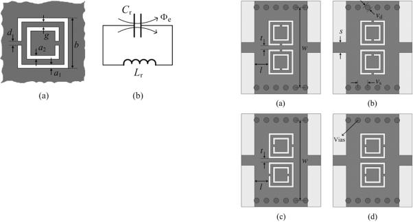
Fig. 12. External factor of the input/output resonator. (Other parameters are
 mm,
mm,  mm, mm, mm, mm,
mm, mm, and mm.)
Fig. 11. (a) Vector magnetic field distribution for low mode. (b) Vector magnetic field distribution for high mode. (c) Resonance frequencies and the coupling coefficient versus the distance 

 between resonators. (Other parameters are
  mm,
mm,  mm, mm, mm, mm,
mm, and mm,)
by simulating a doubly loaded resonator and is calculated by [37] as follows:
(3)
where  is the frequency at which
 reaches its maximum value and


 is the 3-dB bandwidth for which
 is reduced by 3 dB from its maximum value. Usually design curves of the coupling coefficients and external
  factor versus physical dimensions of coupled resonators are established to facilitate the design. Finally, a fine-tuning procedure is often used to optimize the entire filter.
As an illustrative example, a simple two-order filter using two face-to-face aligned SIW-CSRRs is designed following the above procedures. The passband of this filter is located around 5 GHz with a 3.2% fractional bandwidth. By simple circuit synthesis, a coupling matrix is generated in which 


and 


 . The dimensions of the resonator are first determined by simple eigenmode simulation. To determine the internal coupling coefficient, the pair of cascaded resonators is required to be excited with a high external
  factor in order to clearly observe the two resonance frequencies. Here we choose the eigenmode simulation—a more accurate approach to obtain the resonance frequencies. The structure is shown in the inset of Fig. 11(c). Here it is surrounded with solid metallic walls instead of vias in order to expedite simulation. Two eigenmodes around 5 GHz, also known as even and odd modes, are observed. Fig. 11(a) and (b) plots the vector magnetic field distribution of the low and high modes. The coupling coefficient, which is calculated by (2), can be adjusted by changing the distance


Fig. 13. Ideal response and simulated response of the designed two order filter
( mm, mm, mm, mm, mm, |
mm, mm, mm, and mm). |
between the two resonators. Fig. 11(c) presents the relationship between 


 and the coupling coefficient, as well as the eigenmode frequencies.
To determine the external  factor, numerical analysis is carried out on the doubly loaded waveguide resonator shown in the inset of Fig. 12. The coupling is controlled by the waveguide length between the CSRR and input microstrip, which is denoted by
  in this figure. Fig. 12 shows the calculated
 versus
  using (3).
By looking at the above design curves, an optimal physical dimension is obtained. The final filter configuration after some simple tuning is indicated in the inset of Fig. 13. The simulated response is also plotted in Fig. 13, compared with an ideal response from the matrix synthesis. Good agreement is achieved. The unsymmetrical response is attributed to the initial transmission zero of the resonator.
Other resonators can also be used for filter design following similar procedures. The coupling can be controlled in different ways, as shown in the example in Fig. 8. Meanwhile the equivalent circuits discussed earlier can be used to assist the design such as the control of the transmission zeros.

2218 |
IEEE TRANSACTIONS ON MICROWAVE THEORY AND TECHNIQUES, VOL. 57, NO. 9, SEPTEMBER 2009 |
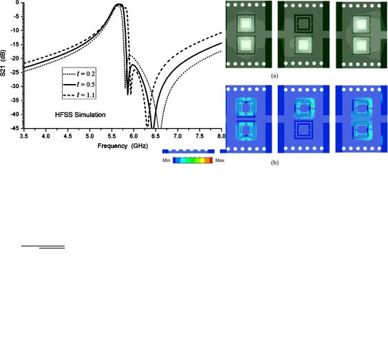
Fig. 14. (a) Photograph of the fabricated first kind of filters. (b) Detailed layout of the three-stage filter. The dimensions of the three-stage filter are
 mm,
mm,  mm, mm, mm, mm,
mm, mm, mm, and 
 mm. CSRR 2 is scaled by a factor of 1.035 on this basis.
IV. FILTER APPLICATION AND EXPERIMENTAL VERIFICATION
In this section, three different types of filters with varied arrangements have been designed and fabricated. They are based on the resonators with CSRRs placed face-to-face, side-by-side reversely oriented [see Fig. 2(a) and (c)], and the proposed new resonators (see Fig. 9), respectively. The Rogers RT/Duroid 5880 substrate with a relative permittivity of 2.2 and a thickness of 0.508 mm was used in all the experiments. All the metallized via arrays exhibit a diameter of 0.8 mm and a center to center spacing around 1.48 mm. These filters were fabricated with the standard PCB process in the High Frequency Center, Electrical Engineering Department, University of California at Los Angeles (UCLA), and they were measured using an Agilent 8510C network analyzer.
A. Filters With Face-to-Face Aligned CSRRs
Fig. 14(a) shows a photograph of the fabricated one-, two-, and three-stage filters using the unit cell shown in Fig. 2(a). Although they are working in a waveguide format, they turn out to be pretty compact. The dimensions of two-stage filter were just shown above. Fig. 14(b) presents the detailed structure and dimensions of the three-stage filter. Note that CSRR 2, as shown in Fig. 14(b), is scaled by a factor of 


 compared with CSRR 1 to adjust its resonance frequency. They are designed following the previously mentioned procedures.
Fig. 15 shows the simulated (dashed line) and measured (solid line) frequency responses of the twoand three-stage filters. The transmission characteristics of the one-stage filter have already been presented in Section II. As expected, twoand three-pole
Fig. 15. Measured and simulated transmission responses of the: (a) two-stage filter and (b) three-stage filter.
filters with transmission zeros located in the upper band are obtained. The three-pole filter has a measured center frequency of 5.05 GHz and a 3-dB bandwidth of 0.33 GHz. Its minimum passband insertion loss is approximately 2.03 dB, which includes the extra loss caused by the subminiature A (SMA) connectors. Its in-band return loss is better than 16.6 dB. Due to the existence of the transmission zeros, this filter exhibits a stopband rejection better than 52 dB, as observed in the measurement. To illustrate the influence of the waveguide highpass band, Fig. 16(a) presents the measured wideband response of the three-pole filter, compared with the simulated frequency response of the SIW, which removes the CSRRs, but shares the same waveguide dimensions. Fig. 16(b) presents the simulated transmission response of the three-pole filter with varied waveguide widths denoted by  . It can easily be seen that by decreasing the waveguide width, the cutoff frequency can be increased, but the passband below the cutoff receives a much smaller influence. Only the coupling is affected.
Fig. 17(a) shows the simulated and measured unwrapped phase response for the oneand two-stage filters. The phase is negative (phase lag) and a decrease in the phase for an additional stage is observed in the passband from 4.75 to 5.2 GHz. This also confirms the forward-wave nature of the propagating passband. Fig. 17(b) shows the measured group delay of the twoand three-stage filters.

DONG et al.: SIW LOADED BY CSSRs AND ITS APPLICATIONS TO MINIATURIZED WAVEGUIDE FILTERS |
2219 |
Fig. 16. (a) Measured wideband response of the three-stage filter compared with the simulated results of the corresponding SIW. (b) Simulated 
 for the three-stage filter with different waveguide widths denoted by .
Fig. 17. (a) Unwrapped 
 phase for oneand two-stage filter obtained from HFSS simulation and measurement. (b) Measured group delay for the threestage filter.
B. Filters With Side-by-Side Reversely Oriented CSRRs
Fig. 18(a) shows a photograph of the fabricated oneand five-stage filters based on the unit cell shown in Fig. 2(c). For the five-stage filter, completely identical CSRRs are employed in order to simplify the optimization. Adjacent unit cells are longitudinally symmetrical. Only the distances between the resonators are tuned to adjust the coupling. The detailed information about the structure of the five-stage filter is presented in Fig. 18(b). In order to better match the 50- microstrip feed-line and the waveguide, a tapered-line transition is used in this particular design.
Fig. 19 shows the simulated (dashed line) and measured (solid line) transmission responses of the filters, whereas the measured group delay for the five-stage filter is also plotted in the inset of Fig. 19(b). Good agreement is achieved. For the onestage filter, we can clearly observe that it is a two-pole filter with two transmission zeros located above the passband. For the five-stage case, a highly selective passband with out-of-band rejection better than 45 dB is observed. The measured in-band return loss is below 19.5 dB, while the measured minimum in-band insertion loss is approximately 5.8 dB. The measured center frequency and 3-dB bandwidth are 5.45 and 0.187 GHz, respectively. The small bandwidth, dielectric loss, conductor loss, and the extra loss from the SMA connectors are all responsible for the high insertion loss. Also bear in mind that this filter actually is a five-stage ten-pole filter. Improved selectivity has been achieved, but with increased insertion loss as a tradeoff.
Fig. 18. (a) Photograph of the fabricated second kind of filters. (b) Detailed layout of the five-stage filter. The dimensions of the five-stage filter are 
mm, mm, mm, |
mm, mm, |
|
|
mm, mm, mm, |
mm, mm, |
|
mm, and mm. |
|
Compared with the group delay of the previous filters shown in Fig. 17(b), the in-band variation of the group delay for this five-stage filter is bigger, which is a result of the smaller bandwidth and the extra transmission zeros.

2220 |
IEEE TRANSACTIONS ON MICROWAVE THEORY AND TECHNIQUES, VOL. 57, NO. 9, SEPTEMBER 2009 |
Fig. 21. (a) Photograph of the fabricated third kind of filters. (b) Detailed layout of the two-stage filter. The dimensions of the two-stage filter are  mm,
mm,
 mm, mm, mm, mm, mm,
mm, mm, and  mm. CSRR 2 is scaled by a factor of 1.052 on this basis.
Fig. 19. Measured and simulated transmission responses of the: (a) one-stage filter and (b) five-stage filter.
Fig. 20. Measured wideband response of the five-stage filter compared with the simulated results of the corresponding SIW. The dispersion diagram of the unit cell is also depicted.
Fig. 20 shows the wideband response of the five-stage filter. It is also compared with the simulated results of the corresponding SIW. The dispersion diagram for the unit cell of the filter is depicted in the inset of the Fig. 20. A narrow forward passband is indicated by the dispersion curve.
C. Filter With Modified CSRRs
Fig. 21(a) shows a photograph of the fabricated filter with one or two unit cells depicted in Fig. 9. The two-stage filter is essentially a four-pole filter and in order to synthesize its passband response, the unit cell is revised as presented in Fig. 18(b). CSRR 2 is scaled by a factor of 


 . The coupling between CSRR 1 and CSRR 2 can be controlled by their distance denoted by
 .
.
Fig. 22 shows the simulated (dashed line) and measured (solid line) transmission responses of the oneand two-stage filters from 2 to 13.5 GHz. For the one-stage filter, two poles with transmission zeros on both sides are obtained. Compared with other filters shown above, a steep transition and a measured stopband rejection better than 40 dB in the lower band are observed. In the upper band, stopband rejection better than
19 dB across a range from 6.5 to  13.5 GHz is achieved. The two-stage filter exhibits a passband with a center frequency at 5.36 GHz and a measured 3-dB bandwidth of 0.62 GHz. A closer look at the in-band transmission given in the inset of Fig. 22(b) shows that the measured minimum in-band insertion loss is approximately 2.63 dB, which includes the loss from the connectors, while the measured in-band return loss for this four-pole filter is below 10.2 dB. It is seen that the attenuation level in the stopband for this filter is further improved. The observed spur in the upper band corresponds to the resonance frequency of the


 mode, and its propagation is suppressed to a level below 30 dB.