диафрагмированные волноводные фильтры / 092c0190-dd51-4f15-a4af-e442289c9d38
.pdf

The resonator structure has central x- and z-planes of symmetry, and essentially central y-plane as well, though the latter one is slightly violated in this implementation due to asymmetric position of the dielectric substrate. These properties are transposed into balanced symmetrical equivalent circuit.
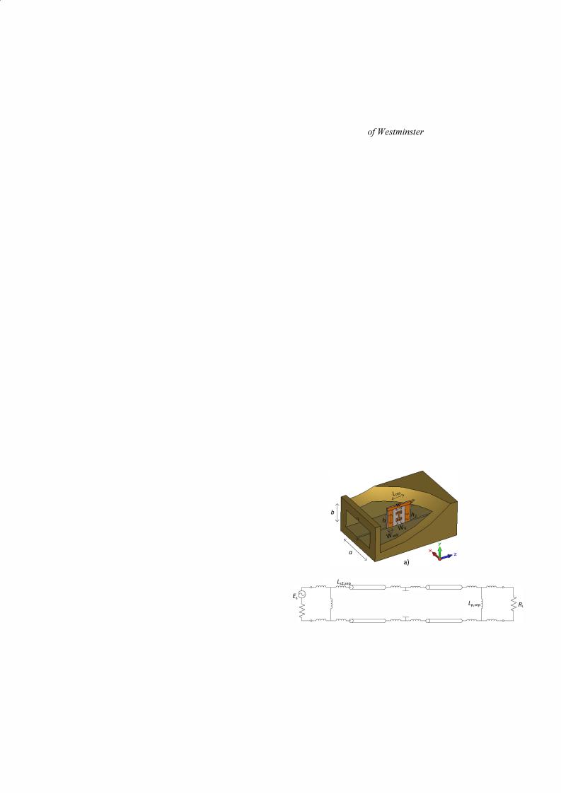
For each resonator discontinuity inside the waveguide, its equivalent 2-port network is extracted from de-embedded center frequency Z-parameters of only that discontinuity independently full wave simulated in the waveguide. Equations Xs1 = Im(zll - zd, Xs2 = Im(z22 - zd and Xp = Im(zd are applied to find Xs1 and Xs2 as serial reactances at ports 1 and 2 respectively and Xp as the parallel reactance of the equivalent T-network. This network is further transfigured into one of equivalent networks in Fig.Ib in a straightforward
manner, |
with |
Ls.ins |
|
and Cs•ins |
satisfying the relation |
|||
Iz |
1 |
2 |
nJLs,ins |
Cs,ins |
' |
where I |
z |
is the frequency of the TZ |
= / |
|
|
|
|||||
produced by an independent I-shaped inset.
The physical length of I-shaped inset is shorter than half a wavelength due to the top and bottom widenings that represent capacitive loadings. Accordingly, the TZ position can be controlled by the inset height as well as by the sizes of loadings. The width of the line representing the loading has been fixed for all the presented designs here to be 0.8 mm. Smaller width has not been used to avoid problems with fabrication sensitivity. Described effect is similar to the one accomplished with adding capacitive loadings to a dipole antenna. Applying image theory across waveguide walls, the I-shaped insets can be transformed into 2D array of dipoles in the transverse z-plane.
The resonant frequency is, expectedly, controlled by the waveguide resonator length. (It is assumed that the waveguide profile is preselected.) The resonator response bandwidth is directed by the amount of coupling between source and load. A more narrowband response can be achieved through wider septa forming immitance inverters, but is produced by a wider I-shaped inset as well.
Sample structures have been designed at X band. Standard WR-90, (a xb)  (22.86 mm xI0.16 mm), rectangular waveguide made of brass (GBr = 15.9 MS/m) with useful frequency band between 8.2 and 12.4 GHz is used. In the top and bottom waveguide walls along one side of the central E-plane are carved 1.5 mm deep and 0.8 mm wide grooves to hold a dielectric slab with etched metallization pattern. The housing itself is longitudinally split in two halves so that the slab can easily be put into the groove in one half and the other
one can afterwards be screwed to the first one. |
|
||
The slab is made out of |
hsub = 0.79 mm thick low |
loss |
|
(tan8 = 0.0009 at 10 GHz) |
Rogers |
RT/duroid 5880 |
high |
frequency laminate having relative permittivity Cr = 2.2 |
[13]. |
||
Electrodeposited copper cladding is |
t = 17!lm thick |
with |
|
Rq = 1.8!lm RMS surface roughness on the dielectric side to result in effective conductivity of GCu.c1ad = 15.4 MS/m.
Propagation characteristics in the waveguide sections between the septa and the insets that are loaded with
off-centered dielectric substrate can be found following the procedure outlined in [14]. In circuit simulation, they are modeled by standard TElO mode sections with the waveguide width increased by 2.73 mm to match the phase constant and characteristic impedance of the actual distorted mode.
The PCB has been fabricated using LPKF ProtoMat C60 [15] circuit board plotter (Fig. 2). However, Rogers RT/duroid 5880 glass microfiber reinforced PTFE composite threaded structure does not appear to be particularly suitable for mechanical milling PCB fabrication, which has to a certain extent negatively affected the measured responses.
Figure 2. Photograph of the two fabricated resonator inserts with the brass waveguide housing.
A.Dominant Mode Resonator
The dominant mode is based on the TElOl rectangular cavity mode. This can be verified by inspecting standing wave patterns in field distribution and by the resonant frequency shifts while altering different resonator dimensions. The electromagnetic field is predictably the strongest in the resonator center region around the inset. Apart from determining the TZ location, the I-shaped inset size affect the transmission pole (TP) location as well since it effectively meanders the EM field inside the resonant cavity. Moreover, the increase in its size more rapidly decreases the resonant frequency than additional cavity length, helping to drastically shrink the resonator size.
In Fig. 3 is given simulated response from CST MICROWAVE STUDIO [16] of a dominant TE101 mode resonator with physical lengths and values of equivalent circuit lumped elements listed in the table I, referring to the dimensions described in Fig. 1. It can be concluded that size reduction of 35% has been achieved compared to the conventional E-plane filter with the same implementation. Between the septum and the inset, the energy is mostly carried by TEnD modes, n = 1, 3, 5, ..., where each higher modes decreases about 10 dB in intensity. When no additional coupling between discontinuities is modeled, TZ frequency is about 6% higher than its real value, whereas TP frequency is only about 1.5% below 10 GHz. The response of the fabricated dominant mode resonator was measured using Agilent E8361A PNA Network Analyzer, and is also presented in Fig. 3 for comparison.


