

диафрагмированные волноводные фильтры / 26aa7fcb-fb46-48d1-a762-c1899443b0a8
.pdfThis article has been accepted for publication in a future issue of this journal, but has not been fully edited. Content may change prior to final publication. Citation information: DOI 10.1109/TIE.2016.2633467, IEEE Transactions on Industrial Electronics
IEEE TRANSACTIONS ON INDUSTRIAL ELECTRONICS
Design and Analysis of EMIT Filter and
Diplexer
Xian Qi Lin, Senior Member, IEEE, Jun Ye Jin, Student Member, IEEE, Jia Wei Yu, Yuan Jiang, Student Member, IEEE, Yong Fan, Member, IEEE and Quan Xue, Fellow, IEEE
Abstract—In this paper, a novel design of E-plane waveguide filter, called electromagnetically induced transparency (EMIT) filter, is proposed. This EMIT filter is implemented by a rectangular ring (RR) on one side of the substrate and two strip lines resonators (SLRs) on the opposite side, which brings in electrically induced transparency (E-IT) and magnetically induced transparency (M-IT) by the electrical and magnetic couplings between the RR and SLRs, respectively. An equivalent circuit is developed further. Properties of high selectivity, low insertion loss, flat group delay and small size of only about 0.2 λg, are realized by this design method. A sample has been fabricated and tested. The measured central frequency is 33.77 GHz with 3-dB fractional bandwidth of 9.4 % and the minimum insertion loss in the passband is 0.5 dB. Using the proposed miniature EMIT filter, a diplexer is further designed with compact sizes and low insertion losses. The measured minimum insertion losses are 0.9 and 0.5 dB in the lower and upper passbands centered at 31.79 and 34.74 GHz with 3-dB relative bandwidths of 7.2% and 8.6%, respectively. Good agreements between the simulated and measured results are obtained both in the EMIT filter and the EMIT diplexer.
Index Terms—Electric and magnetic resonances, electromagnetically induced transparency, EMIT filter, waveguide filter, compact diplexer.
WITH the rapid development of commercial and industrial electronic system, the demand for compact circuit with
Manuscript received January 2, 2016; revised July 22, 2016; accepted November 01, 2016. This work was supported in part by the National Key Basic Research Program of the Ministry of Science and Technology of China (973 Program) under Grant 2014CB339900, in part by the Program for New Century Excellent Talents in University under Grant No. NCET-13-0095, in part by National Natural Science Foundation of China under Grant No.61571084 in part by the Fundamental Research Funds for the Central Universities under Grant No. ZYGX2014J016, in part by the Scientific Research Foundation for the Returned Overseas Chinese Scholars, State Education Ministry.
Xian Qi Lin, Jun Ye Jin, Jia Wei Yu, Yuan Jiang and Yong Fan are with EHF Key Lab of Fundamental Science, School of Electronic Engineering, University of Electronic Science and Technology of China, Chengdu 611731, China. Xian Qi Lin is aslo with the also with the Jiangsu Hengxin Technology Co.,Ltd, Wuxi 214222, China ( E-mail: xqlin@uestc.edu.cn; junyejin2-c@my.cityu.edu.hk).
Jun Ye Jin and Quan Xue are with the State Key Laboratory of Millimeter Waves, Department of Electronic Engineering, City University of Hong Kong, Hong Kong and the Shenzhen Key Lab of MWWC, CityU Shenzhen Research Institute, Shenzhen, China.
higher performances has greatly increased [1]-[3]. Metal- waveguide-based components are widely used in the microwave and millimeter-wave systems, for their robust, low loss, high power capacity and high selectivity coefficient [4, 5]. Conventional waveguide filters are generally implemented by using coupled cavities [6-8], which can realize a high selectivity, but the large size and complex manufactures are inevitable. Then the E-plane filter was proposed as an expedient choice, which is suitable for low-cost and mass production. Since the waveguide E-plane septum filter was introduced by Konishi [9], it has become an important filter structure [10]. For this conventional E-plane waveguide filter, the equivalent circuit consists of impedance inverters and half-wavelength resonators constructed by two adjacent metal septa are alternatively connected. In order to improve the filter performance, the conventional E-plane waveguide filters should cascade more than one resonant cell which leads to large sizes. Recently, some novel waveguide filters have been researched. Compact E-plane filters [11] using metallic septa, C- and I-shaped resonators are investigated based on the conventional coupling theory. SRR-loaded bandpass filters [12] demonstrate the use of the left-handed properties [13] imposed by SRRs to achieve miniaturization of rectangular waveguide filters.
In this paper, a new E-plane waveguide filter design method is proposed, based on the concept of electromagnetically induced transparency (EMIT). The EMIT effect is a coherent control technique to eliminate the opaque effect of a medium in a propagating beam of electromagnetic radiation. It usually leads to an extremely narrow transparency window over a wide absorption band [14]. The effect was demonstrated in optically opaque strontium vapor by K.-J. Boller, A. Imamolu and S. E. Harris [15]. Many applications based on the EMIT effect were reported in quantum scale [16, 17]. More recently, an experiment using a sample of laser-cooled Rb atoms is presented to show that cross-phase modulation schemes continue to benefit from electromagnetically induced transparency (EIT) even as the transparency window is made narrower than the signal bandwidth [18]. Some other studies have also shown that the EMIT effect can be achieved by using non-quantum structures, such as coupled dipole antennas [19], coupled RLC circuits [20], individual Fano resonators with broken symmetry [21], and metamaterial arrays of discrete resonators [22], and an array of resonant antenna pairs placed on a gyromagnetic substrate [23]. In these EMIT structures, two
0278-0046 (c) 2016 IEEE. Personal use is permitted, but republication/redistribution requires IEEE permission. See http://www.ieee.org/publications_standards/publications/rights/index.html for more information.
This article has been accepted for publication in a future issue of this journal, but has not been fully edited. Content may change prior to final publication. Citation information: DOI 10.1109/TIE.2016.2633467, IEEE Transactions on Industrial Electronics
IEEE TRANSACTIONS ON INDUSTRIAL ELECTRONICS
eigen modes named as “bright” mode and “dark” mode, respectively, were induced. Generally, the “bright” mode with low Q-factor exhibits a strong coupling to the radiation field, which produces a large absorption band, i.e. a stopband. The “dark” mode with a higher Q-factor is induced to bring a transparency, i.e. a passband, in the original absorption stopband. In order to widen the transparency window, the conventional approach is to use multiple-layer structures which lead to large size, more insertion loss, and inconvenient application.
In this paper, for widening the transparency window, novel structures are designed to trap two “dark” modes with similar high Q-factors into a “bright” mode with extremely low Q-factor. Based on this concept, a miniature EMIT filter with the properties of high selectivity, low insertion loss and flat group delay is obtained. The theoretical analysis and detail design of such an EMIT filter are presented in section II.
The central frequencies and bandwidth of the designed filter can be designed flexibly. Special designs are presented as well for further better applications in the electronic systems. By using the proposed miniature EMIT filter, a compact diplexer is designed as an example of application in section III. Some conclusions are drawn in section IV.
II. EMIT FILTER DESIGN
In this section, the miniature EMIT filter, a new kind of E-plane bandpass filter, is proposed and designed. As an example, a standard Ka-band waveguide (a=7.112 mm and b=3.556 mm) and the Rogers 5880 substrate (thickness of 0.254 mm and relative permittivity of εr=2.2) are used.
A. Design and analysis of the miniature EMIT filter
In order to introduce a wide stopband, according to the electromagnetically induced transparency theory, a rectangular ring (RR) is constructed in the central E-plane of a standard waveguide, which results in the “bright” mode with a low Q-factor as shown in Fig. 1. This “bright” mode is introduced by the resonance of the rectangular ring, when the waveguide wavelength is equal to the total electrical length of RR. It can be seen that the lower Q (Q < 2) is obtained as increasing the height h1, when the RR resonates at a certain frequency.
After the “bright” mode is designed, two metal strip line resonators (SLRs) are added to the opposite of the RR, i.e. on the bottom surface of the substrate as shown in Fig. 2. Two rectangular waveguide sections with the lengths of lfeed are adopted for feeding and their lengths does not affect the performance of the filter. The “dark” modes are introduced by the electrical and magnetic couplings between the RR and SLRs. These two “dark” modes give birth to the electrical induced transparency (E-IT) and magnetic induced transparency (M-IT). For largest interaction between the two metal strips and the rectangular ring, the distance between the two outer-edges of the two metal strips is designed to be equal to the length of the rectangular ring, i.e. l, and the widths of the metal strips are fixed to be equal to the width of the rectangular ring, i.e. t. The heights of the rectangular ring and the metal strip lines are denoted by h1 and h2, respectively. The electrical and magnetic couplings between the RR and SLRs are
|
0 |
|
|
|
|
|
|
|
(dB) |
-10 |
|
|
|
|
|
|
|
|
|
|
|
|
|
|
|
|
21 |
|
|
|
|
|
|
|
|
S |
-20 |
|
|
|
|
|
|
|
of |
|
|
|
|
|
|
|
|
|
|
|
|
|
|
|
|
|
The amplitude |
-30 |
|
|
|
|
|
|
|
-40 |
|
|
|
|
h1=3.0mm,l=2.0mm |
|||
|
|
|
|
|
|
h1=2.7mm,l=2.7mm |
||
|
-50 |
|
|
|
|
h1=2.0mm,l=3.1mm |
||
|
|
|
|
|
|
|
|
|
|
26 |
28 |
30 |
32 |
34 |
36 |
38 |
40 |
Frequency (GHz)
Fig. 1. The waveguide structure with a metal rectangular ring on the |
|||||||||||||||||||||
substrate and its simulated results (t = 0.15 mm). |
|
|
|
|
|
|
|
|
|
l |
|
|
|
||||||||
|
|
|
|
lfeed |
|
|
|
|
|
|
|
|
|
|
|
h1 |
|||||
|
|
|
|
|
|
|
|
|
|
|
|
|
|
|
|
|
|
|
|||
|
|
|
|
|
|
|
|
|
|
|
|
|
|
|
|
|
|
|
|||
|
lfeed |
l |
|
|
t |
|
|
|
|
|
|
|
|
|
|||||||
|
|
|
|
|
|
|
|
|
|
|
|
|
|||||||||
|
|
|
|
|
|
|
|
|
|
|
|||||||||||
b |
|
|
h1 |
|
|
|
|
|
|
|
|
|
|
||||||||
|
|
|
|
|
|
|
|
|
|
|
|
|
|
|
|
|
|
|
|
||
|
|
|
|
|
|
|
|
|
|
|
|
|
|
|
|
|
|
|
|
||
|
|
|
|
|
|
|
|
|
|
|
|
|
Top |
||||||||
|
|
|
|
|
|
|
|
|
|
|
|
|
|||||||||
|
|
|
|
|
|
|
|
|
|
|
|
|
|
|
|||||||
|
|
h2 |
|
|
|
|
|
|
|
|
|
|
|
|
l |
|
|
|
|||
|
|
|
|
|
|
|
|
|
|
|
|
|
|
|
|
|
|||||
|
|
|
|
|
|
|
|
|
|
|
|
|
|
|
|
|
|||||
|
E |
|
t |
|
|
|
|
|
|
||||||||||||
|
|
|
|
|
|
|
|
|
|
|
|
|
|
|
|
|
|
h2 |
|||
|
a |
|
|
|
|
|
|
|
|
|
|
|
|
|
|
|
|||||
|
|
|
|
|
t |
|
|
|
|
|
|
|
|
|
|||||||
|
|
|
|
|
|
|
|
|
|
|
|
|
|
|
|||||||
|
|
|
|
|
|
|
|
|
|
|
|
|
Bottom |
||||||||
Fig. 2. The proposed EMIT filter, where the value of lfeed negligibly affect the filtering performances.
(dB) |
0 |
|
|
|
|
|
|
-10 |
|
|
|
S11 |
|
|
|
parameters-S |
|
|
|
S21 |
|
|
|
|
|
|
|
|
|
||
|
|
|
|
|
|
|
|
|
-20 |
|
|
|
|
|
|
of |
-30 |
|
|
|
|
|
|
|
|
|
|
|
|
|
|
amplitude |
-40 |
|
|
|
|
|
|
|
|
|
|
|
|
|
|
The |
-50 |
|
|
|
|
|
|
-60 |
|
|
|
|
|
|
|
|
30 |
32 |
34 |
36 |
38 |
40 |
|
|
28 |
Frequency (GHz)
Fig. 3. The simulated results of a proposed EMIT filter (with h1 = h2= 3.2 mm, l = 2 mm and t = 0.15 mm).
determined by sizes of SLRs and RR. Then TZs, E-IT and M-IT are designed. An example with h1 = h2= 3.2 mm, l = 2 mm and t = 0.15 mm is simulated and given in Fig. 3. A wide passband is observed by trapping the two “dark” modes into the “bright” mode. The E-IT and M-IT transparencies together form a flat and wide passband of the designed EMIT filter. Moreover, three transmission zeroes are introduced beside the passband, which effectively improve the selectivity performance of the proposed EMIT filter and out-of-band rejection. The first and second TZs are introduced by the E-IT and M-IT, respectively.
0278-0046 (c) 2016 IEEE. Personal use is permitted, but republication/redistribution requires IEEE permission. See http://www.ieee.org/publications_standards/publications/rights/index.html for more information.

This article has been accepted for publication in a future issue of this journal, but has not been fully edited. Content may change prior to final publication. Citation information: DOI 10.1109/TIE.2016.2633467, IEEE Transactions on Industrial Electronics
IEEE TRANSACTIONS ON INDUSTRIAL ELECTRONICS
|
|
Lc |
Lc |
Zin |
L2 |
Cc L1 |
Cc L2 |
C2 |
C1 |
Zout |
|
|
C2 |
Fig. 4. The equivalent circuit of the proposed EMIT filter.
(dB) |
0 |
|
|
|
|
|
|
|
|
|
|
S11(HFSS) |
|
|
|
-10 |
|
|
|
S21(HFSS) |
|
|
|
parameters-S |
|
|
|
|
|
||
|
|
|
|
S11(Circuit Model) |
|
||
|
|
|
|
|
|
||
|
-20 |
|
|
|
S21(Circuit Model) |
|
|
|
|
|
|
|
|
|
|
of |
-30 |
|
|
|
|
|
|
|
|
|
|
|
|
|
|
amplitude |
-40 |
|
|
|
|
|
|
|
|
|
|
|
|
|
|
The |
-50 |
|
|
|
|
|
|
|
|
|
|
|
|
|
|
|
-60 |
|
|
|
|
|
|
|
28 |
30 |
32 |
34 |
36 |
38 |
40 |
Frequency (GHz)
Fig. 5. The comparisons between the HFSS simulation results and the circuit model analysis results.
|
0 |
|
|
|
|
|
S21(h1 = 3.0 mm) |
|
(dB) |
|
|
|
|
|
|
||
|
|
|
|
|
|
S21(h1 = 3.1 mm) |
||
of S-parameters |
-10 |
|
|
|
|
|
S21(h1 = 3.2 mm) |
|
-20 |
|
|
|
|
|
|
|
|
-30 |
|
|
|
|
|
|
|
|
amplitude |
|
|
|
|
|
|
|
|
-40 |
|
|
|
|
|
|
|
|
The |
|
|
|
|
|
|
|
|
|
-50 |
|
|
|
|
|
|
|
|
26 |
28 |
30 |
32 |
34 |
36 |
38 |
40 |
Frequency (GHz)
Fig. 6. The simulated results of the proposed filter versus h1 (with fixed h2 = 3 mm l = 2 mm and t = 0.15 mm).
The third one for the case with h = 3.2 mm is caused by the self-resonance of SLR.
B. Equivalent circuit analysis of the miniature EMIT filter
The designed EMIT filter can be analyzed by the equivalent circuit method. The rectangular ring is equivalent to a series LC circuit which is composed by L1 and C1 as shown in Fig. 4. Similarly, the two strip lines are represented by two identical series LC circuits which consist of L2 and C2. The capacitance Cc is used to model the E-IT, which is induced by electrical coupling between the RR and SLRs.
Similarly, the inductance Lc is for M-IT, which is brought by magnetic coupling. Larger Cc and Lc mean stronger E-IT and M-IT effect, respectively. By the equivalent circuit, we can analyze the proposed filter theoretically. To demonstrate the effectiveness of the equivalent circuit, the sample (h1 = h2= 3.2 mm= 3.2 mm l = 2 mm and t = 0.15 mm) in Fig. 3 is analyzed
|
0 |
|
|
|
|
|
|
1.0 |
|
|
-10 |
|
|
|
|
|
|
0.9 |
|
|
|
|
|
|
|
|
|
|
|
|
-20 |
|
|
|
|
|
|
0.8 |
|
(dB) |
|
|
|
|
|
|
|
|
|
-30 |
|
|
|
|
|
|
0.7 |
(ns) |
|
|
|
|
|
|
|
|
|||
21 |
|
|
|
|
|
|
0.6 |
||
|
|
|
|
|
|
|
|||
amplitude of S |
|
|
|
|
|
|
|
Group Delay |
|
-40 |
|
|
h=2.8 mm |
|
|
|
0.5 |
||
|
|
|
|
|
|
||||
-50 |
|
|
h=3.0 mm |
|
|
|
0.4 |
||
|
|
h=3.2 mm |
|
|
|
||||
|
|
|
|
|
|
|
|||
-60 |
|
|
|
|
|
|
0.3 |
||
|
|
|
|
|
|
|
|
||
The |
-70 |
|
|
|
|
|
|
0.2 |
|
|
|
|
|
|
|
|
|
||
|
|
|
|
|
|
|
|
|
|
|
-80 |
|
|
|
|
|
|
0.1 |
|
|
|
|
|
|
|
|
|
|
|
|
|
|
|
|
|
|
|
0.0 |
|
|
26 |
28 |
30 |
32 |
34 |
36 |
38 |
40 |
|
Frequency (GHz)
Fig. 7. The simulated results of the proposed filter versus h (h1 = h2 = h with fixed l = 2 mm and t = 0.15 mm).
TABLE I
CHARACTERISTICS OF EMIT FILTER*
h1 = h2 = h (mm) |
f0 (GHz) |
λg/4 (mm) @ f0 |
3-dB bandwidth |
2.8 |
35.36 |
2.64 |
10.2% |
2.9 |
34.55 |
2.74 |
9.8% |
3.0 |
33.12 |
2.94 |
9.5% |
3.1 |
32.13 |
3.09 |
9% |
3.2 |
31.01 |
3.30 |
8.6% |
*Filters with fixed l = 2 mm and t = 0.15 mm.
using this circuit model. The comparisons between the simulation results of HFSS and circuit model are shown in Fig.
5. For Zin = Zout = 1 Ohm, the values of lumped components are as follows: L1 = 0.0026 nH, L2 = 0.00675 nH, Lc = 0.0014 nH,
C1 = 11.31 pF, C2 = 2.787 pF, Cc = 0.24 pF. The agreement between the full wave simulation and circuit model is obtained.
C. EMIT filters with different characteristics
As discussed above, the proposed EMIT filter can be designed and determined by the four parameters of l, t, h1and h2. The lower transmission zero is induced by the E-IT resulting from electrical coupling between the RR and SLRs. Keeping the height of the strip lines with h2 = 3 mm, increasing h1 mainly changes the size of the rectangular ring, the E-IT can be designed and adjusted separately as shown in Fig. 6. The frequencies of lower TZ and maximum E-IT decrease while the M-IT keeps constant. With regard to the equivalent circuit model, L1 increases when h1 increasing. So the same conclusion is obtained. It should be noted that the upper out-of-band rejection level is improved by increasing h1 because of larger
L1.
For easier adjustment, the height of the metal strip is suggested to be equal to the height of the rectangular ring, i.e. h1 = h2 = h, in the following. The simulated |S21| results versus the height parameter of h are shown in Fig. 7. The h can mainly determine the central frequency of the designed EMIT filter. Increasing h can alter both the sizes of metal strip lines and rectangular ring. So the TZs, E-IT and M-IT are all shifted to lower frequencies. It should be mentioned that the third TZs, caused by the self-resonance of SLR, are up to more than 40 GHz for the cases with h = 2.8 mm and h = 3.0 mm.
0278-0046 (c) 2016 IEEE. Personal use is permitted, but republication/redistribution requires IEEE permission. See http://www.ieee.org/publications_standards/publications/rights/index.html for more information.
This article has been accepted for publication in a future issue of this journal, but has not been fully edited. Content may change prior to final publication. Citation information: DOI 10.1109/TIE.2016.2633467, IEEE Transactions on Industrial Electronics
IEEE TRANSACTIONS ON INDUSTRIAL ELECTRONICS
The h plays an important role in determining the central frequency of the designed EMIT filter. The larger h with fixed l = 2 mm and t = 0.15 mm results in a lower central frequency and a slightly narrower bandwidth with a decrement of 1.6 % for h ranging from 2.8 mm to 3.2 mm as listed in Table I. A quarter of waveguide wavelength of the center frequency of filters can be used to estimate the initial value of h as listed in Table I. However, for an accurate design, a simple experienced formula describing the relation between h (in mm) and central frequency f0 (in GHz) of the designed filter can be further developed by fitting numerous simulation data as
h (mm) 5.973 0.0895 f0 , f0 (30GHz,40GHz) . (1)
where f0 is the central frequency. Using this formula, the h can be determined accurately and quickly according to f0. The group delay is of much flatness with a ripple less than 0.07 ns as shown in Fig. 7 as well. The length l of the designed EMIT filter is only 2 mm, which is about 0.2 λg, where λg is the waveguide wavelength of the central frequency of the passband. Such size is much smaller than the previous reported waveguide filters. Besides, if we want to obtain a filter with central frequency below 30 GHz, two mirrored C-shaped can be used to replace the two parallel strip lines.
In applications, the central frequency can be initially designed by h. Then using the t and l to obtain the bandwidth. For example, as shown in Table I, the EMIT filters have central frequencies of 33.12 GHz with a 3dB-bandwidth of 9.5 % and 31.01 GHz with a 3dB-bandwidth of 8.6%, for h = 3.0 mm and h = 3.2 mm respectively. So in order to obtain the filters operating at different central frequencies with similar bandwidths, we can enlarge the bandwidth of the filter with h = 3.2 mm or reduce the bandwidth of the one with h = 3.0 mm. Here, we only discuss how to reduce the bandwidth for the filter with h = 3.0 mm to be about 8.6 %. Two ways can be adopted to adjust the bandwidth. On the one hand, increasing t with fixed l is firstly used. When t = 0.19 mm the bandwidth is reduced to be 8.5 % at a central frequency of 33.07 GHz which is slightly lower than the one (33.12 GHz) with unchanged t as shown in Fig. 8. On the other hand, decreasing l with fixed t can be adopted as well. When l = 1.6 mm the bandwidth is reduced to be 8.6 % at a central frequency of 33.78 GHz which is slightly higher than the one (33.12 GHz) with unchanged l as shown in Fig. 8. So increasing t and decreasing l can reduce the fractional bandwidth and make a frequency shift. By co-designing the three parameters of l, h and t, the desired filter with certain central frequency and bandwidth can be implemented.
For better statement of the bandwidth range, an EMIT filter is designed at the same central frequency with different bandwidths as shown in Fig. 9. The designed EMIT filters operate at 30 GHz with a 3dB-bandwidth of 10.3 % and 3.5 %, respectively. Based on the above simulation investigation and considering the fabrication tolerance, a fractional 3dB-bandwidth between 3% and 11% is suggested for this kind of filter.
Now we conclude the design procedures as follows:
The first step is to determine h using (1) according to the required central frequency.
|
0 |
|
|
|
|
|
|
(dB) |
|
|
|
|
|
Units:all in mm |
|
-10 |
|
|
|
|
|
|
|
parameters-S |
|
|
|
|
|
|
|
-20 |
|
|
|
|
|
|
|
|
|
|
|
|
|
|
|
of |
-30 |
|
|
|
|
|
|
|
|
|
|
|
|
|
|
amplitude |
-40 |
S21(h = 3.2, l = 2.0, t = 0.15) |
|
|
|
|
|
|
|
|
|
|
|||
|
|
|
|
|
|
||
|
-50 |
S21(h = 3.0, l = 2.0, t = 0.15) |
|
|
|
|
|
The |
S21(h = 3.0, l = 2.0, t = 0.19) |
|
|
|
|
||
|
|
|
|
|
|||
-60 |
S21(h = 3.0, l = 1.6, t = 0.15) |
|
|
|
|
||
|
|
|
|
|
|
|
|
|
28 |
30 |
32 |
34 |
36 |
38 |
40 |
Frequency (GHz)
Fig. 8. The EMIT filters with similar bandwidth at different central frequencies.
|
0 |
|
|
|
|
|
|
|
(dB) |
|
|
|
|
@30GHz with a 3dB-bandwidth of 10.3 % |
|||
|
|
|
|
@30GHz with a 3dB-bandwidth of 3.5 % |
|
|||
of S-parameters |
-10 |
|
|
|
|
|||
|
|
|
|
|
|
|
||
-20 |
|
|
|
|
|
|
|
|
-30 |
|
|
|
|
|
|
|
|
amplitude |
|
|
|
|
|
|
|
|
Units:all in mm |
|
|
|
|
|
|
||
-40 |
S21(h = 3.24, l = 2, t = 0.43) |
|
|
|
|
|||
S21(h = 3.28, l = 2.2, t = 0.1) |
|
|
|
|
||||
The |
|
|
|
|
|
|
|
|
|
-50 |
|
|
|
|
|
|
|
|
26 |
28 |
30 |
32 |
34 |
36 |
38 |
40 |
|
|
|
|
Frequency (GHz) |
|
|
|
|
Fig. 9. The EMIT filters operating at 30 GHz with different bandwidth.
Fig. 10. The photographs of the sample EMIT filter, where the lengths of feeding parts negligibly affect the performance of the filtering part.
The second step is to design l and t to obtain the required bandwidth.
D. Experiment of the EMIT filter
A miniature EMIT filter with h = 3 mm, l = 2 mm, t = 0.15 mm is fabricated to demonstrate the above analysis and simulation investigation. The structures are fabricated on the Rogers 5880 substrate with the thickness of 0.254mm and a relative permittivity of εr = 2.2, and then inserted into the central E-plane of the standard waveguide WR-28 with a total length of 20 mm. It should be reminded that the lengths of feeding parts negligibly affect the performance of the filtering
0278-0046 (c) 2016 IEEE. Personal use is permitted, but republication/redistribution requires IEEE permission. See http://www.ieee.org/publications_standards/publications/rights/index.html for more information.

This article has been accepted for publication in a future issue of this journal, but has not been fully edited. Content may change prior to final publication. Citation information: DOI 10.1109/TIE.2016.2633467, IEEE Transactions on Industrial Electronics
IEEE TRANSACTIONS ON INDUSTRIAL ELECTRONICS
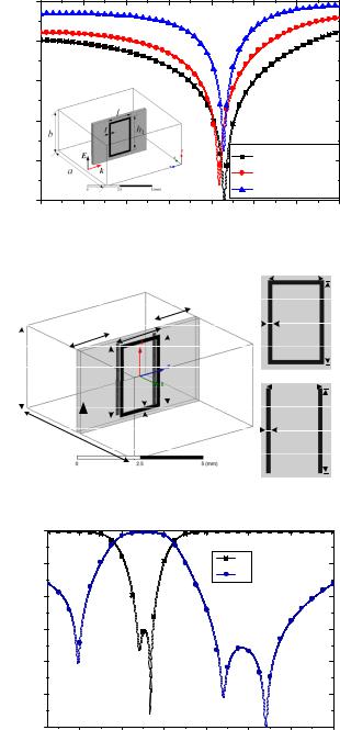
part. Fig. 10 shows the photograph of the fabricated filter. The filter has been tested using the Agilent Technologies A8757D network analyzer and the comparison of simulated and measured results are presented in Fig. 11. TZs occur at both sides of the passband, which significantly contribute to the high selectivity and the sharp attenuation outside the passband. The measured central frequency is 33.77 GHz with a 3-dB fractional bandwidth of 9.4% and the minimum insertion loss in the passband is 0.5 dB. The rejection level in upper stopband is more than 20 dB. Comparing with the simulated one which is at a central frequency is 33.05 GHz with a 3-dB fractional bandwidth of 9.6%, a frequency shift of 0.72 GHz (2.13%) is observed between the simulated and measured results. This is because of the fabrication errors and the material errors.
As a comparison, the transmission coefficient (|S21|) of a conventional E-plane filter with similar central frequency and bandwidth are presented in Fig. 11 as well. Higher selectivity and larger rejection in higher frequency band are obviously achieved in our proposed EMIT filter with the size only about 17.8% of the conventional E-plane filter. We further summarize the performances of different reported E-plane filters in Table II, where we see the most TZs and smallest size of one unit cell are obtained in this work. In [24] and [25], higher rejection levels in out-of-band are presented because higher orders are adopted with much larger sizes. According to the comparison presented in Fig. 11, the EMIT filter with higher orders can obtain a larger rejection level. A certain certification can be found in the next subsection, too. The novel EMIT filter is also more compact than our other previous proposed E-plane filter [26] with a length of less than 0.5 λg and there is no nearby parasitic passband to deteriorate the rejection level in the up-side of the passband.
Besides, the septa presented in [24], [25] and [26] need to be grounded which increases the complexity of assembling. It may be disabled especially for terahertz wave filter design where fissile substrate such as quartz is usually adopted and the septum is too narrow to be fully grounded.
E. Performance of cascaded EMIT cells
As discussed above, the proposed EMIT filter can implement bandpass filter with small sizes. In order to further improve the selectivity and out-of-band rejection, two proposed EMIT cells with anti-position configuration are cascaded as shown in the subset of Fig. 12. The simulated amplitude of S-parameters is illustrated in Fig.12, compared with a single EMIT cell filter. From the comparison, the out-of-band rejection level of two EMIT cells is about doubled. Multiple couplings between two EMIT cells are added and an anther transmission zero is induced in the lower rejection band. The length of cascading filter is 6 mm which is only about 0.6 λg, so the filter is still of much compactness. Finally, in the cascading design, we only adjust the distance between the two cells, and if we slightly optimized the other parameters of the two cells, a better bandpass filter would be obtained.
III. COMPACT DIPLEXER
Diplexer is a very important and critical component in the communication systems. There are many researches focusing on this device [27, 28]. It is usually designed based on a
|
0 |
|
|
|
|
|
|
|
|
(dB) |
-10 |
|
|
|
|
|
|
|
|
of S-parameters |
|
|
|
|
|
|
|
|
|
-20 |
|
|
|
|
|
|
|
|
|
-30 |
|
|
|
|
S11_Sim |
|
|
||
amplitude |
|
|
|
|
|
|
|||
|
|
|
|
|
S21_Sim |
|
|
||
-40 |
|
|
|
|
S11_Mea |
|
|
||
|
|
|
|
|
S21_Mea |
|
|
||
The |
|
|
|
|
|
|
|
||
-50 |
Conventional E-plane filter |
34 |
S21 of conventional filter |
||||||
|
|
28 |
30 |
32 |
|
36 |
38 |
40 |
|
|
|
|
|
Frequency (GHz) |
|
|
|
||
Fig. 11. The comparison of simulated and measured results.
TABLE II
COMPARISON WITH REPORTED RESEARCHES
|
|
|
|
|
|
|
[24] |
[25] |
[26] |
This work |
|
f0(GHz) |
9.45 |
30 |
33.95 |
33.77 |
|
MIL* |
1.6 dB |
0.5 dB |
0.3 dB |
0.5 dB |
|
|
|
|
|
|
|
FBW* |
4.5 % |
10 % |
9.7 % |
9.4 % |
|
|
|
|
|
|
|
TZ* |
1 in up side |
none |
2 in both |
1 in down, |
|
side |
2 in up side |
||||
|
|
|
|||
Orders |
3 |
5 |
1 |
1 (dual-mode) |
|
Size(mm) |
58.4>1.3λg |
39.98>2.5λg |
5<0.5λg |
2<0.2λg |
* MIT, TZ and FBW denote the Minimum Insertion Loss, Transmission zero and 3-dB Fractional Bandwidth.
|
0 |
|
|
|
|
|
|
|
(dB) |
-20 |
|
|
|
|
|
|
|
|
|
|
|
|
|
|
|
|
S-parameters |
-40 |
|
|
|
|
|
|
|
-60 |
|
d |
|
S11_two |
|
|
|
|
|
|
|
|
S21_two |
|
|
|
|
|
|
b |
|
|
|
|
|
|
|
|
|
|
S11_single |
|
|
|
|
|
-80 |
|
|
|
|
|
|
|
|
a |
|
|
S21_single |
|
|
|
|
|
|
|
|
|
|
|
||
|
26 |
28 |
30 |
32 |
34 |
36 |
38 |
40 |
|
|
|
|
Frequency (GHz) |
|
|
|
|
Fig. 12. Simulated results of filters with single EMIT cell and two cascaded EMIT cells (with d = 2 mm, t = 0.2 mm, h = 3 mm and l = 2 mm).
waveguide or metal cavity with better performances in lower loss and higher power capacity [29, 30]. However, the design suffers disadvantages such as bulky, costly, and difficult to fabricate. In particular, the passive components are required to be easily integrated or assembled with active circuits in a highly integrated system. In this section, we plan to utilize the proposed EMIT filter to investigate a compact diplexer.
A. Design and analysis of the compact diplexer
0278-0046 (c) 2016 IEEE. Personal use is permitted, but republication/redistribution requires IEEE permission. See http://www.ieee.org/publications_standards/publications/rights/index.html for more information.

This article has been accepted for publication in a future issue of this journal, but has not been fully edited. Content may change prior to final publication. Citation information: DOI 10.1109/TIE.2016.2633467, IEEE Transactions on Industrial Electronics
IEEE TRANSACTIONS ON INDUSTRIAL ELECTRONICS
|
|
|
|
|
|
l1 |
|
l2 |
|
|
|
|
|
|
|
t1 |
|
t2 |
P3 |
|
|
|
|
b |
P2 h1 |
d2 |
h2 |
||
|
|
|
|
|
|
d1 |
|
|
|
|
|
|
|
|
|
l1 |
Top |
l2 |
|
b |
|
|
|
a |
t1 |
|
|
t2 |
|
|
|
|
|
|
|
h1 |
h2 P3 |
||
|
|
|
|
|
P2 |
|
|||
|
a |
|
|
|
|
|
|
|
|
|
|
|
|
|
|
Bottom |
|
|
|
|
|
(a) |
|
|
|
|
(b) |
|
|
|
0 |
|
|
|
Filter2 |
|
|
|
|
|
|
|
|
Filter1 |
|
|
|
||
(dB) |
-10 |
|
|
|
|
|
|
|
|
-20 |
|
|
|
|
|
|
|
|
|
21 |
|
|
|
|
|
|
|
|
|
of S |
|
|
|
|
|
|
|
|
|
The amplitude |
-30 |
|
|
|
|
|
|
|
|
-40 |
|
|
|
|
|
|
|
|
|
-50 |
h1=3.2 mm,t1=0.15 mm |
|
|
|
|
|
|||
|
|
|
|
|
|
||||
|
|
h2=2.9 mm,t2=0.2 mm |
|
|
|
|
|
||
|
-60 |
|
|
|
|
|
|
|
|
|
26 |
28 |
30 |
32 |
34 |
|
36 |
38 |
40 |
Frequency (GHz)
(c)
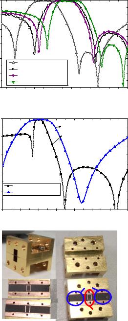
Fig. 13. Configurations of the compact diplexer: (a) simulation mode,
(b) the metal structures of the substrate and (c) the scheme of the diplexer and simulated results of Filter1 and Filter2 (with l1= l2=1.8mm).
The conventional H-plane T-junction is adopted in the compact diplexer design for easy fabrication, as shown in Fig. 13. Two proposed EMIT filters (denoted by Filter1 and Filter2) with different sizes are employed to the two symmetric alarms of the T-junction as two passes for different operating bands. The scheme is also given in the subfigure in Fig. 13(c). In the design procedures, two steps are taken as follows:
First, the sizes of the two EMIT filters are determined according to the central frequencies and bandwidths of the two channels. Here, Filter1 and Filter2 with the different sizes shown in Fig. 13(c)are chosen to realize the diplexer and the simulated results of these two filters are given as well. In order to achieve high isolation between two channels, the passband of lower channel is designed to locate around the transmission zero of the upper channel by tuning the parameters of h1, l1 and t1. Meanwhile, passband of the upper channel is designed to locate around the transmission zero of the lower channel by tuning the parameters of h2, l2 and t2.
Second, the distancesd1 and d2 are adjusted to optimize the diplexer performance. By adjusting d2, it is possible that the input impedance looking from the central of the T-junction into the upper channel arm (Filter2) is equivalent to an open circuit to the T-junction, and the signal input from the waveport 1 (P1) is transmitted into the waveport 2 (P2). Vice versa, i.e. the upper channel operates normally while the lower channel (Filter1) equals to an open circuit by adjustingd1. If needed, fine tuning the sizes of two filters can be added to obtain better diplex performances especial when high-order EMIT filters are adopted.
Fig. 14. The photographs of the diplexer.
|
0 |
|
|
|
|
|
|
|
|
-10 |
|
|
|
|
|
|
|
results |
-20 |
|
|
|
|
|
|
|
|
|
|
|
|
|
|
|
|
Simulated |
-30 |
|
|
|
|
|
|
|
|
|
|
|
|
|
|S11| _Sim. |
|
|
|
-40 |
|
|
|
|
|
|S21| _Sim. |
|
|
|
|
|
|
|
|
|S31| _Sim. |
|
|
-50 |
|
|
|
|
|
|S23| _Sim. |
|
|
28 |
30 |
32 |
34 |
36 |
38 |
40 |
|
|
|
|||||||
|
|
|
|
Frequency (GHz) |
|
|
|
|
|
|
|
|
(a) |
|
|
|
|
0 |
|
|
|
|
|
|
results |
-10 |
|
|
|
|
|
|
-20 |
|
|
|
|
|
|
|
Measured |
|
|
|
|
|
|
|
-30 |
|
|S11|_Mea. |
|
|
|
||
|
|
|
|
|
|
||
|
|
|
|S21|_Mea. |
|
|
|
|
|
-40 |
|
|S31|_Mea. |
|
|
|
|
|
|
|
|S23|_Mea. |
|
|
|
|
|
28 |
30 |
32 |
34 |
36 |
38 |
40 |
|
|
|
Frequency (GHz) |
|
|
|
|
(b)
Fig. 15. The simulated and measured results of the compact diplexer (l1= 1.8mm, h1=3.2mm, t1=0.15mm, l2= 1.8mm, h2=2.9mm, t2=0.2mm, d1 =2.7mm, d2=2.6mm). (a) the simulated responses. (b) the measured responses.
B. Experiment of the compact diplexer
According to the design procedures presented above and combining the use of full-wave simulation software, the proposed compact diplexer is finally designed. After fine tuning, the parameters are determined, i.e. d1= 2.7 mm and d2= 2.6 mm respectively. This compact diplexer is finally fabricated and its photographs are shown in Fig.14. The total length of the compact diplexer is only 8.9 mm which is about 0.9 λg. However, in order to easily assemble and test, two sections of blank substrate with length of 10.5mm are added at the input and output ports. So the total length of the fabricated diplexer is 30 mm.
0278-0046 (c) 2016 IEEE. Personal use is permitted, but republication/redistribution requires IEEE permission. See http://www.ieee.org/publications_standards/publications/rights/index.html for more information.
This article has been accepted for publication in a future issue of this journal, but has not been fully edited. Content may change prior to final publication. Citation information: DOI 10.1109/TIE.2016.2633467, IEEE Transactions on Industrial Electronics
IEEE TRANSACTIONS ON INDUSTRIAL ELECTRONICS
The simulated and measured results are illustrated in Fig. 15. The measured minimum insertion losses are 0.9 and 0.5dB in the lower and upper passbands centered at 31.79 GHz and 34.74 GHz with 3-dB fractional bandwidths of 7.2% and 8.6% respectively. The isolation between the two channels is more than 15 dB in the operating frequency band. This type of diplexer is very suitable for the applications where compact sizes, low insertion losses and wide passbands are required. We would like to mention that the isolation can be further improved by cascading more EMIT cells.
IV. CONCLUSION
In this paper, a miniature waveguide filter, called EMIT filter is designed, fabricated and tested. The miniature EMIT filter is constructed by inserting a substrate into the central E-plane of a standard rectangular waveguide. E-IT and M-IT are induced by the electrical and magnetic couplings between the RR and SLRs. This kind of EMIT filter has the properties of high selectivity, low insertion loss and flat group delay. The length of fabricated EMIT filter is only about 0.2 λg. Using the proposed EMIT filter, a compact diplexer with a length of about 0.9 λg is designed and tested, achieving a very low insertion loss about 0.5 dB and an isolation more than 15 dB. Since the size of the filter is very small, it is easy to improve the isolation by adding more EMIT cells without significantly increase the sizes of the components. No grounded structures are required so the assembling error is decreased especially for those commercial and industrial electronic systems with extremely high working-frequencies.
REFERENCES
[1]H. L. Zhang, B. J. Hu, and X. Y. Zhang, “Compact equal and unequal dualfrequency power dividers based on composite right-/left-handed transmission lines,” IEEE Trans. Ind. Electron., vol. 59, no. 9, pp. 3464–3472, Sep. 2012.
[2]P.C. Loh, L. Zhang, and F. Gao, “Compact Integrated energy systems for distributed generation,” IEEE Trans. Ind. Electron., vol. 60, no. 4, pp. 1492–1502, Apr. 2013.
[3]Q. S. Xu, “Design and Development of a compact flexure-based XY precision positioning system with centimeter range,” IEEE Trans. Ind. Electron., vol. 61, no. 2, pp. 893–903, Feb. 2014.
[4]S.S. Stuchly, M. A. Rzepecka, M. A. K. Hamid, “A microwave open-ended cavity as a void fraction monitor for organic coolants,” IEEE Trans. Ind. Electron. and Contr. Instru., vol. 61, no. 2, pp. 893–903, Feb. 1974.
[5]R. Leewe, M. Moallem, K. Fong, “Control of RF cavity resonance frequency using reflected power measurements,” in 39th IEEE Ind. Electron. Annual Conf., vol. 1, no. 1, Nov. 2013, pp. 3428–3432,.
[6]A. E. Williams, “A four-cavity elliptic waveguide filter,” IEEE Trans. Microw. Theory Techn., vol. 18, no. 12, pp. 1109-1114, Dec. 1970.
[7]P. Soto, E. Tarín, V. E. Boria, C. Vicente, J. Gil, and B. Gimeno, “Accurate synthesis and design of wideband and inhomogeneous inductive waveguide filters,” IEEE Trans. Microw. Theory Techn., vol. 58, no. 8, pp. 2220-2230, 2010.
[8]K. Song, F. Zhang, S. Hu, and Y. Fan, “Ku-band 200-W pulsed power amplifier based on waveguide spatially power-combining technique for industrial applications,” IEEE Trans. Ind. Electron., vol. 61, no. 2, pp. 893–903, Feb. 2014.
[9]Y. Konishi, and K. Uenakada, “The design of a bandpass filter with inductive strip--planar circuit mounted in waveguide,” IEEE Trans. Microw. Theory Techn., vol. 22, no. 10, pp. 869-873, Oct. 1974.
[10]S. Yi-Chi, and T. Itoh, “E-Plane Filters with Finite-Thickness Septa,” IEEE Trans. Microw. Theory Tech., vol. 31, no. 12, pp. 1009-1013, Dec. 1983.
[11]S. Niranchanan, D. Budimir, and F. Kamal, "Waveguide filters based on conventional and complementary split ring resonators for microwave and millimetre-wave wireless applications." In IEEE Int. Symp. Antennas Propag., 2007, pp. 461-464,
[12]R. Marques, J. Martel, F. Mesa, and F. Medina, “Left-handed-media simulation and transmission of EM waves in subwavelength split-ring-resonator-loaded metallic waveguides,” Phys. Rev. Lett., vol. 89, no. 18, pp. 183901-4, Oct. 2002.
[13]T. Decoopman, A. Marteau, E. Lheurette, O. Vanbésien, and D. Lippens, “Left-handed electromagnetic properties of split-ring resonator and wire loaded transmission line in a fin-line technology,” IEEE Trans. Microw. Theory Techn., vol. 54, no. 4, pp. 1451-1457, Apr. 2006.
[14]R. D. Kekatpure, E. S. Barnard, W. Cai, and M. L. Brongersma, “Phase-coupled plasmon-induced transparency,” Phys. Rev. Lett., vol. 104, no. 24, pp. 243902-4, Jun. 2010.
[15]K.-J. Boller, A. Imamolu, and S. E. Harris, “Observation of electromagnetically induced transparency,” Phys. Rev. Lett., vol. 66, no. 20, pp. 2593-6, May 1991.
[16]J. Marangos, “Electromagnetically induced transparency,” J. Modern Optics, vol. 45, no. 3, pp. 471-503, Mar. 1998.
[17]T. Philippe, Z. Lei, Z. Rongkuo, J. Aditya, K. Thomas, and S. C. M, “Electromagnetically induced transparency and absorption in metamaterials: the radiating two-oscillator model and its experimental confirmation,” Phys. Rev. Lett., vol. 109, no. 18, pp. 187401-4, Oct. 2012.
[18]G. Dmochowski, A. Feizpour, M. Hallaji, C. Zhuang, A. Hayat, and A. M. Steinberg, “Experimental demonstration of the effectiveness of electromagnetically induced transparency for enhancing cross-phase modulation in the short-pulse regime”, Phys. Rev. Lett., vol. 111, no. 17,
pp.3002, Apr. 2016.
[19]B. A. Munk and R. J. Luebbers, "Reflection Properties of Two-Layer Dipole Arrays," IEEE Trans. Antenna and Propag., vol. 22, no. 6, pp. 766-773, Jun. 1974.
[20]C. G. Alzar, M. Martinez, and P. Nussenzveig, “Classical analog of electromagnetically induced transparency,” Am. J. Phys., vol. 70, no. 1,
pp.37-41, 2002.
[21]R. Singh, I. A. Al-Naib, Y. Yang, D. R. Chowdhury, W. Cao, C. Rockstuhl, T. Ozaki, R. Morandotti, and W. Zhang, “Observing metamaterial induced transparency in individual Fano resonators with broken symmetry,” Appl. Phys. Lett., vol. 99, no. 20, pp. 201107, Nov. 2011.
[22]S. D. Jenkins and J. Ruostekoski, “Metamaterial Transparency Induced by Cooperative Electromagnetic Interactions” , Phys. Rev. Lett., vol. 111, no. 14, pp. 7401, Sep. 2013.
[23]S. H. Mousavi, A. B. Khanikaev, J. Allen, M. Allen and G. Shvets, “Gyromagnetically induced transparency of metasurfaces,” Phys. Rev. Lett., vol. 112, no. 11, pp. 7402, Mar. 2014.
[24]D. Budimir, O. Glubokov, and M. Potrebić, “Waveguide filters using T-shaped resonators,” Electronics Lett., vol. 47, no. 1, pp. 38, Jan. 2011.
[25]Z. Xu, J. Guo, C. Qian, and W. Dou, “Broad-Band E-plane Filters With Improved Stop-Band Performance,” IEEE Microw. Wireless Compon. Lett., vol. 21, no. 7, pp. 350-352, Jul. 2011.
[26]J. Y. Jin, X. Q. Lin, Y. Jiang, L. Wang, and Y. Fan, “A novel E-plane substrate inserted bandpass filter with high selectivity and compact size,”
Int. J. RF Microw. Comput.-Aided Eng., vol. 24, no. 4, pp. 451-456, Jul. 2014.
[27]O. Mirabella, M. Brischetto, A. Raucea, “Performance evaluation by petrinets of a full duplex wireless link for an industrial backbone,” in 34th IEEE Ind. Electron. Annual Conf., Nov. 2008, pp. 1520–1526.
[28]K. Thirupathaiah, B. Iyer, N. P. Pathak and V. Rastogi, “Concurrent Dualband Diplexer for Nanoscale Wireless Links,” IEEE Photonics Techn. Lett., vol. 26, no. 18, pp. 1832-1835, Jul. 2014.
[29]F. M. Vanin, D. Schmitt, and R. Levy, “Dimensional synthesis for wide-band waveguide filters and diplexers,” IEEE Trans. Microw. Theory Tech., vol. 52, no. 11, pp. 2488-2495, 2004.
[30]C. Chen, L. Chen, P. Zhao, “A waveguide diplexer based on E-plane T-junction,” in 15th Int. Conf. Electronic Packaging Techn. (ICEPT), Aug. 2014, pp. 1390-1391.
0278-0046 (c) 2016 IEEE. Personal use is permitted, but republication/redistribution requires IEEE permission. See http://www.ieee.org/publications_standards/publications/rights/index.html for more information.

This article has been accepted for publication in a future issue of this journal, but has not been fully edited. Content may change prior to final publication. Citation information: DOI 10.1109/TIE.2016.2633467, IEEE Transactions on Industrial Electronics
IEEE TRANSACTIONS ON INDUSTRIAL ELECTRONICS
Xian Qi Lin (M'08, SM'15) was born in Zhejiang Province, China, on July 9, 1980. He received the B.S. degree in electronic engineering from UESTC (University of Electronic Science and Technology of China), Chengdu, China, in 2003, and Ph.D. degree in electromagnetic and microwave technology from Southeast University, Nanjing, China, in 2008. He joined the Department of Microwave Engineering at UESTC in August 2008, and has become an Associate Professor and a doctoral supervisor
since July 2009 and December 2011, respectively. From September 2011 to September 2012, He was a post-doc researcher in the Department of Electromagnetic Engineering at Royal Institute of Technology (KTH), Stockholm, Sweden. He is currently a Full Professor in UESTC.
He has authored over 10 patents, over 40 scientific journal papers, and has presented over 20 conference papers. His research interests include microwave/millimeter-wave circuits, metamaterials and antennas.
Jun Ye Jin (S’11) was born in Inner Mongolia, China. She received the B.S. and M.S. degree in Electromagnetics and Microwave Technology from the University of Electronic Science and Technology of China (UESTC), Chengdu, China, in 2011 and 2014. She is currently working toward Ph.D. degree at the State Key Laboratory of Millimeter Waves, Department of Electronic Engineering, City University of Hong Kong, Hong Kong and Shenzhen Research Institute, City
University of Hong Kong, Shenzhen, China. Her research interests include microwave or millimeter-wave circuits and systems and RFIC design.
Jia Wei Yu was born in Sichuan Province, China, on March, 1991. He received the B.S. degree in electromagnetic and wireless technology from UESTC (University of Electronic Science and Technology of China), Chengdu, China, in 2012. He is currently pursuing the Ph.D. degree in electromagnetic and microwave technology at UESTC.
Yuan Jiang (S’12) was born in Jiangsu Provence, China. He received the B.S. and M.S. degrees in Electronic Engineering from the University of Electronic Science and Technology of China (UESTC), Chengdu, China, in 2010 and 2012, respectively. Since 2012, he is working toward the Ph.D. degree at UESTC.
His research interests include microwave passive components, active components and antennas, especially focus on reconfigurable/tunable technologies.
Yong Fan (M’05) received the B.E. degree from Nanjing University of Science and Technology, Nanjing, Jiangsu, China, in 1985 and the M.S. degree from University of Electronic Science and Technology of China, Chengdu, Sichuan, China, in 1992.
He is now with the School of Electronic Engineering, University of Electronic Science and Technology of China, where he is currently a full Professor. His current research interests include electromagnetic theory, millimeter-wave
technology, communication and system. He has authored and co-authored over 130 papers.
Quan Xue (M’02–SM’04–F’11) received the B.S., M.S., and Ph.D. degrees in electronic engineering from the University of Electronic Science and Technology of China (UESTC), Chengdu, China, in 1988, 1991, and 1993, respectively. In 1993, he joined the UESTC, as a Lecturer. He became a Professor in 1997. From October 1997 to October 1998, he was a Research Fellow with the Chinese University of Hong Kong. In 1999, he joined the City University of Hong Kong where he is currently a
Chair Professor of Microwave Engineering. He is now the Director of ICTC, and the Deputy Director of the State Key Lab of Millimeter Waves (Hong Kong).
He has authored or co-authored over 300 journal papers and over 120 conference papers. He is co-inventors of 5 granted Chinese patents and 12 granted US patents. His research interests include microwave/millimeter-wave/THz passive components, active components, antenna, MMIC, and RFIC etc.
0278-0046 (c) 2016 IEEE. Personal use is permitted, but republication/redistribution requires IEEE permission. See http://www.ieee.org/publications_standards/publications/rights/index.html for more information.