

диафрагмированные волноводные фильтры / 22d45abe-5c5c-4bb6-b5c1-d25e110c1bf0
.pdf2968 |
IEEE TRANSACTIONS ON MICROWAVE THEORY AND TECHNIQUES, VOL. 53, NO. 9, SEPTEMBER 2005 |
Compact Super-Wide Bandpass Substrate
Integrated Waveguide (SIW) Filters
Zhang-Cheng Hao, Wei Hong, Member, IEEE, Ji-Xin Chen, Xiao-Ping Chen, and Ke Wu, Fellow, IEEE
Abstract—It is known that the substrate integrated waveguide (SIW) features high-pass characteristics of the conventional waveguide, and a periodic structure (PS) generally presents bandstop characteristics. Therefore, a super-wide-band bandpass characteristic should be realized by combining some sort of PS into the SIW. In this paper, three types of compact SIW-PS wide-band bandpass filters are proposed and investigated with simulation and experiment. Performances of a super-wide bandpass, for instance, 8.5–16.5 GHz in this case study, with low insertion loss and sharp out-of-band characteristics are observed from both simulated and measured results.
Index Terms—Bandpass filter, coplanar waveguide (CPW), defect ground structure (DGS), electromagnetic bandgap (EBG), substrate integrated waveguide (SIW).
I. INTRODUCTION
IN THE last several years, various types of periodic structures such as electromagnetic bandgap structures (EBGs) and defect ground structures (DGSs) etc. [1]–[14] have been a popular research topic, and they have generated significant interests in applications for microwave and millimeter-wave circuits design. A planar periodic structure called high-impedance- ground structure, for example, has been proposed and used to improve antenna performances [2], and a compact EBG structure named the uniplanar compact EBG (UC-EBG) was realized with periodic metal pads etched on ground plane connected by narrow lines to form a distributed LC network [1], [6], [7]. Some planar periodic structures such as compact coplanar waveguide (CPW) periodic structures have been used to realize highperformance filters or to reduce harmonic effects in power amplifiers and to suppress leakage in CB-CPWs [4], [15]–[17]. These applications become possible because the periodic structures exhibit excellent bandstop characteristics when patterned on a microstrip ground plane. In addition, slow-wave characteristics manifesting along the periodic structures can be exploited
to reduce the microstrip component size [4].
Recently, a convenient and interesting planar scheme called the substrate integrated waveguide (SIW) has already attracted
Manuscript received December 20, 2004; revised April 18, 2005. This work was supported in part by the National High Technology Research Plan of China (863 Plan) under Grant 2002AA123031, by the National Science Foundation of China under Grant 60390540, and by the China Postdoctoral Science Foundation under Grant 2004035654
Z.-C. Hao, W. Hong, J.-X. Chen, and X.-P. Chen are with the State Key Laboratory of Millimeter Waves, Department of Radio Engineering, Southeast University, Nanjing 210096, China (e-mail: zchao@emfield.org; weihong@ seu.edu.cn).
K. Wu is with the Poly-Grames Research Center, Department of Electrical Engineering, Ecole Polytechnique, University of Montreal, Montreal, QC, Canada H3V 1A2 (e-mail: wuke@grmes.polymtl.ca).
Digital Object Identifier 10.1109/TMTT.2005.854232
much interest in the design of microwave and millimeter-wave integrated circuits [19]–[43]. The SIW is synthesized in dielectric substrate with linear arrays of metallic vias, and it can also be treated as a periodic structure [10], [43]. The field distribution in an SIW is similar to that in a conventional rectangular waveguide, thus SIW components inherit the advantages of the rectangular waveguide such as high  factor, low insertion loss, and high-power capability [27]–[43]. This scheme is also feasible for designing ridged waveguides in low—temperature co-fired ceramic (LTCC) [20], [22], [24]–[27]. Similar structures realized in the LTCC process are also known as laminated waveguide and post-wall waveguide [20], [21], [38]–[40]. The SIW components such as filters, multiplexers, antennas, and power dividers have been studied by researchers in [24]–[43]. Such tremendous research progresses show that the SIW can be deployed in the design of microwave and millimeter-wave integrated circuits with very promising performances.
Since the SIW has a cutoff frequency characteristic and a periodic structure generally has a bandstop behavior, compact wide-band filters can thus be obtained by integrating the SIW with a periodic structure. This study proposes and examines different integration techniques of SIW with UC-EBG, UC-DGS, and CPW periodic structures, respectively, and wide-band filters with low insertion loss are obtained. These filters present a much wider bandwidth than the conventional SIW filter does. On the other hand, the SIW and periodic structures such as UC-EBG, DGS, and CPWs are highly integrated together, and the resulting filters therefore have a much smaller size than the conventional SIW filter, whose size is comparable to its operating guided wavelength (

 or
or 

 ) [24]–[27], [35]. Further, such filters exhibit low insertion loss and good selectivity due to the high
  factor of SIW and the low loss characteristics of periodic structures (UC-EBG and CPW) [1], [4], [19].
In this paper, design considerations for these wide-band filters are introduced in Section II, where geometrics of these filters are illustrated, and simulation results are presented in Section III. In Section IV, experiments are provided and discussed with measured results, followed by conclusions in Section V.
II.DESIGN CONSIDERATIONS
A.SIW and UC Photonic-Bandgap (UC-EBG) Structure
Fig. 1 shows the SIW structure and the UC-EBG cell with their geometric parameters. In Fig. 1(a), the SIW is made of two linear metallic via arrays in dielectric substrate with a height of  . These metallic via arrays confine the electromagnetic fields inside the SIW. The SIW has a width of


 , and the metallic
0018-9480/$20.00 © 2005 IEEE

HAO et al.: COMPACT SUPER-WIDE BANDPASS SIW FILTERS |
2969 |
Fig. 1. Configurations for (a) the SIW and (b) the UC-EBG cell with their geometric parameters.
vias have a diameter of 


 and the space between the adjacent vias is


 . A relationship between the conventional rectangular waveguide and the SIW can be used to initially determine the geometric parameters [34], and it can be described as follows:
(1)
where  is a normalized coefficient,

 is the width of the corresponding rectangular waveguide, and

 and
and  are defined as
Fig. 2. Configuration for SIW-EBG filter. (a) Front view. (b) Back view.
(2)
Then, the cutoff frequency for the SIW can be defined as 


 in which
  is the light velocity in vacuum.
In Fig. 1(b), the geometric parameters for UC-EBG cell are depicted. When the UC-EBG cells are connected periodically, this two-dimensional (2-D) EBG structure can in fact be considered as a periodically loaded structure with gap capacitances and reactances provided by connecting branches [3]. In this way, a transmission-line model that is periodically loaded with a lumped impedance  consisting of
  (
( is the reactance of the resonator for a UC-EBG cell) in parallel with
  (
( represents the coupling capacitor between neighboring resonators) with a period of
  can be used to model this UC-EBG structure, so propagation constant
  and bandgap can be determined by [3]
(3)
where  is the characteristic impedance and
  is the phase constant for the unloaded structure. For a periodic structure, the
propagation constant within the stopband is zero or 


 [1], [3]. Within the passband, the propagation constant
  can be obtained using (3) at different frequencies.
Using (1)–(3), we can design the SIW and UC-EBG analytically. It is noted that, since the inductive and capacitive values for any periodic structure are not entirely independent because of coupling effects [4], [18], we can only make use of the parameters obtained from (1)–(3) as initial values for the design of filters, and a complete full-wave analysis is required for the subsequent tuning process. In this design, we adjust those parameters for SIW and UC-EBG with the aid of the commercially available Ansoft High Frequency Structure Simulator (HFSS) software.
B. SIW-EBG Filter
Fig. 2 shows the configuration for the SIW-EBG filter. The SIW is synthesized by the metallic vias which are separately placed at the center of the UC-EBG cells. As shown in Fig. 2(b), in the central UC-EBG cell array, there are no metallic vias,
2970 |
IEEE TRANSACTIONS ON MICROWAVE THEORY AND TECHNIQUES, VOL. 53, NO. 9, SEPTEMBER 2005 |
Fig. 4. Configuration for the proposed SIW-CPW filter. (a) Front view.
(b) Back view.
Fig. 3. Configuration for SIW-DGS filter. (a) Front view. (b) Back view.
and the electromagnetic wave can pass through it without reflection caused by the metallic vias in the passband. Then, the SIW width is twice the width of the UC-EBG cell. The space between UC-EBG cells is denoted by 


 .
.
Since the filter operates over a wide frequency range in this case, it is difficult to design a wide-band SIW-microstrip transition for its input and output. For measurement purposes or possible interconnects with other components, two short lengths of hard ground plane have been used as parts of the filter, and two 50- microstrips shown in Fig. 2(a) are directly connected with the up-cover of SIW for the input and output. The space between the first UC-EBG cells to the hard ground is
 .
.
Once the geometric parameters of UC-EBG cells are chosen in the design, the width of the SIW and the space between metallic vias that are critical for the SIW are then determined. The parameter related to the diameter of the metallic via can be used to tune the cutoff frequency.
It is found that the metallic cover should not be overlapped with the hard ground plane in this structure. This is because the electromagnetic field will be strongly coupled and a large capacitor will be introduced.
C. SIW-DGS Filter
As shown in Fig. 2, the geometric parameters for the SIW-EBG filter are mainly limited by the UC-EBG cells. Therefore, it is not convenient to design the SIW filter in this way. We can replace the lateral UC-EBG cells with a post wall. The UC-EBG cells are still placed at the center ground plane. Fig. 3 shows details of the structure. The width of the SIW and the space between metallic vias can be controlled by designers. For the reasons mentioned above, two 50- microstrips shown in Fig. 3(a) are directly connected with the up-cover of SIW for the input and output.
In the structure shown in Fig. 3, the ground plane for this filter can be treated as a defect ground structure. As such, it
can be called the SIW-DGS filter. In the design of this filter, the geometric parameters for the UC-EBG cell and SIW are selected independently, which increases the design flexibility.
The parameter 


 is used to adjust the coupling between the output port (or input port) and the UC-EBG cells, and the distance


 between UC-EBG cells can be used to control the resonance peaks.
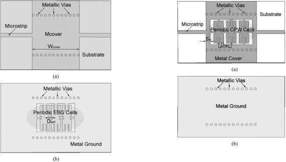
D. SIW-CPW Filter
In high-frequency system design, a large ground plane is often required for decreasing the noise generated by microwave and millimeter-wave components such as the low noise amplifier (LNA) and oscillator. In this case, the SIW-UC-EBG filter and the SIW-DGS filter are not very suitable for this type of application. In addition, the EBG and DGS structures will cause radiation losses. To enlarge the ground plane and to reduce the radiation losses, we place the UC-EBG cell on the up-cover of the SIW. As shown in Fig. 4, the space between UC-EBG cells is 


 , and it can be used to control the resonance peaks in the same way as the SIW-DGS filter can. The parameter
 is used to control the coupling between the SIW and input and output ports.
As shown in Fig. 4, the UC-EBG cells can also be considered a CPW structure, and the structure for the filter can be treated as an SIW integrated with a periodically placed CPW. Then this structure may be called the SIW-CPW filter.
Since the UC-EBG, DGS, and CPW can be fully integrated with the SIW, as shown in Figs. 2–4, as will be shown later, these structures will be ideal candidates for designing very compact wide-band filters. Since the filters are based on the construction of periodic structures, the filter synthesis is greatly simplified, and performance with a higher selectivity can be accomplished simply by inserting more cells. It can also be predicted that the SIW-CPW filter will have a small insertion loss because the SIW has a high  factor and the periodic CPW has low insertion loss characteristics [4], [19].

HAO et al.: COMPACT SUPER-WIDE BANDPASS SIW FILTERS
TABLE I
GEOMETRIC PARAMETERS OF THE SIW-EBG FILTER
Fig. 5. E-field profile for the simulated SIW-EBG filter at (a) 10 GHz and
(b) 16 GHz.
III. NUMERICAL SIMULATIONS
To demonstrate wide-band performances of those proposed filters, we have investigated those filters with the aid of a commercially available full-wave software package (Ansoft HFSS). The dielectric substrate in the simulation model has a thickness of 0.5 mm, a relative permittivity of 2.2, a loss tangent of 0.0009 at 10.0 GHz. The microstrip line width is 1.2 mm that corresponds to a 50- line on a conventional ground plane.
A. SIW-EBG Filter
An  -band SIW-EBG filter with three UC-EBG cells is studied in our design, and its geometric parameters are listed in Table I, where

 is the width of the output (or input) microstrip line,
  refers to the thickness of substrate,


 is the diameter of metallic vias, and other parameters are shown in Fig. 1.
Fig. 5 shows  -field profiles for the simulated SIW-UC-EBG filter. The
  -fields are limited in the central UC-EBG cells by metallic vias. They pass through the filter by the coupling between the UC-EBG cells at 10.0 GHz, and most of the fields are reflected by these UC-EBG cells at 16.0 GHz due to the bandgap characteristic of the UC-EBG. Fig. 5 clearly indicates that the electromagnetic fields are bounded within the central cells over the passband and are rejected by the UC-EBG cells out of the band. This suggests that the SIW can be constructed by those metallic vias with the metallic cover shown in Fig. 2, and then a high-pass behavior will take place. Due to the bandgap properties of EBG, the filter presents a bandstop performance.
2971
Fig. 6. Simulated results for the three-cell SIW-EBG filter with its geometric parameters listed in Table I.
TABLE II
GEOMETRIC PARAMETERS OF THE SIW-DGS FILTER
Fig. 6 shows simulated results of  -parameters for the studied SIW-EBG filter. The filter operates at 10.0 GHz with a relative bandwidth of nearly 35.9% (from 8.0 to 11.5 GHz). Although the conductor loss of the UC-EBG is small [1], the radiation loss is not negligible in the design. It can be found in Fig. 6 that the return loss is small over the passband (

 is better than
10 dB), but the insertion loss is increased at higher frequencies ( 2.0 dB at 11.0 GHz, for example). This is caused by the designed EBG structure which has a larger radiation loss at high frequencies than that at low frequencies.
B. SIW-DGS Filter
SIW-DGS filters with series-cascaded three and eleven UC-EBG cells are studied, respectively. Their geometric parameters are provided in Table II. The SIW is designed to have a cutoff frequency of 8.5 GHz, and the UC-EBG is designed to have a stopband at 16.5 GHz initially. By adjusting the parameters of UC-EBG cells, the SIW-DGS filter can be constructed.
Simulated results of these filters are presented in Figs. 7 and 8. It can be seen that the three-cell SIW-DGS filter has a center frequency of 11.75 GHz with a bandwidth of 55.32% over a frequency range from 8.5 to 15 GHz. The return loss is better than 11 dB. Due to its radiation characteristics and metal losses, the maximum insertion loss is 0.8 dB. Similar to the SIW-EBG
filter, the insertion loss is increased at higher frequencies. Since each individual UC-EBG cell will couple not only with
its immediate adjacent cell, but with all other cells in the periodic chain as well [4], [18], we adjust the geometric parameters

2972 |
IEEE TRANSACTIONS ON MICROWAVE THEORY AND TECHNIQUES, VOL. 53, NO. 9, SEPTEMBER 2005 |
TABLE III
GEOMETRIC PARAMETERS OF THE SIW-CPW FILTER
Fig. 7. Simulated results for the three-cell SIW-DGS filter with its geometric parameters listed in Table II.
Fig. 9. Simulated results of the three-cell SIW-CPW filter with its geometric parameters listed in Table III.
Fig. 8. Simulated results for the 11-cell SIW-DGS filter with its geometric parameters listed in Table II.
a little bit for the 11-cell SIW-DGS filter. Fig. 8 shows the simulated results for this filter. The filter has a center frequency of 12.25 GHz with a bandwidth of 61.22% (from 8.5 to 16.0 GHz). The return loss is better than 11 dB over the bandwidth. Compared to its three-cell counterpart, the 11-cell filter has a larger insertion loss that is about 1.6 dB at 8.5 GHz and increases at higher frequencies. Nevertheless, the 11-cell SIW-DGS filter has an excellent selectivity. Over a 1.0-GHz frequency range at a low sideband (from 7.5 to 8.5 GHz) and a high sideband (from 16.0 to 17.0 GHz), the transmission rejection is increased to 50 and 60 dB, respectively.
C. SIW-CPW Filter
A three-cell SIW-CPW filter and an 11-cell SIW-CPW filter have also been designed in this case. Table III lists the geometrical parameters for the three-cell SIW-CPW filter. The SIW is also designed with a cutoff frequency of 8.5 GHz, and the UC-EBG is designed to have a stopband at 15.5 GHz.
We have investigated these SIW-CPW filters using the fullwave HFSS analyzer, and simulation results are presented in Fig. 9. The three-cell SIW-CPW filter has a center frequency of 12.0 GHz with a bandwidth of 58.33% (from 8.5 to 15.5 GHz). The return loss is better than 10 dB over the bandwidth. The maximum insertion loss is 0.6 dB. It has been noticed that the insertion loss is not increased at higher frequencies. This should be attributed to the low radiation property of the CPW.
For the reasons mentioned above, we have slightly adjusted the geometric parameters for the 11-cell SIW-CPW filter. Simulated results presented in Fig. 10 show that the filter has a center frequency of 12.5 GHz with a bandwidth of 64% (from 8.5 to 16.5 GHz). The maximum insertion loss is 1.06 dB with a good selectivity. The transmission rejection is increased to 60 dB over a 1.0-GHz frequency range at both sidebands.
An interesting point can be found from Tables II and III and Figs. 7–10 that the geometric parameters for the SIW-DGS and SIW-CPW filters almost are the same in the work. This suggests that the circuits can be etched on the top cover or on the bottom cover of the SIW and the circuit performance will not be deteriorated.
IV. EXPERIMENTAL RESULTS
A microstrip line 1.2 mm wide and 60 mm long has been designed for calibration purposes, which is used to evaluate the substrate characteristics such as dielectric loss, conductor loss,

HAO et al.: COMPACT SUPER-WIDE BANDPASS SIW FILTERS
Fig. 10. Simulated results of the 11-cell SIW-CPW filter with its geometric parameters listed in Table III.
Fig. 11. Measured results for a 60-mm-long 50microstrip.
and influence of the subminiature version A (SMA) connectors in the design of these filters. Fig. 11 shows measured results that include the effect of two SMA connectors. From 4.0 to 18.0 GHz, the insertion loss is less than 0.96 dB, and the return loss is smaller than 20 dB. Such results suggest that the substrate and SMA can be used in the design.
Three-cell and 11-cell SIW-EBG filters are designed and fabricated with our standard PCB process. Fig. 12 shows photographs of those fabricated SIW-EBG filters. Measured results that include the SMA effect are shown in Figs. 13 and 14. Due to the radiation loss, these filters have a significant insertion loss. As shown in Fig. 14, the insertion losses are
3.1 dB at 11.0 GHz and 4.1 dB at 16.0 GHz, the relative bandwidth is 51.9% (from 10.0 to 17.0 GHz), and 

 is better than 10 dB in the bandwidth except for a few frequency points. Fig. 14 shows that the 11-cell SIW-EBG filter has an excellent selectivity.
Using the same substrate, we have designed three-, five-, and 11-cell SIW-DGS filters. Prototypes of these filters are fabricated and measured. Fig. 15 shows a photograph of these filters.
2973
Fig. 12. Photograph of three-cell and 11-cell SIW-EBG filters. (a) Back view.
(b) Front view.
Fig. 13. Measured results of the three-cell SIW-EBG filters.
Fig. 14. Measured results of the 11-cell SIW-EBG filters.
Figs. 16 and 17 present measured results that include two SMA effects for threeand five-cell SIW-DGS filters. These filters have a relative bandwidth of 55.32% (from 8.5 to 15.0 GHz). The three-cell SIW-DGS filter has insertion losses of 1.5 dB at

2974 |
IEEE TRANSACTIONS ON MICROWAVE THEORY AND TECHNIQUES, VOL. 53, NO. 9, SEPTEMBER 2005 |
Fig. 17. Measured results for five-cell SIW-DGS filter.
Fig. 15. Photograph of three-, five-, and 11-cell SIW-DGS filters. (a) Back view. (b) Front view.
Fig. 18. Measured and simulated results for the 11-cell SIW-DGS filter.
Fig. 16. Measured results for three-cell SIW-DGS filter.
11.0 GHz and 1.4 dB at 14.0 GHz, respectively. The five-cell SIW-DGS filter has insertion losses of 1.7 dB at 10.0 GHz and 2.0 dB at 14.0 GHz, respectively. The return losses of these two filters over the operating bandwidth are better than 10 dB. Fig. 18 shows measured results compared with simulated results for the proposed 11-cell SIW-DGS filter. This filter has an excellent selectivity performance and a small return loss lower than 10 dB in the passband. Its relative bandwidth is 61.23% (from 8.5 to 16.0 GHz). The insertion loss is 2.0 dB at 10.0 GHz and 2.6 dB at 14.0 GHz that includes the insertion
loss of two SMA connectors. Generally speaking, the measured results agree with the simulated results.
Photographs for the fabricated three-, five-, and 11-cell SIW-CPW filters are presented in Fig. 19. Measured results for the three-cell and five-cell SIW-CPW filters are presented in Figs. 20 and 21. Due to a small radiation loss of CPW, the three-cell filter has insertion losses of 0.8 dB at 10.33 GHz and 0.97 dB at 14 GHz, respectively, and the five-cell filter has insertion losses of 0.98 dB at 10.33 GHz and 1.36 dB at 14.0 GHz, respectively. The return loss for these filters are lower than 10 dB. As shown in Figs. 20 and 21, when the number of CPW cells is increased, the bandwidth is expanded slightly. The three-cell SIW-CPW filter has a relative bandwidth of 55.32% (from 8.5 to 15.0 GHz), while the five-cell SIW-CPW filter has a relative bandwidth of 58.33% (from 8.5 to 15.5 GHz).
Measured results compared with simulated results for the 11-cell SIW-CPW filter are shown in Fig. 22. This filter has a relative bandwidth of 61.23% (from 8.5 to 16.0 GHz), a return

HAO et al.: COMPACT SUPER-WIDE BANDPASS SIW FILTERS |
2975 |
Fig. 21. Measured results for the five-cell SIW-CPW filter.
Fig. 19. Photograph of the three-, five-, and 11-cell SIW-CPW filters. (a) Back view. (b) Front view.
Fig. 22. Measured and simulated results for the 11-cell SIW-CPW filter.
Fig. 20. Measured results for the three-cell SIW-CPW filter.
loss lower than 10 dB in the passband, and insertion losses of 1.3 dB at 12.0 GHz and 1.55 dB at 14.0 GHz, respectively.
With reference to the simulated results, the measured results have an excellent selectivity and a small ripple in the passband.
From the above simulated and measured results, it can be found that the SIW-EBG filter is the worst judging from the insertion loss among the proposed three types of filters. The SIW-DGS filter exhibits a moderate performance while the SIW-CPW filter demonstrated the best performance. This is mainly determined by the radiation loss. The measured and
simulated results also show that the greater the number of cells is, the bigger the insertion loss becomes. This is mainly caused by the inherent dielectric and conductor losses. In addition, the performance of selectivity is improved with increasing the number of cells in the structure. From the photographs of these filters, we can see that the proposed filters have a small size that is comparable to a coin. This makes them favorable for microwave and millimeter-wave applications.
V. CONCLUSION
Several types of compact super-wide-band SIW filters are proposed and investigated in this paper. Their prototypes are designed and fabricated on the basis of our standard PCB process. These filters allow the effective combination of the SIW scheme with periodic structures in a compact form. Simulated and measured results indicate that excellent performance of selectivity and wide passband with small insertion losses can be achieved, which may be significant for a wide range of microwave and millimeter-wave system applications.

2976 |
IEEE TRANSACTIONS ON MICROWAVE THEORY AND TECHNIQUES, VOL. 53, NO. 9, SEPTEMBER 2005 |
ACKNOWLEDGMENT
The authors are grateful to L. Yan, Y.-L. Zhang, H. Li, B. Liu, H.-J. Tang, H. Zhang, and others for their collaborations during the early stage of this work and for their many helpful comments and discussions.
REFERENCES
[1]F. R. Yang, K. P. Ma, Y. X. Qian, and T. Itoh, “A uniplanar compact photonic-bandgap (UC-PBG) structure and its applications for microwave circuits,” IEEE Trans. Microw. Theory Tech., vol. 47, no. 8, pp. 1509–1514, Aug. 1999.
[2]D. Sievenpiper, L. J. Zhang, R. F. J. Broas, N. G. Alex’opolous, and
E.Yablonovitch, “High-impedance electromagnetic surfaces with a forbidden frequency band,” IEEE Trans. Microw. Theory Tech., vol. 47, no. 11, pp. 2059–2074, Nov. 1999.
[3]M. Rahman1 and M. A. Stuchly, “Transmission line—Periodic circuit repersentation of planar microwave photonic bandgap structures,” Microw. Opt. Technol. Lett., vol. 30, pp. 15–19, Jul. 2001.
[4]J. Sor, Y. Qian, and T. Itoh, “Miniature low-loss CPW periodic structures for filter applications,” IEEE Trans. Microw. Theory Tech., vol. 49, no. 12, pp. 2336–2341, Dec. 2001.
[5]F. R. Yang, Y. X. Qian, R. Coccioli, and T. Itoh, “A novel low-loss slowwave microstrip structure,” IEEE Microw. Guided Wave Lett., vol. 8, no. 11, pp. 372–374, Nov. 1998.
[6]F. R. Yang, K. P. Ma, Y. X. Qian, and T. Itoh, “A novel TEM waveguide using uniplanar compact photonic-bandgap (UC-PBG) structure,” IEEE Trans. Microw. Theory Tech., vol. 47, no. 11, pp. 2092–2098, Nov. 1999.
[7]K. P. Ma, K. Hirose, F. R. Yang, Y. X. Qian, and T. Itoh, “Realization of magnetic conducting surface using novel photonic bandgap structure,” Electron. Lett., vol. 34, pp. 2041–2042, Oct. 1998.
[8]V. Radisic, Y. X. Qian, R. Coccioli, and T. Itoh, “Novel 2-D photonic bandgap structure for microstrip lines,” IEEE Microw. Guided Wave Lett., vol. 8, no. 2, pp. 69–71, Feb. 1998.
[9]Y. Rahmat-Samii, “The marvels of electromagnetic band gap (EBG) structures: Novel microwave and optical applications,” in Proc. SBMO/IEEE MTT-S Int. Microwave and Optoelectronics Conf., vol. 1, Sep. 2003, pp. 265–275.
[10]H. J. Hsu, M. J. Hill, R. W. Ziolkowski, and J. Papapolymerou, “A duroid-based planar EBG cavity resonator filter with improved quality factor,” IEEE Antennas Wireless Propag. Lett., vol. 1, pp. 67–70, 2002.
[11]J. Chappell, M. P. Little, and L. P. B. Katehi, “High isolation, planar filters using EBG substrates,” IEEE Microw. Wireless Comp. Lett., vol. 11, no. 6, pp. 246–248, Jun. 2001.
[12]S. T. Chew and T. Itoh, “PBG-excited split-mode resonator bandpass
filter,” IEEE Microw. Wireless Comp. Lett., vol. 11, no. 9, pp. 364–366, Sep. 2001.
[13]I. Rumsey, P. M. Melinda, and P. K. Kelly, “Photonic bandgap structures used as filters in microstrip circuits,” IEEE Microw. Guided Wave Lett., vol. 8, no. 10, pp. 336–338, Oct. 1998.
[14]F. Mernyei, I. Aoki, and H. Matsuura, “MMIC bandpass filter using par- allel-coupled CPW lines,” Electron. Lett., vol. 30, pp. 1862–1863, Oct. 1994.
[15]C. Hang, V. Radisic, Y. Qian, and T. Itoh, “High efficiency power amplifier with novel PBG ground plane for harmonic tuning,” in IEEE MTT-S Int. Microwave Symp. Dig., vol. 2, Jun. 1999, pp. 807–810.
[16]K. P. Ma, J. Kim, F. R. Yang, Y. Qian, and T. Itoh, “Leakage suppression in stripline circuits using a 2-D photonic bandgap lattice,” in IEEE MTT-S Int. Microwave Symp. Dig., vol. 1, Jun. 1999, pp. 73–76.
[17]K. Wu and R. Vahldieck, “Hybrid-mode analysis of homogeneously and inhomogeneously doped low-loss slow-wave coplanar transmission lines,” IEEE Trans. Microw. Theory Tech., vol. 39, no. 8, pp. 1348–1360, Aug. 1991.
[18]K. Wu, D. Maurin, and R. Bosisio, “An explicit design technique for wideband couplers and high quality filters using periodic topology,” in IEEE MTT-S Int. Microwave Symp. Dig., vol. 2, Jun. 1993, pp. 1085–1088.
[19]K. Wu, D. Deslandes, and Y. Cassivi, “The substrate integrated circuits—
Anew concept for high-frequency electronics and optoeletronics,” Proc. 6th Telecommunications in Modern Satellite, Cable and Broadcasting Service, vol. 1, pp. P-III–P-X, Oct. 2003.
[20]A. Piloto, K. Leahy, B. Flanick, and K. A. Zaki, “Waveguide Filters Having a Layered Dielectric Structures,” U.S. Patent 5 382 931, Jan. 17, 1995.
[21]H. Uchimura, T. Takenoshita, and M. Fujii, “Development of a ‘laminated waveguide’,” IEEE Trans. Microw. Theory Tech., vol. 46, no. 12, pp. 2438–2443, Dec. 1998.
[22]D. Stevens and J. Gipprich, “Microwave characterization and modeling of multilayered cofired ceramic waveguides,” in Proc. Int. Microelectron. Symp., San Diego, CA, Nov. 1998, pp. 195–200.
[23]F. Xu, Y. L. Zhang, W. Hong, K. Wu, and T. J. Cui, “Finite difference frequency domain algorithm for modeling guided-wave properties of substrate integrated waveguide,” IEEE Trans. Microw. Theory Tech., vol. 51, no. 11, pp. 2221–2227, Nov. 2003.
[24]J. Gipprich, D. Stevens, M. Hageman, A. Piloto, K. A. Zaki, and Y. Rong, “Embedded waveguide filters for microwave and wireless applications using cofired ceramic technologies,” in Proc. Int. Microelectron. Symp., San Diego, CA, Nov. 1998, pp. 23–26.
[25]Y. Rong, K. A. Zaki, M. Hageman, D. Stevens, and J. Gipprich;, “Low temperature cofires ceramic (LTCC) ridge waveguide bandpass chip filter,” IEEE Trans. Microw. Theory Tech., vol. 47, no. 12, pp. 2317–2324, Dec. 1999.
[26]Y. Rong, A. Zaki, J. Gipprich, M. Hageman, and D. Stevens, “LTCC wide-band ridge-waveguide bandpass filters,” IEEE Trans. Microw. Theory Tech., vol. 47, no. 9, pp. 1836–1840, Sep. 1999.
[27]Y. Rong, K. A. Zaki, M. Hageman, D. Stevens, and J. Gipprich, “Low temperature cofired ceramic (LTCC) ridge waveguide multiplexers,” in IEEE MTT-S Int. Microwave Symp. Dig., vol. 2, Jun. 2000, pp. 1169–1172.
[28]D. Deslandes and K. Wu, “Integrated microstrip and rectangular waveguide in planar form,” IEEE Microw. Wireless Comp. Lett., vol. 11, no. 2, pp. 68–70, Feb. 2001.
[29]Y. Cassivi and K. Wu, “Low cost microwave oscillator using substrate integrated waveguide cavity,” IEEE Microw. Wireless Comp. Lett., vol. 13, no. 2, pp. 48–50, Feb. 2003.
[30]D. Deslandes and K. Wu, “Millimeter-wave substrate integrated waveguide filters,” Proc. IEEE Electrical Computer Engineering Conf., vol. 3, pp. 1917–1920, May 2003.
[31]W. Q. Che, E. K. N. Yung, and K. Wu, “Millimeter-wave ferrite phase shifter in substrate integrated waveguide (SIW),” in IEEE AP-S Int. Microwave Symp. Dig., vol. 4, Jun. 2003, pp. 887–890.
[32]S. Germain, D. Deslandes, and K. Wu, “Development of substrate integrated waveguide power dividers,” in Proc. IEEE Electrical Computer Engineering Conf., vol. 3, May 2003, pp. 1921–1924.
[33]W. D’Orazio, K. Wu, and J. Helszajn, “A substrate integrated waveguide degree-2 circulator,” IEEE Microw. Wireless Comp. Lett., vol. 14, no. 3, pp. 207–209, Mar. 2004.
[34]L. Yan, W. Hong, K. Wu, and T. J. Cui, “Investigations on the propagation characteristics of SIW,” Proc. Inst. Elect. Eng. Microw., Antennas,
Propag., vol. 152, no. 1, pp. 35–42, Feb. 2005.
[35] Z. C. Hao, W. Hong, X. P. Chen, J. X. Chen, K. Wu, and T. J. Cui, “Multilayered substrate integrated waveguide elliptic filter,”
IEEE Microw. Wireless Compon. Lett., vol. 15, no. 2, pp. 1042–1045, Feb. 2005.
[36]L. Yan, W. Hong, G. Hua, J. X. Chen, K. Wu, and T. J. Cui, “Simulation and experiment on SIW slot array antennas,” IEEE Microw. Wireless Compon. Lett., vol. 14, no. 9, pp. 446–448, Sep. 2004.
[37]Y. Kimura, M. Takahashi, J. Hirokawa, M. Ando, and M. Haneishi, “76 GHz alternating-phase fed single-layer slotted waveguide arrays with suppressed sidelobes in the E-plane,” in IEEE AP-S Int. Microwave Symp. Dig., vol. 3, Jul. 2003, pp. 1042–1045.
[38]J. Hirokawa and M. Ando, “Model antenna of 76 GHz post-wall waveguide fed parallel plate slot arrays,” in IEEE AP-S Int. Microwave Symp. Dig., vol. 1, Jul. 1999, pp. 146–149.
[39], “76 GHz post-wall waveguide fed parallel plate slot array with 45 degree linear polarization,” in IEEE MTT-S Int. Microwave Symp. Dig., vol. 3, Jun. 2000, pp. 1973–1976.
[40]J. R. Bray and L. Roy, “Resonant frequencies of post-wall waveguide cavities microwaves,” in Proc. Inst. Elect. Eng. Anntennas Propag.—H, vol. 150, Oct. 2003, pp. 365–368.
[41]S. I. Yamamoto, N. Hikono, J. Hirokawa, and M. Ando, “A 120-degree beamwidth post-wall waveguide slot array with a three-way power divider on a single-layer dielectric substrate,” in Proc. IEEE Wireless Communication Technology Conf., Oct. 2003, pp. 354–355.
[42]S. H. Park, Y. Okajima, J. Hirokawa, and M. Ando, “A slotted post-wall waveguide array with inter-digital structure for 45-deg linear and dual polarization,” in IEEE AP-S Int. Microwave Symp. Dig., vol. 3, Jul. 2004, pp. 2368–2371.
[43]J. J. Simpson, A. Taflove, J. A. Mix, and H. Heck, “Computational and experimental study of a microwave electromagnetic bandgap structure with waveguiding defect for potential use as a bandpass wireless interconnect,” IEEE Microw. Wireless Comp. Lett., vol. 14, no. 7, pp. 343–345, Jul. 2004.

HAO et al.: COMPACT SUPER-WIDE BANDPASS SIW FILTERS
Zhang-Cheng Hao received the B.S. degree in electrical engineering from Xidian University, Xi’an, China, in 1997 and the M.S. degree in radio engineering from Southeast University, Nanjing, China, in 2002, where he is currently working toward the Ph.D. degree in radio engineering.
His current research interests include developing novel passive components and active devices for microwave and millimeter-wave integrated circuits. He is also interested in electromagnetic theory and computational electromagnetics.
Wei Hong (M’92) was born in Hebei Province, China, on October 24, 1962. He received the B.S. degree from the Zhenzhou Institute of Technology, Zhenzhou, China, in 1982, and the M.S. and Ph.D. degrees from Southeast University, Nanjing, China, in 1985 and 1988, respectively, all in radio engineering.
Since 1988, he has been with the State Key Laboratory of Millimeter Waves, Southeast University, where he is currently a Professor with the Department of Radio Engineering. In 1993 and each year
from 1995 to 1998, he was a short-term Visiting Scholar with the University of California at Berkeley and at Santa Cruz, respectively. He has been engaged in numerical methods for electromagnetic problems, millimeter-wave theory and technology, antennas, electromagnetic scattering, inverse scattering and propagation, RF front-end for mobile communications, and the parameters extraction of interconnects in VLSI circuits. He has authored and coauthored over 200 technical publications and authored the book Principle and Application of the Method of Lines (Nanjing, China: Southeast Univ. Press, 1993, in Chinese). He has served as a reviewer for Proceedings of the Institution of Electrical Engi- neering—H, and Electron Letters.
Dr. Hong is a senior member of the Chinese Institute of Engineering and has served as the reviewer for many technique journals, including the IEEE TRANSACTIONS ON MICROWAVE THEORY AND TECHNIQUES. He was the recipient of the First-Class Science and Technology Progress Prizes issued by the State Education Commission in 1992 and 1994, respectively, the Fourth-Class National Natural Science Prize in 1991, and the Third-Class Science and Technology Progress Prize of Jiangsu Province. In addition, he was the receipient of the Foundation for China Distinguished Young Investigators of the National Science Foundation of China.
Ji-Xin Chen was born in Jiangsu Province, China, in 1976. He received the B.S. and M.S. degrees in radio engineering from Southeast University, Nanjing, China, in 1998 and 2002, respectively, where he is currently working toward the Ph.D. degree.
His current research interests include microwave and millimeter-wave circuit and monolithic microwave IC design.
2977
Xiao-Ping Chen received the B.S. and M.S.E. degrees from Harbin Institute of Technology, Harbin, China, in 1997 and 1999, respectively, and the Ph.D. degree in electrical engineering from Huazhong University of Science and Technology, Wuhan, China, in 2003. His dissertation focused on dielectric resonator filter and microwave measurement.
He is currently a Postdoctoral Associat with the State Key Laboratory of Millimeter Waves, Southeast University, Nanjing, China, where he is involved with microwave and millimeter-wave circuits for commu-
nication systems applications.
Ke Wu (M’87–SM’92–F’01) is a Professor of electrical engineering and Tier-I Canada Research Chair in Radio-Frequency and Millimeter-Wave Engineering. He was a Visiting or Guest Professor with many universities around the world. He also holds an honorary Visiting Professorship and a Cheung Kong endowed Chair Professorship (visiting) at the Southeast University, Nanjing, China, and an honorary Professorship with the Nanjing University of Science and Technology, Nanjing, China. He has been the Director of the Poly-Grames Research
Center, Department of Electrical Engineering, Ecole Polytechnique, University of Montreal, Montreal, QC, Canada, as well as the Founding Director of the Canadian Facility for Advanced Millimeter-Wave Engineering (FAME). He has authored or coauthored over 390 referred papers and several books and book chapters. His current research interests involve hybrid/monolithic planar and nonplanar integration techniques, active and passive circuits, antenna arrays, advanced field-theory-based CAD and modeling techniques, and development of low-cost RF and millimeter-wave transceivers. He is also interested in the modeling and design of microwave photonic circuits and systems. He serves on the Editorial Board of Microwave Journal, Microwave and Optical Technology Letters and Wiley’s Encyclopedia of RF and Microwave Engineering. He is an Associate Editor for the International Journal of RF and Microwave Computer-Aided Engineering (RFMiCAE).
Dr. Wu is a Fellow of the Canadian Academy of Engineering (CAE) and a member of the Electromagnetics Academy, Sigma Xi, and the URSI. He has held many positions in and has served on various international committees, including as the Vice Chairperson of the Technical Program Committee (TPC) for the 1997 Asia-Pacific Microwave Conference, the General Co-Chair of the 1999 and 2000 SPIE’s International Symposium on Terahertz and Gigahertz Electronics and Photonics, the General Chair of the Eighth International Microwave and Optical Technology (ISMOT’2001), the TPC Chair of the 2003 IEEE Radio and Wireless Conference (RAWCON’2003), and the General Co-Chair of the RAWCON’2004. He has served on the Editorial or Review Boards of various technical journals, including the IEEE TRANSACTIONS ON MICROWAVE THEORY AND TECHNIQUES, the IEEE TRANSACTIONS ON ANTENNAS AND PROPAGATION, and the IEEE MICROWAVE AND WIRELESS COMPONENTS LETTERS. He served on the 1996 IEEE Admission and Advancement Committee and the Steering Committee for the 1997 joint IEEE Antennas and Propagation Society (AP-S)/URSI International Symposium. He has also served as a TPC member for the IEEE Microwave Theory and Techniques Society (IEEE MTT-S) International Microwave Symposium. He was elected into the Board of Directors of the Canadian Institute for Telecommunication Research (CITR). He is currently the chair of the joint IEEE chapters of MTTS/APS/LEOS in Montreal, QC, Canada, and the Chapter Coordinator for MTT-S Region 7. He was the recipient of a URSI Young Scientist Award, Oliver Lodge Premium Award of the Institute of Electrical Engineer (IEE), U.K., the Asia-Pacific Microwave Prize, the University Research Award “Prix Poly 1873 pour l’Excellence en Recherche” presented by the Ecole Polytechnique on the occasion of its 125th anniversary, the UrgelArchambault Prize (the highest honor) in the field of physical sciences, mathematics and engineering from the French-Canadian Association for the Advancement of Science (ACFAS), and the 2004 Fessenden Medal of the IEEE Canada. In 2002, he was the first recipient of the IEEE MTT-S Outstanding Young Engineer Award.