

диафрагмированные волноводные фильтры / 9dc3a59d-c74e-4cfc-ac1f-f8c87612756a
.pdf142 |
IEEE TRANSACTIONS ON MICROWAVE THEORY AND TECHNIQUES, VOL. 56, NO. 1, JANUARY 2008 |
Substrate Integrated Waveguide Cross-Coupled
Filter With Negative Coupling Structure
Xiao-Ping Chen and Ke Wu, Fellow, IEEE
Abstract—Substrate integrated waveguide (SIW) technology provides an attractive solution to the integration of planar and nonplanar circuits by using a planar circuit fabrication process. However, it is usually difficult to implement the negative coupling structure required for the design of compact canonical folded elliptic or quasi-elliptic cross-coupled bandpass filter on the basis of a single-layer SIW. In this paper, a special planar negative coupling scheme including a magnetic coupling post-wall iris and a balanced microstrip line with a pair of metallic via-holes is studied in detail. Two  -band fourth-degree cross-coupled bandpass filters without and with source–load coupling using the negative coupling structures are then proposed and designed. The two novel SIW filters having the same center frequency of 20.5 GHz and respective passband width of 700 and 800 MHz are implemented on a single-layer Rogers RT/Duroid 5880 substrate with thickness of 0.508 mm. Measured results of those filters, which exhibit a high selectivity, and a minimum in-band insertion loss of approximately 0.9 and 1.0 dB, respectively, agree well with simulated results.
Index Terms—Cross-coupled structure, filter, negative coupling, quasi-elliptic, substrate integrated waveguide (SIW).
I. INTRODUCTION
ELLIPTIC OR quasi-elliptic filters with finite transmission zeros are now finding ever-increasing applications in a wide range of wireless and mobile communication and sensing systems due to their high performance and compact size. In general, cross-coupling between nonadjacent resonators in the elliptic or quasi-elliptic filters is required to bring up the transmission zeros from infinity to finite positions in the complex plane. These filters provide multiple paths through which a signal may pass between the input and output ports so that a signal cancellation can take place at given finite frequencies for enhancing a skirt selectivity, or at given imaginary frequencies for achieving a flat group delay, or even both simultaneously, depending on the phase and magnitude conditions of signals
[1], [2].
It has been understood that both positive and negative coupling are needed to generate transmission zeros at finite frequencies for achieving a high selectivity in a cross-coupled filter [3]. Positive coupling can conveniently be obtained by a magnetic coupling structure, e.g., an inductive iris directly realized by a waveguide cavity narrow wall. However, it is not easy in
Manuscript received June 11, 2007; revised August 17, 2007. This work was supported by the National Science and Engineering Research Council (NSERC) of Canada.
The authors are with the Département de Génie Électrique, Poly-Grames Research Center, École Polytechnique de Montreal, Montreal, QC, Canada H3C 3A7 (e-mail: xiao-ping.chen@polymtl.ca; ke.wu@polymtl.ca).
Color versions of one or more of the figures in this paper are available online at http://ieeexplore.ieee.org.
Digital Object Identifier 10.1109/TMTT.2007.912222
many cases to produce a negative coupling to which special attention should be paid. To obtain the negative coupling in a waveguide combline resonator filter, the length of metal rod has to be greater than 45 and the coupling slot should be placed at the open side of the rod [4]. Electrical probe that needs a repeated fine machining is also used to achieve a nonadjacent electrical coupling in the combline filter [5], [6]. A square aperture at the center of the broad walls of the coupling top and bottom cavities can be used to generate the required negative coupling in a canonical folded waveguide filter [7], [8]. In the dielectric-loaded waveguide filter, a probe connecting the top of the first cavity to the base of the second provides the sign inversion of inline coupling for the negative coupling [9]. A configuration using staggered


 dielectric resonator modes was presented to obtain the negative coupling for dielectric resonator elliptic filter [10]. The negative J-inverter can be replaced with three positive J-inverters on the basis of the equivalence in dielectric resonator band rejection filter [10].


 resonance is excited only in resonator 3 of the fourth-order
  -plane waveguide filter, which exhibits a magnetic iris coupling, and the coupling between resonators 1 and 4 becomes negative by placing the coupling slot between resonators 2 and 3 in the second half of resonator 3 because


 mode cavities are introduced for the transformation of 0
 and 180
 phases of cross-cou- pling [11], [12].
For the emerging substrate integrated waveguide (SIW) technology, which has already been proven to be effective in the integration of planar and nonplanar circuits by using a planar circuit fabrication process [13], [14], only magnetic iris coupling can be implemented on a single-layer substrate. The last two techniques of the above-mentioned schemes have successfully been used for the design of SIW elliptic or quasi-elliptic filters [15], [16]. In this paper, a negative coupling structure presented in [17] is the first of all investigated in detail and is then used to realize a cross-coupled filter with a quasi-elliptic response and more compact size made of a single-layer SIW. This paper is organized as follows. In Section II, the negative coupling structure including a magnetic coupling iris and a balanced microstrip line with a pair of metallized via-holes is investigated, and then a fourth-degree SIW cross-coupled filter without source–load coupling using the negative coupling structure is synthesized, designed, and measured. Section III provides the synthesis, realization, and experiments of a fourth-degree SIW cross-cou- pled filter with source–load coupling using the negative coupling structure. Finally, Section IV concludes this study.
II.FOURTH-DEGREE CROSS-COUPLED FILTER
WITHOUT SOURCE–LOAD COUPLING
Fig. 1 shows the geometric configuration and schematic topology of the proposed SIW quasi-elliptic filter without
0018-9480/$25.00 © 2007 IEEE

CHEN AND WU: SIW CROSS-COUPLED FILTER WITH NEGATIVE COUPLING STRUCTURE |
143 |
Fig. 1. (a) Geometric configuration of the proposed SIW cross-coupled filter without source–load coupling using the negative coupling structure.
(b) Schematic topology of the proposed SIW cross-coupled filter without source–load coupling using the negative coupling structure. (Source: S, load: L, resonator: R.)
source–load coupling on the basis of the negative coupling structure. Except for the coupling between 


 -mode-based SIW cavity resonators 2 and 3, all the other coupling between two


 -mode-based SIW cavity resonators are obtained by magnetic post-wall irises, which provide positive coupling.


 -mode-based SIW cavity resonators 1 and 4 are directly excited by and connected to 50-
 microstrip lines with coupling slots. A structure including a magnetic coupling post-wall iris and a balanced microstrip line with a pair of metallized via-holes is placed between


 -mode-based SIW cavity resonators 2 and 3 to invert the phase of the signal. Therefore, mixed coupling, including both positive and negative coupling, which cancel each other, is produced. The structure can be optimized to ensure that the negative coupling is stronger than its positive coupling counterpart and a small amount of the negative coupling can be canceled out by tuning the width of the magnetic post-wall iris. This structure is well suited for SIW implementation and provides an accurate negative coupling with an inductive post-wall iris.
A. Circuit Synthesis
To design the cross-coupled filters, the first step is to synthesize a low-pass prototype, which meets a given specification and also determines an appropriate coupling matrix. The synthesis of the filter generally follows three steps. First, poles and
zeros of the transfer function should be obtained according to the specification of the filter. Then generalized element values or generalized coupling matrix of the low-pass prototype circuit can be obtained. At last, we can calculate the design parameters by denormalizing the generalized element values. The generalized coupling matrix for the quasi-elliptic filter with transmission zeros at 


 and in-band return loss of 25 dB can be obtained by optimization [18] (see (1) at the bottom of this page). The generalized coupling matrix is denormalized by using the following formula:
(2)
where 

 is the relative bandwidth,
 is the absolute bandwidth, and
  is the center frequency. Thus, we can obtain the design parameters for the filter with the center frequency of


 GHz and the absolute bandwidth of


 MHz as follows:


 ,
, 


 ,
, 


 ,
,


 .
.
B. Cavity Size
The initial size of the 


 -mode-based SIW cavity can be determined by setting the resonant frequency to the center frequency of filter by using the following formula [19]:
(3)
where
(4)
 and
and  are the width and length of the


 -mode-based SIW cavity, respectively.
  and
and  are the diameter of metallized viaholes and center-to-center pitch between two adjacent via-holes.
 is the light velocity in vacuum, and
 is the dielectric constant of the substrate.
C. Internal Coupling
To determine the internal coupling coefficients, a pair of coupled 


 -mode-based SIW cavity resonators with input and output is simulated by using a commercial full-wave electromagnetic simulator [Ansoft’s High Frequency Structure Simulator (HFSS)]. Figs. 2 and 3 display simulated frequency responses on the basis of the negative coupling and positive coupling, respectively. From each type of coupling curve, two split resonant-mode frequencies can easily be identified by two resonant peaks. As a result, it can be concluded that the larger
(1)

144 |
IEEE TRANSACTIONS ON MICROWAVE THEORY AND TECHNIQUES, VOL. 56, NO. 1, JANUARY 2008 |
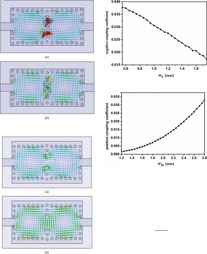
Fig. 2. Coupling structure and typical frequency responses for electric coupling with different width of post-wall iris (d = 0:5 mm, p = 1 mm, r = 0:55 mm,
wslot = 0:25 mm).
the width of post-wall iris is in the negative coupling structure, the narrower the separation of the two modes becomes. This suggests that the negative coupling becomes weaker because a greater amount of the negative coupling is cancelled by the positive coupling. It can also be observed that the larger the width of the post-wall iris is in the positive coupling structure, the wider the separation of the two modes becomes. This indicates that the positive coupling becomes stronger. It can be noted that the high-mode frequency of the positive coupling and the low-mode frequency of the electric coupling remain unchanged regardless of the iris size or coupling strength. Figs. 4 and 5 plot the magnetic field distributions of the low and high modes for both positive and negative coupling. As we can see, the magnetic field of
Fig. 3. Coupling structure and typical frequency responses for magnetic coupling with different width of post-wall iris (d = 0:5 mm, p = 1 mm).
the high mode near the coupling section is parallel to the symmetry plane, while the magnetic field of the low mode near the coupling section is perpendicular to the symmetry plane for the positive coupling structure. On the contrary, the magnetic field of the high mode near the coupling section is perpendicular to the symmetry plane, while the magnetic field of the low mode near the coupling section is parallel to the symmetry plane for the negative coupling structure.
The coupling coefficient can then be extracted by using the following relation [20]:
(5)
where  and
and  stand for the high and low resonant frequencies, respectively, and
  represents the coupling coefficient between
CHEN AND WU: SIW CROSS-COUPLED FILTER WITH NEGATIVE COUPLING STRUCTURE |
145 |
Fig. 6. Negative coupling coefficient of the coupling structure.
Fig. 4. Magnetic field distribution for negative coupling. (a) Low mode.
(b) High mode.
Fig. 7. Positive coupling coefficient of the coupling structure.
Fig. 5. Magnetic field distribution for positive coupling. (a) Low mode.
(b) High mode.
two SIW cavity resonators. With the results presented in Figs. 2 and 3 and (4), design curves depicted in Figs. 6 and 7 are obtained for electric and magnetic coupling coefficients.
D. External Coupling
Numerical analysis is carried out on a 


 -mode-based SIW cavity resonator with 50-
 microstip lines as its input/output to determine the external quality factor using Ansoft’s HFSS package. The coupling is controlled by changing the length of coupling slot with a fixed coupling slot width of 0.25 mm and a fixed post-wall iris width of 3.1 mm. The external quality factor
 is calculated by [20]
(6)
 dB
dB
where  is the frequency at which
 reaches its maximum value and
 dB is the 3-dB bandwidth for which
 is reduced by 3 dB from its maximum value. Fig. 8 shows the calculated
 dependent on the length of coupling slot.
E. Filter Tuning
The design parameters are used to estimate the initial sizes of the entire filter shown in Fig. 1 through the use of design curves, as shown in Fig. 6–8. A fine-tuning procedure is used to optimize the entire filter. Table I gives dimensions of the filter

146 |
IEEE TRANSACTIONS ON MICROWAVE THEORY AND TECHNIQUES, VOL. 56, NO. 1, JANUARY 2008 |
TABLE I
DIMENSIONS OF THE PROPOSED SIW CROSS-COUPLING FILTER
WITHOUT SOURCE–LOADING COUPLING
Fig. 8. Typical external quality factor of the input/output structure (d = 0:5 mm, p = 1 mm, w
 = 3:1 mm).
whose simulated response is depicted in Fig. 9 altogether with the ideal circuit response with 
 of 500.
F. Experiments
The filter was designed and implemented on the substrate of Rogers RT/Duroid 5880 with its height of 0.508 mm by using linear arrays of metallized via-hole having the diameter of 0.5 mm and the center-to-center pitch of 1 mm, which can be made with our laboratory printed circuit board (PCB) process. A photograph of the developed filter is displayed in Fig. 10. In our experiments, the Anritsu 37397C vector network analyzer and Anritsu Wiltron 3680-K test fixture are used to measure the filter. A thru-reflect-line (TRL) calibration is performed in order to remove effects of the test fixture. Fig. 11 depicts simulated and measured frequency responses. The measured in-band return loss is below 19 dB, while the measured minimum in-band insertion loss is approximately 0.9 dB. The insertion loss would mainly be attributed to the dielectric loss and conductor loss. The measured results are in good agreement with the simulated ones.
III. FOURTH-DEGREE CROSS-COUPLED FILTER
WITH SOURCE–LOAD COUPLING
The source–load coupling can be used to further improve the slope selectivity of canonical folded cross-coupled filters. The
Fig. 9. Ideal circuit response and simulated response of the proposed SIW quasi-elliptic filter.
main advantage of these filters with source–load coupling is that they allow a better control of the stopbands since they can implement up to  finite transmission zeros (in a filter of order
  ) instead of only

 when the source and load are coupled to only one resonator each. Obviously, the additional two transmission zeros can be used to either improve the stopband or the in-band group delay, and they would not yield any significant effect on the passband, which is controlled by the number of resonators. However, the positions of transmission zeros are

CHEN AND WU: SIW CROSS-COUPLED FILTER WITH NEGATIVE COUPLING STRUCTURE |
147 |
Fig. 10. Proposed SIW quasi-elliptic filter.
Fig. 11. Measured and simulated responses of proposed SIW quasi-elliptic filter.
very sensitive to a small change in dimensions of the coupling structure between source and load [21].
The geometric configuration of the proposed fourth-degree quasi-elliptic SIW filter with source–load coupling and its corresponding topology are described in Fig. 12. All the direct coupling are realized by magnetic post-wall irises, which provide positive coupling. The cross-coupling between 


 -mode- based SIW cavity resonators 1 and 4 is a negative coupling, which is implemented by the structure including a magnetic coupling iris and a balanced microstrip line with a pair of metallized via-holes for mixed coupling. Similarly, the structure is optimized to ensure that the negative coupling is larger than the
Fig. 12. (a) Geometric configuration of the proposed SIW cross-coupled filter with source–load coupling by using the negative coupling structure.
(b) Schematic topology of proposed SIW cross-coupled filter with source–load coupling by using the negative coupling structure. (Source: S, load: L, resonator: R.)
positive coupling and a small amount of such a negative coupling can be canceled by tuning the width of magnetic post-wall iris. The first/fourth SIW cavity resonator is excited by a section of SIW, which is very convenient to realize the source–load coupling by magnetic coupling post-wall iris for the positive coupling. A linear microstrip taper is used to realize the transition between the 50- microstip line and SIW [14].
A. Circuit Synthesis
The low-pass prototype can be synthesized by the same procedure as presented in Section II. The generalized coupling matrix for a fourth-degree quasi-elliptic filter with transmission zeros at 


 and
and 


 and in-band return loss of 20 dB is given in (7), shown at the bottom of this page. Formula (2) is used to denormalize the above generalized coupling matrix for the design parameters of the filter with the center frequency
of |
GHz and the absolute bandwidth of |
|
|
MHz. They are given as follows: |
|
, |
|
, |
, |
, and |
. |
(7)

148 |
IEEE TRANSACTIONS ON MICROWAVE THEORY AND TECHNIQUES, VOL. 56, NO. 1, JANUARY 2008 |
TABLE II
DIMENSIONS OF THE PROPOSED SIW CROSS-COUPLED FILTER
WITH SOURCE–LOAD COUPLING
Fig. 14. Proposed SIW cross-coupled filter with source–load coupling.
Fig. 13. Measured and simulated responses of the proposed SIW cross-coupled filter with source–load coupling.
B. Realization by SIW
The procedure similar to that in Section II is used to design the filter. According to (5), a pair of 


 -mode-based SIW cavity resonators coupled by a post-wall iris with input/output is numerically analyzed by the Ansoft’s HFSS package to evaluate the internal positive coupling, while a pair of


 -mode- based SIW cavity resonators are coupled by the negative coupling structure for the internal negative coupling. Based on (6), the


 -mode-based SIW cavity resonator doubly loaded by two sections of SIW for the input and output using a post-wall iris is also numerically analyzed by the Ansoft’s HFSS package to extract the external quality factor. A section of SIW with a post-wall iris is used to extract the source–load coupling.
In the end, the entire filter is fine tuned to meet the specifications given above. The dimensions of the filter are given in Table II. The full-wave simulation results are also depicted in Fig. 13.
C. Experiments
package. The measured in-band return loss is below 15 dB, while the measured minimum in-band insertion loss is approximately 1.0 dB. The dielectric loss of substrate and conductor loss are responsible for the insertion loss. The measured results are in good agreement with the simulated ones, except that there is a slight frequency shift of approximately 0.5%.
IV. CONCLUSIONS
A planar structure compatible with emerging SIW technology was studied in detail and used to obtain negative coupling for the design of a canonical folded cross-coupling bandpass filter with a quasi-elliptic response. This structure provides the mixed coupling for which the negative coupling can be greater than the positive coupling for optimized dimensions, and also the coupling can be accurately modified by tuning the dimensions of the positive coupling section.
Subsequently, two fourth-degree SIW cross-coupled filters without and with source–load coupling were proposed and implemented over the  -band on the basis of a single-layer Rogers RT/Duroid 5880 substrate with a thickness of 0.508 mm. It has been found theoretically and experimentally that the proposed filters have very good selectivity, low insertion loss, and com- pact-size geometry, and they can be directly integrated and made with other planar circuits at a low cost for a wide range of microwave and millimeter-wave applications.
ACKNOWLEDGMENT
The authors express their gratitude to J. Gauthier, R. Brassard, and S. Dube, all with the Département de Génie Électrique, Poly-Grames Research Center, École Polytechnique de Montreal, Montreal, QC, Canada, for their technical assistance in fabricating the experimental prototypes.
Rogers RT/Duroid 5880 with a height of 0.508 mm is used to realize the filter by our low-cost standard PCB process. The diameter and center-to-center pitch of the metallized via-holes are also 0.5 and 1 mm, respectively. A photograph of the filter is given in Fig. 14. The filter is measured by using an Anritsu 37397C vector network analyzer and an Anritsu Wiltron 3680-K test fixture. The effect of the test fixture is removed by applying a TRL calibration. Measured results are depicted in Fig. 13, compared with simulated results obtained by using Ansoft’s HFSS
REFERENCES
[1]A. E. Atia and A. E. Williams, “Narrow bandpass waveguide filters,”
IEEE Trans. Microw. Theory Tech., vol. MTT-20, no. 4, pp. 258–265, Apr. 1972.
[2]R. Levy, “Filters with single transmission zeros at real and imaginary frequencies,” IEEE Trans. Microw. Theory Tech., vol. MTT-24, no. 4, pp. 172–181, Apr. 1976.
[3]J.-S. Hong and M. J. Lancaster, “Couplings of microstrip square open-loop resonators for cross-coupled planar microwave filters,”
IEEE Trans. Microw. Theory Tech., vol. MTT-24, no. 12, pp. 2099–2109, Dec. 1976.

CHEN AND WU: SIW CROSS-COUPLED FILTER WITH NEGATIVE COUPLING STRUCTURE |
149 |
[4]H. W. Yao, K. A. Zaki, A. E. Atia, and R. Hershtig, “Full wave modeling of conducting posts in rectangular waveguides and its applications to slot coupled combline filters,” IEEE Trans. Microw. Theory Tech., vol. 43, no. 12, pp. 2824–2829, Dec. 1995.
[5]C. Wang and K. A. Zaki, “Full wave modeling of electric coupling probes comb-line resonators and filters,” IEEE Trans. Microw. Theory Tech., vol. 48, no. 12, pp. 2459–2464, Dec. 1995.
[6]C. Wang, K. A. Zaki, A. E. Atia, and T. G. Dolan, “Dielectric combline resonators and filters,” IEEE Trans. Microw. Theory Tech., vol. 46, no. 12, pp. 2501–2506, Dec. 1998.
[7]T. Shen, H.-T. Hsu, K. A. Zaki, A. E. Atia, and T. G. Dolan, “Full-wave design of canonical waveguide filters by optimization,” IEEE Trans. Microw. Theory Tech., vol. 51, no. 2, pp. 504–510, Feb. 2003.
[8]J. A. Ruiz-Cruz, M. A. E. Sabbagh, K. A. Zaki, J. M. Rebollar, and
Y.Zhang, “Canonical ridge waveguide filters in LTCC or metallic resonators,” IEEE Trans. Microw. Theory Tech., vol. 53, no. 1, pp. 174–182, Jan. 2005.
[9]V. Walker and I. C. Hunter, “Design of cross-coupled dielectric-loaded waveguide filters,” Proc. Inst. Elect. Eng.—Microw. Antennas Propag., vol. 148, pp. 91–96, Apr. 2001.
[10]S. Verdeyme and P. Guilion, “Direct coupling configuration between TE
 dielectric resonator modes application to the design of an elliptic microwave filter,” in IEEE MTT-S Int. Microw. Symp. Dig., Jun. 1990, pp. 223–226.
[11]U. Rosenberg, “New planar waveguide cavity elliptic function filters,” in Eur. Microw. Symp. Dig., 1995, pp. 524–527.
[12]J. A. Ruiz-Cruz, M. A. E. Sabbagh, K. A. Zaki, J. M. Rebollar, and
Y.Zhang, “Canonical ridge waveguide filters in LTCC or metallic resonators,” IEEE Trans. Microw. Theory Tech., vol. 53, no. 1, pp. 174–182, Jan. 2005.
[13]K. Wu, “Integration and interconnect techniques of planar and nonplanar structures for microwave and millimeter-wave circuits-current status and future trend,” in Proc. Asia–Pacific Microw. Conf., Taiwan, R.O.C., Dec. 2001, pp. 411–416.
[14]D. Deslandes and K. Wu, “Integrated microstrip and rectangular waveguide in planar form,” IEEE Microw. Wireless Compon. Lett., vol. 11, no. 2, pp. 68–70, Feb. 2001.
[15]X.-P. Chen, W. Hong, T. Cui, Z. Hao, and K. Wu, “Substrate integrated waveguide elliptic filter with transmission line inserted inverter,” Electron. Lett., vol. 41, pp. 851–852, 2005.
[16]X.-P. Chen, W. Hong, J. Chen, and K. Wu, “Substrate integrated waveguide elliptic filter with high mode,” in Proc. Asia–Pacific Microw. Conf., Suzou, China, Dec. 2005, pp. 3–3.
[17]C.-Y. Chang and W.-C. Hsu, “Novel planar, square-shaped, dielec- tric-waveguide, single-, and dual-mode filters,” IEEE Trans. Microw. Theory Tech., vol. 50, no. 11, pp. 2527–2536, Nov. 2002.
[18]S. Amari, “Synthesis of cross-coupled resonator filters using an analytical gradient-based optimization technique,” IEEE Trans. Microw. Theory Tech., vol. 48, no. 9, pp. 1559–1564, Sep. 2000.
[19]Y. Cassivi, L. Perregrini, P. Arcioni, M. Bressan, K. Wu, and G. Conciauro, “Dispersion characteristics of substrate integrated rectangular waveguide,” IEEE Microw. Wireless Compon. Lett., vol. 12, no. 2, pp. 333–335, Feb. 2002.
[20]J.-S. Hong and M. J. Lancaster, Microstrip Filter for RF/Microwave Applications. New York: Wiley, 2001.
[21]E. Ofli, R. Vahldieck, and S. Amari, “Novel E-plane filters and diplexers with elliptic response for millimeter wave applications,”
IEEE Trans. Microw. Theory Tech., vol. 53, no. 3, pp. 843–851, Mar. 2005.
Xiao-Ping Chen was born in Hubei Province, China, in 1974. He received the Ph.D. degree in electrical engineering from Huazhong University of Science and Technology, Wuhan, China, in 2003.
From 2003 to 2006, he was a Post-Doctoral Researcher with the State Key Laboratory of Mil- limeter-Waves, Radio Engineering Department, Southeast University, Nanjing, China, where he was involved with the advanced microwave and millimeter-wave circuit for communication system applications under the financial support of the
China Post-Doctoral Fund. He is currently a Post-Doctoral Fellow with the Département de Génie Électrique, Poly-Grames Research Center, École Polytechnique de Montreal, Montreal, QC, Canada. He has authored or coauthored over 20 papers in referred journals and conference proceedings. His research interests are dielectric resonator filters and antennas, microwave measurement, and substrate integrated circuits (SICs) for microwave and millimeter-waves applications.
Ke Wu (M’87–SM’92–F’01) is Professor of electrical engineering, and Tier-I Canada Research Chair in RF and millimeter-wave engineering with the École Polytechnique de Montréal, Montréal, QC, Canada. He also holds a Cheung Kong endowed chair professorship (visiting) with Southeast University, and an honorary professorship with the Nanjing University of Science and Technology, Nanjing, China, and the City University of Hong Kong. He has been the Director of the Poly-Grames Research Center. He has authored or coauthored
over 515 referred papers and several books/book chapters. He has served on the Editorial/Review Boards of numerous technical journals, transactions, and letters, including being an Editor and Guest Editor. His current research interests involve substrate integrated circuits (SICs), antenna arrays, advanced computer-aided design (CAD) and modeling techniques, and development of low-cost RF and millimeter-wave transceivers and sensors. He is also interested in the modeling and design of microwave photonic circuits and systems.
Dr. Wu is a Fellow of the Canadian Academy of Engineering (CAE) and the Royal Society of Canada (The Canadian Academy of the Sciences and Humanities). He is a member of the Electromagnetics Academy, Sigma Xi, and URSI. He has held key positions in and has served on various panels and international committees including the chair of Technical Program Committees, International Steering Committees, and international conferences/symposia. He is currently the chair of the joint IEEE Chapters of the Microwave Theory and Techniques Society (MTT-S)/Antennas and Propagation Society (AP-S)/Lasers and Electro-Optics Society (LEOS), Montréal, QC, Canada. He is an elected IEEE MTT-S Administrative Committee (AdCom) member for 2006–2009 and serves as the chair of the IEEE MTT-S Transnational Committee. He was the recipient of many awards and prizes including the first IEEE MTT-S Outstanding Young Engineer Award.