

диафрагмированные волноводные фильтры / 3ede4f42-578c-454b-9a71-63b7546abf58
.pdfIET Microwaves, Antennas & Propagation
Research Article
Realisation of carved and iris groove gap waveguide filter and E-plane diplexer for V- band radio link application
Morteza Rezaee1  , Ashraf Uz Zaman2
1Department of Electrical Engineering, Hakim Sabzevari University, Sabzevar, Iran 2Department of Signals and Systems, Chalmers University of Technology, Gothenburg, Sweden
 E-mail: morteza.rezaee@hsu.ac.ir
ISSN 1751-8725
Received on 29th March 2017 Revised 27th July 2017 Accepted on 30th July 2017 E-First on 4th October 2017 doi: 10.1049/iet-map.2017.0268 www.ietdl.org
Abstract: The gap waveguide technology is a promising candidate as a cost-effective and low-loss platform for realizing microwave devices particularly at frequencies higher than 40 GHz. In this study, two types of groove gap waveguide filters and also a diplexer are presented. Coupling mechanism of these filters is based on carving on the pin plate and iris between adjacent cavities. Two fifth-order Chebyshev filters are realised at 62.5 GHz. The proposed diplexer consists of RX and TX iris groove gap waveguide filters at the centre frequency of 59.5 and 62.5 GHz and an E-plane groove gap waveguide T-junction. The required transition of the groove gap waveguide to WR-15 is designed and used as an input port of the filters. Moreover, E- plane groove gap waveguide T-junction is designed as the connecting part of the groove gap waveguide filters to the WR-15 antenna port. Finally all parts are integrated. The proposed diplexer is manufactured in aluminium by sawing and milling and then silver plating is done. The RX and TX passbands of the diplexer is around 1.7 and 2.4% with the measured return loss better than 13.6 dB and minimum insertion loss of 0.9 and 0.8 dB, respectively.
1 Introduction
Emerging commercial millimeter-wave (mm-wave) technology applications, such as high-speed wireless local area network and point-to-point radio link, require a design platform of high performance, low-cost fabrication and high reliability. Also, integrating different parts of the mm-wave circuit to a compact package should be possible by using this platform to eliminate the need for transitions between different technologies. Highperformance conventional hollow waveguide technology is a suitable choice to satisfy some mm-wave circuit requirements, such as low-insertion loss, good shielding and high-power handling capability. Traditionally, the hollow waveguide components are fabricated by the so-called split block technique, i.e. by combining two separate metal parts by using screws. Good electrical contact between these two parts is vital to achieve low-insertion loss and high-quality factor, and also to avoid passive intermodulation [1] in high-power applications. This issue increases the complexity and fabrication cost at mm-waves because the joining surfaces must be very smooth in the connection region. Another problem dealing with hollow waveguides is the integration of active circuits. On the other hand, planar platforms such as microstrip or substrate integrated waveguide (SIW), provide the mounting of active circuit components on the substrate, but lead to high-insertion loss due to the substrate and leakage [2, 3].
The gap waveguide technology is a promising low-cost and high-performance platform for making low insertion loss circuits at frequencies above 40 GHz [4]. The main concept of gap waveguide technology is based on preventing wave propagation at a specific frequency band and at the same time, providing a transmission line to guide the waves across this forbidden propagation area [5]. The stopband characteristic is in principle realised by using a structure consisting of a perfect electric conductance (PEC) surface paralleled with a perfect magnetic conductance (PMC) surface with distance of <λ/4. The PMC surface can, e.g. be realised by periodic metallic pins, so-called bed of nails [6], or by mushroom-type periodic structure [7]. Based on the transmission line structure used for wave propagation, three types of gap waveguides have been proposed which are called groove, ridge, and microstrip gap waveguides [3, 8, 9]. Analytic studies of propagation characteristics in gap waveguides are presented in [10], and
numerical stopband studies in [7]. The wave propagation in the ridge and microstrip gap waveguides is quasi-transverse electromagnetic and in the groove gap waveguide, which has a higher quality factor than other ones [11], it is TE like [12]. So far, several microwave and mm-wave components by using gap waveguide technology have been realised such as, antennas [13– 16], filters [17–21], coupler [22], and transitions [23, 24]. Also, by using the electromagnetic stopband phenomenon of the gap waveguide, it has found applications in packaging of microwave monolithic integrated circuits [25] and microstrip filters [26], such as removing undesired resonances and improving isolation between components and high power handling capability.
Diplexers are used at the front end of transceivers to separate the RX and TX signals and at the same time, connect the receiver and transmitter circuits to the antenna port. A diplexer should have a low-insertion loss at the RX and TX passbands, provide good isolation between the RX and TX circuits, and have a high power handling capability. These desired characteristics can be obtained by using conventional waveguides at microwave frequencies [27, 28]. A good candidate for the realisation of diplexers at frequencies higher than 40 GHz is the groove gap waveguide. The first gap waveguide diplexer was proposed by the authors in the conference paper in [29], in which an H-plane T-junction is used in order to connect the antenna port to the input of groove gap waveguide RX and TX filters. The current paper presents a new and improved groove gap waveguide diplexer with an E-plane T-junction.
Table 1 shows the desired specifications of the diplexer. Moreover, as shown in Fig. 1 it is required in order to integrate it between the antenna layer and the TX/RX amplifier layer that the input ports of the RX and TX filters are located at the bottom of the diplexer and the antenna port is located at the top of it.
This paper is organised as follows. In Section 2, the structure of groove gap waveguide cavity is studied and then required transitions to WR-15 flanges and also an E-plane groove gap waveguide T-junction are designed. In Section 3, a novel groove gap waveguide filter is introduced in which coupling between cavities is controlled by carved slots on the pin plate. In Section 4, another groove gap waveguide filter is studied in which the coupling is controlled by iris between cavities. In Section 5, the proposed groove gap waveguide diplexer is realised by connecting the designed RX and TX iris filters to the E-plane T-junction. The
IET Microw. Antennas Propag., 2017, Vol. 11 Iss. 15, pp. 2109-2115 |
2109 |
© The Institution of Engineering and Technology 2017 |
|

Fig. 1 Block diagram of the desired diplexer
Table 1 Desired specifications of the diplexer
Parameter |
Value |
passband frequencies |
RX: 59–60 GHz TX: 62–63 GHz |
return loss |
>16 dB |
insertion loss |
<1.7 dB |
out of band rejection |
>60 dB |
maximum passband ripple |
0.2 dB |
interface |
WR-15 all ports |
diplex distance |
3 GHz |
guard band |
1 GHz |
Fig. 2 Wave number, kz versus frequency for TE and TM modes (with hpin = 1.25 mm, d = 0.5 mm, hgap = 0.25 mm, p = 1.3 mm). Note: Periodic walls are assumed for the peripheral walls and PEC walls are assumed for cover and pin
simulated and fabricated frequency response of the diplexer is presented and studied. The proposed diplexer has a compact structure and also easy and cheap fabrication process.
2 Groove gap waveguide cavity, transition to WR-15 flange, and E-plane T-junction
2.1 Square shape groove gap waveguide cavity
A groove gap waveguide is consisting of two parallel metallic plates, the so-called pin plate and cover plate, and also some periodic metallic pins with the period of p located on the pin plate. The height of the periodic pins, hpin is selected around λ/4 that the λ
is the wavelength corresponding to the centre frequency of band gap [4]. As a simple explanation, each two metallic pins act as a λ/4 short-circuit transmission line with infinite input impedance and therefore, a high-impedance surface over the metallic pins as an artificial magnetic conductor (AMC) is realised. The distance between the AMC surface and cover plate, hgap should be < λ/4 in order to prevent propagation of waves through this air gap. Fig. 2 shows the simulated dispersion diagram of a structure consisting of periodic metallic pins with size of d × d × hpin located on the pin
plate and a metallic cover plate by using CST Microwave Studio. As it can be seen an electromagnetic band gap is generated from around 40 to 93 GHz which is suitable for realisation of a gap
waveguide with centre frequency of around 60 GHz. Now, if a groove is realised among the periodic pins, it acts as a transmission line like as a conventional rectangular waveguides with TE10-like
propagating mode.
Fig. 3a shows the square-shape groove gap waveguide cavity which will be used as the filter resonator in Sections 3 and 4. E- field distribution of the dominant mode of the resonator (TE101-like
mode), simulated by using the eigenmode analysis of high frequency structure simulator (HFSS), is depicted in Fig. 3b. As it is seen, the magnitude of E-field is decreased around 45 dB after two rows of pins and therefore, it seems to be enough to use two rows of pins to have an electromagnetic band gap. However for sure, three rows are considered in the following.
The initial dimensions of the groove gap waveguide cavity can be obtained by using of the dominant mode resonant frequency of the conventional rectangular waveguide as follows [30]:
f 101 = |
c |
1 |
2 |
+ |
1 |
2 |
|
a |
|
b |
(1) |
||
2 εr |
|
where a and b are the length and width of the rectangular cavity and also the height of cavity is assumed <a and b. The period of pins, p is selected properly to have a regular structure after removing some of them to realise the square cavity with a resonant frequency near to 60 GHz. The square shape groove gap waveguide cavity of length wi can be considered as a conventional
rectangular waveguide cavity with effective length of a = wi + 2l.
According to the method recently presented in [31] for a groove gap waveguide, the parameter of l at different frequencies is obtained by using CST Microwave Studio and is shown in Fig. 3c. This method is based on exciting one row of pins in lateral direction and assuming the pins periodically in longitude direction as shown inside Fig. 3c. By calculating the normalised impedance based on scattering parameters, the length of equivalent transmission line, l, is obtained. It should be noted that l is dependent to the physical dimensions and also to the frequency. Fig. 3d illustrates the resonant frequencies of a groove gap waveguide cavity obtained by HFSS and the resonant frequency of its equivalent rectangular waveguide cavity versus wi.
2.2 Transition of WR-15 flange to groove gap waveguide
As mentioned previously in Section 1, all input ports of the diplexer should be WR-15 Flange. The transition of WR-15 input port to the groove gap waveguide, connecting via the pin plate, is illustrated in Fig. 4a. The transition is composed of an iris created in the pin plate with the same length of WR-15, broadened width of wiris, and depth of diris. WR-15 is coupled to a groove gap waveguide cavity like in which the distance between the iris and back wall, dwall, is an important parameter like in the feeding of conventional waveguides. Corners of WR-15 waveguide and also corners of iris are curved with a radius of 0.5 mm to be compatible with milling fabrication technique. The frequency response of the transition with aluminium as metal is depicted in Fig. 4b. As can be seen from the dash-dotted line graph, this transition has a wideband response from 52 to 63.5 GHz with return loss better than 20 dB and minimum insertion loss of 0.1 dB. Since this transition will be connected to the input of groove gap waveguide RX and TX filters, it should have a good matching at the RX and TX passbands, as far as possible. The improved transition with return loss better than 30 dB from 59 to 62 GHz is designed which its frequency response is seen in Fig. 4b as dashed line.
The proposed transition does not need any back hole on the cover plate and also, this transition with respect to the transition proposed in [21, 29], has a more wideband frequency response and easier fabrication process.
2.3 E-plane gap waveguide T-junction
The proposed E-plane T-junction, which is based on the conventional waveguide E-plane T-junction, is shown in Fig. 5a and its frequency response is illustrated in Fig. 5b. One input port
2110 |
IET Microw. Antennas Propag., 2017, Vol. 11 Iss. 15, pp. 2109-2115 |
|
© The Institution of Engineering and Technology 2017 |

Fig. 3 Square shape groove gap waveguide resonator
(a) Structure of cavity, (b) E-field distribution of dominant mode of the resonator., (c) Difference of groove gap waveguide cavity length and the equivalent rectangular waveguide cavity length, l, (d) Resonant frequency versus length of a square shape cavity wi
Fig. 4 Transition of WR-15 to the groove gap waveguide connecting via pin plate and its frequency response
(a) Structure of transition, (b) Frequency response of the transition. Dash-dotted line: wide band response (with dwall = 2.16, wiris = 3, and diris = 2 mm), Dashed line: tuned structure for 59–62 GHz (with dwall = 2.09, wiris = 2.63, and diris = 1.5 mm)
Fig. 5 Groove gap waveguide E-plane T-junction and its frequency response
(a) Structure of T-junction, (b) Frequency response of the junction (with lridge = 0.6, wiris = 3.2, and diris = 1.5 mm)
of this T-junction, corresponding to the antenna port, is WR-15 connected via the cover plate and two other ports are groove gap waveguides. The latter ports are also connected to the input of groove gap waveguide RX and TX filters. As shown in Fig. 5a, one row of pins with length of lridge is located at the front of WR-15 antenna port to improve the input matching and also dividing the power between two gap waveguides, equally. An iris with broadened width of wiris with respect to the width of WR-15 is
created in the cover plate. As it can be seen from Fig. 5b, the return loss of the antenna port is better than 20 dB in a wideband frequency range from 56 to 64.7 GHz. Also, the return loss of RX and TX passbands is better than 26.5 dB. In comparison to H-plane T-junction presented in [27], the input matching of the antenna port is improved. Also, the E-plane T-junction is more wideband and its physical structure is miniaturised.
IET Microw. Antennas Propag., 2017, Vol. 11 Iss. 15, pp. 2109-2115 |
2111 |
© The Institution of Engineering and Technology 2017 |
|

Fig. 6 Realisation of coupling in the carved groove gap waveguide
(a) Structure of coupling between adjacent cavities, (b) Inter-cavity coupling coefficient versus slot width wij (with dij = 1.5 mm), (c) Structure of coupling to the first/last cavity, (d) Input coupling coefficient versus U-shaped slot depth ds1 (with l = 1.9 mm)
3 Carved groove gap waveguide filter
Based on the classical theory of coupled resonator microwave filters, a filter can be synthesised by using coupling matrix approach regardless of physical structure of the filter [30]. A fifthorder Chebyshev filter can satisfy the desired specifications of the RX and TX filters listed in Table 1 with the following coupling matrix:
0.000 |
1.013 |
0.000 |
0.000 |
0.000 |
0.000 |
0.000 |
1.013 |
0.000 |
0.865 |
0.000 |
0.000 |
0.000 |
0.000 |
0.000 |
0.865 |
0.000 |
0.635 |
0.000 |
0.000 |
0.000 |
[M] = 0.000 |
0.000 |
0.635 |
0.000 |
0.635 |
0.000 |
0.000 |
0.000 |
0.000 |
0.000 |
0.635 |
0.000 |
0.865 |
0.000 |
0.000 |
0.000 |
0.000 |
0.000 |
0.865 |
0.000 |
1.013 |
0.000 |
0.000 |
0.000 |
0.000 |
0.000 |
1.013 |
0.000 |
(2)
The coupling coefficient between ith and jth resonators, Mij is
realised by using of coupling structure shown in Fig. 6a. As is seen, two adjacent cavities are separated by two rows of pins and a slot of depth dij is carved between them on the pin plate. Actually,
this slot causes the AMC surface dose no longer exist around 60 GHz and a coupling from one cavity to the adjacent cavity is realised. Fig. 6b shows the coupling coefficient versus carved slot size, wij obtained by using the following relation [30]:
|
f 12 |
− f 22 |
1 |
|
|
Mi j = |
|
|
× |
|
(3) |
f 12 |
+ f 22 |
FBW |
|||
where the f1 and f2 are the resonant frequencies obtained from
eigen mode analysis of the whole structure shown in Fig. 6a. By increasing the length of slot, the coupling between cavities is increased. Similarly, coupling to the first/last resonator of the filter is realised by an aperture with two u-shaped slots carved on the pin plate as shown in Fig. 6c. Indeed, the cavity is created by increasing the length of two pins and then, two U-shaped slots are carved on the pin plate to control the coupling to the cavity. The coupling coefficient to the first resonator is obtained as follows [30]:
MS1 = |
1 |
, Qext = |
ω GDS11( f ) |
(4) |
|
FBWQext |
2 |
||||
|
|
|
where the Qext is the external quality factor of the resonator and GDS11 is the group delay of S11. The input/output coupling
coefficient versus aperture size is depicted in Fig. 6d. In order to have easier fabrication process, all pins including the periodic pins and coupling pins have equal height of hpin. Also, the regular pins
are manufactured by sawing easily. In order to tune the resonant frequency of resonators, internal walls of surrounding pins are maintained same as the parameter wi by using of milling technique.
The designed TX filter by using design graphs of Figs. 6b and d and the coupling matrix of (2) is illustrated in Fig. 7a. The calculated and simulated frequency response of TX filter is depicted in Figs. 7a and b and good agreement between calculated and simulated results can be seen. The simulated bandwidth for the TX filter with the return loss better than 13 dB is >1 GHz and the minimum insertion loss of the filters is 1.1 dB. The difference between the frequency response obtained by simulation and calculation in the stopband of the filters is because of higher resonant modes of cavities and also due to parallel plate propagation at the out of band gap of pin plate. These are not considered in the coupling matrix.
4 Iris groove gap waveguide filter
The coupling structure in this filter is shown in the inset of Fig. 8a in which two cavities are coupled via an iris between them, like as coupling in the conventional iris rectangular waveguide. This iris is realised by two pins with variable lengths. Fig. 8a also shows the coupling coefficient versus aperture size, wij obtained by (3).
Similarly, coupling structure and coupling coefficient to the first/ last resonator of filter is shown in the inset of Fig. 8b. The designed TX filter by using design graphs of Figs. 8a and b and the coupling matrix of (2) is shown in Fig. 8c and the calculated and simulated frequency response of the filter is depicted in Fig. 8d. The simulated bandwidth for the TX filter with return loss better than 16.5 dB is 1.4 GHz and the minimum insertion loss of the filters is 0.8 dB.
2112 |
IET Microw. Antennas Propag., 2017, Vol. 11 Iss. 15, pp. 2109-2115 |
|
© The Institution of Engineering and Technology 2017 |
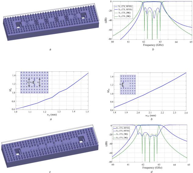
Fig. 7 Structure of the carved groove gap waveguide and its frequency response
(a) Structure of filter with the transitions to WR-15, (b) Calculated and simulated frequency response (with w1 = w5 = 2.96 mm, w2 = w4 = 3.36 mm, w3 = 3.38 mm, w12 = w45 = 3.4 mm, w23 = w34 = 3.07 mm, ds1 = 0.13 mm)
Fig. 8 Realisation of coupling in the iris groove gap waveguide and the TX iris groove gap waveguide filter
(a) Structure of coupling between adjacent cavities and Inter cavity coupling coefficient versus iris width wij, (b) Structure of coupling to the first/last cavity and Input coupling coefficient versus iris width ws1, (c) Structure of the iris filter with the transitions to WR-15, (d) Calculated and simulated frequency response (with w1 = w5 = 2.76 mm, w2 = w4 = 3.0 mm, w3 = 3.06 mm, w12 = w45 = 1.4 mm, w23 = w34 = 1.12 mm, ws1 = 2.14 mm)
5 Groove gap waveguide diplexer: design and fabrication
5.1 Groove gap waveguide diplexer design using iris filter
After separately design of RX and TX iris groove gap waveguide filters, E-plane T-junction, and required transitions to WR-15 flange, the groove gap waveguide diplexer can be realised by connecting these parts as shown in Fig. 9a. It should be noted that a wider bandwidth has been considered in designing of both the RX and TX filters to reduce the impacts of possible frequency shift in filter response due to fabrication errors. As it is seen in Fig. 9a, in order to connect the RX and TX filters to the front-end circuits of the transceiver, two transitions of WR-15 to the groove gap waveguide via the pin plate are used. Also, a transition is used to connect the diplexer to the WR-15 port of the antenna via the cover plate. Due to the loading effect of RX and TX filters on each other after connecting to the T-junction, fine tuning of the diplexer is needed. The simulated frequency response of the optimised diplexer is shown in Fig. 9b which as it can be seen, the desired specifications listed in Table 1 are almost satisfied. The simulated bandwidth of the RX (TX) passband with the return loss better than 16 dB (18 dB) is around 1 GHz (1.5 GHz). Also the minimum insertion loss of the RX and TX passbands are 0.9 and 0.7 dB, respectively. The isolation between two passbands, that is S21 (S31)
at the TX (RX) passband frequency, is better than 55 dB which is near to required isolation listed in Table 1. As it can be seen in Fig. 9b the frequency response slope in the lower edge of RX and TX filters is steep but in the higher edge is slow which is due to excitation of higher order modes of cavities. This soft frequency response and also using wider bandwidth for the filters is the reason of slightly lower isolation than the specification. The simulated group delay of diplexer in the RX and TX bands is depicted in Fig. 9c. As it can be seen, the group delay is almost flat in the RX and TX bandwidths.
5.2 Fabrication of the E-plane groove gap waveguide diplexer and discussion
A prototype of the diplexer is manufactured by using of sawing and milling techniques to validate the design and simulation results. The fabrication process is shown in Fig. 10. The regular pins are manufactured by sawing, horizontally and vertically at first and then, the cavity width, wi and iris size, wij and apertures of
transitions are fabricated by milling. Photograph of the fabricated diplexer after silver plating with thickness of 15 μm is depicted in Fig. 11a. The simulated and measured results of the diplexer are shown in Fig. 11b which an acceptable agreement can be seen. The measured bandwidth with the return loss better than 13.6 dB is around 1.06 and 1.6 GHz for the RX and TX bands, respectively.
IET Microw. Antennas Propag., 2017, Vol. 11 Iss. 15, pp. 2109-2115 |
2113 |
© The Institution of Engineering and Technology 2017 |
|

Fig. 9 E-p/lane groove gap waveguide diplexer
(a) Structure of the diplexer using iris filters, (b) Simulated frequency response of the diplexer (with w1 = w5 = 3.16 mm, w2 = w4 = 3.44 mm, w3 = 3.46 mm, w12 = w45 = 1.42 mm, w23 = w34 = 1.32 mm, ws1 = 2.05 mm for RX filter and w1 = w5 = 2.76 mm, w2 = w4 = 3.0 mm, w3 = 3.06 mm, w12 = w45 = 1.42 mm, w23 = w34 = 1.14 mm, ws1 = 2.14 mm for TX filter), (c) Group delay in RX and TX bands
Fig. 10 Fabrication process of the diplexer
(a) Vertically sawing, (b) Horizontally sawing. Then, the cavities and irises are made by milling technique
The minimum insertion loss of the diplexer at the RX and TX passsbands are 0.9 and 0.8 dB, respectively, and the isolation of two bands is better than 55 dB. As a comparison of the gap waveguide diplexer to an SIW diplexer, the insertion loss of the SIW diplexer presented in [32] is around 7 dB with isolation around 30 dB. In comparison to the conventional rectangular waveguide, the groove gap waveguide is less sensitive to the manufacturing process and presents better agreement between the simulation and measurement results. Moreover, the groove gap waveguide is a robust structure against re-assembling process that makes it a more suitable solution to overcome vibration problems [33]. It should be noted since the gap waveguide structures have more details in the structure, their simulation and optimisation is more time consuming with respect to the conventional waveguide structures.
6 Conclusion
The gap waveguide technology as a promising cost-effective, lowinsertion loss and high-performance platform has found several applications in realisation of millimeter wave devices. In this technology, there is no need for conducting joint between the top
and bottom metal plates. V-band filters and diplexer for radio-link applications realised by using of the groove gap waveguide technology have been presented in this paper. The high-quality factor square groove gap waveguide cavities are used as the filter and diplexer resonators. Coupling matrix approach is used to design of the RX and TX filters. Transitions of the groove gap waveguide to WR-15 input ports of the filter are also designed. E- plane groove gap waveguide T-junction is proposed to connect the diplexer to WR-15 port of the antenna. The presented diplexer is realised by connecting the separately designed RX and TX filters and T-junction. A prototype of the filter and diplexer is manufactured by sawing and milling techniques and an acceptable agreement between simulated and measured results is seen.
7 Acknowledgments
This work was financially supported by the Swedish Governmental Agency for Innovation Systems VINNOVA via a project within the VINN Excellence Center Chase and the European Research Council (ERC) via an advanced investigator grant ERC-2012- ADG_20120216. This work had been started under supervision of the late Prof. Per-Simon Kildal. The authors would like to thank
2114 |
IET Microw. Antennas Propag., 2017, Vol. 11 Iss. 15, pp. 2109-2115 |
|
© The Institution of Engineering and Technology 2017 |

Fig. 11 Photograph of the fabricated diplexer and comparison of the simulated and measured results
(a) Photograph of the diplexer, (b) Simulation and measurement results
Prof. Per-Simon Kildal for being a big source of inspiration to the people working in the antenna group in Chalmers University of technology.
8 References
[1]Vicente, J.C., Hartnagel, H.L.: ‘Passive-intermodulation analysis between rough rectangular waveguide flanges’, IEEE Trans. Microw. Theory Tech., 2005, 53, (8), pp. 2515–2525
[2]Stephens, D., Young, P., Robertson, I.: ‘Millimeter-wave substrate integrated waveguides and filters in photoimageable thick-filmtechnology’, IEEE Trans. Microw. Theory Tech., 2005, 53, (12), pp. 3832–3838
[3]Raza, H., Yang, J., Kildal, P.-S.,, et al.: ‘Microstrip-ridge gap waveguide - study of losses, bends, and transition to WR-15’, IEEE Trans. Microw. Theory Tech., 2014, 62, (9), pp. 1943–1952
[4]Kildal, P.-S., Alfonso, E., Valero-Nogueira, A.,, et al.: ‘Local metamaterialbased waveguides in gaps between parallel metal plates’, IEEE Antennas Wirel. Propag. Lett., 2009, 8, pp. 84–87
[5]Valero-Nogueira, A., Alfonso, E., Herranz, J.I.,, et al.: ‘Experimental demonstration of local quasi-TEM gap modes in single hard-wall waveguides’, IEEE Microw. Wirel. Compon. Lett., 2009, 19, (9), pp. 536–538
[6]Silveirinha, M., Fernandes, C., Costa, J.: ‘Electromagnetic characterization of textured surfaces formed by metallic pins’, IEEE Trans. Antennas Propag., 2008, 56, (2), pp. 405–415
[7]Rajo-Iglesias, E., Kildal, P.-S.: ‘Numerical studies of bandwidth of parallel plate cut-off realized by bed of nails, corrugations and mushroomtype EBG for use in gap waveguides’, IET Microw. Antennas Propag., 2011, 5, (3), pp. 282–289
[8]Kildal, P.S.: ‘Three metamaterial-based gap waveguides between parallel metal plates for mm/submm waves’. 3rd European Conf. on Antennas and Propagation, EuCAP, 2009, pp. 28–32
[9]Kildal, P.-S., Zaman, A., Rajo-Iglesias, E.,, et al.: ‘Design and experimental verification of ridge gap waveguide in bed of nails for parallel-plate mode suppression’, IET Microw. Antennas Propag., 2011, 5, (3), pp. 262–270
[10]Polemi, A., Maci, S., Kildal, P.S.: ‘Dispersion characteristics of a metamaterial-based parallel-plate ridge gap waveguide realized by bed of nails’, IEEE Trans. Antennas Propag., 2011, 59, (3), pp. 904–913
[11]Pucci, E., Zaman, A., Rajo-Iglesias, E.,, et al.: ‘Study of Q-factors of ridge and groove gap waveguide resonators’, IET Microw. Antennas Propag., 2013, 7, (11), pp. 900–908
[12]Raza, H., Yang, J., Kildal, P.-S.,, et al.: ‘Resemblance between gap waveguides and hollow waveguides’, IET Microw. Antennas Propag., 2013, 7, (15), pp. 1221–1227
[13]Razavi, S.A., Kildal, P.-S., Xiang, L.,, et al.: ‘2 × 2-slot element for 60 GHz planar array antenna realized on two doubled-sided PCBs using SIW cavity and EBG-type soft surface fed by microstrip-ridge gap waveguide’, IEEE Trans. Antennas Propag., 2014, 62, (9), pp. 4564–4573
[14]Zaman, A.U., Kildal, P.S.: ‘Wide-band slot antenna arrays with single-layer corporate-feed network in ridge gap waveguide technology’, IEEE Trans. Antennas Propag., 2014, 62, pp. 2992–3001
[15]Al Sharkawy, M., Kishk, A.A.: ‘Long slots array antenna based on ridge gap waveguide technology’, IEEE Trans. Antennas Propag., 2014, 62, pp. 5399– 5403
[16]Zarifi, D., Farahbakhsh, A., Zaman, A.U.,, et al.: ‘Design and fabrication of a high-gain 60-GHz corrugated slot antenna array with ridge gap waveguide
distribution layer’, IEEE Trans. Antennas Propag., 2016, 64, (7), pp. 2905– 2913
[17]Alfonso, E., Zaman, A.U., Kildal, P.-S.: ‘Ka-band gap waveguide coupledresonator filter for radio link diplexer application’, IEEE Trans. Compon. Packag. Manuf. Technol., 2013, 3, (5), pp. 870–879
[18]Ahmadi, B., Banai, A.: ‘Direct coupled resonator filters realized by gap waveguide technology’, IEEE Trans. Microw. Theory Tech., 2015, 63, (10),
pp.3445–3452
[19]Zaman, A., Kildal, P.-S., Kishk, A.A.: ‘Narrow-band microwave filter using high-Q groove gap waveguide resonators with manufacturing flexibility and no sidewalls’, IEEE Trans. Compon. Packag. Manuf. Technol., 2012, 2, (11),
pp.1882–1889
[20]Sharifi, M., Khaleghi, A., Kildal, P.-S.: ‘Direct-coupled cavity filter in ridge gap waveguide’, IEEE Trans. Compon. Packag. Manuf. Technol., 2014, 4, (3),
pp.490–495
[21]Rezaee, M., Zaman, A.U., Kildal, P.S.: ‘Groove gap waveguide iris filter for V-band application’. 23th Iranian Conf. on Electrical Engineering, ICEE, 2015, pp. 462–465
[22]Alfonso, E., Zaman, A.U., Pucci, E.,, et al.: ‘Gap waveguide components for millimetre-wave systems: couplers, filters, antennas, MMIC packaging’. ISAP, Nagoya, Japan, 2012, pp. 243–246
[23]Molaei, B., Khaleghi, A.: ‘A novel wideband microstrip line to ridge gap waveguide transition using defected ground slot’, IEEE Microw. Wirel. Comp. Lett., 2015, 25, (2), pp. 91–93
[24]Farahbakhsh, A., Zarifi, D., Zaman, A.U.: ‘60-GHz groove gap waveguide based wideband H-plane power dividers and transitions: for use in high-gain slot array antenna’, IEEE Trans. Microw. Theory Tech., DOI: 10.1109/ TMTT.2017.2699680
[25]Zaman, A.U., Vukusic, T., Alexanderson, M.,, et al.: ‘Gap waveguide PMC packaging for improved isolation of circuit components in high frequency microwave modules’, IEEE Trans. Compon. Packag. Manuf. Technol., 2014,
4, (1), pp. 16–25
[26]Brazález, A., Zaman, A.U., Kildal, P.-S.: ‘Improved microstrip filters using PMC packaging by lid of nails’, IEEE Trans. Compon., Packag. Manuf. Technol., 2012, 2, (7), pp. 1075–1084
[27]Dittloff, J., Arndt, F.: ‘Computer-aided design of slit-coupled H-plane T- junction diplexers with E-plane metal-insert filters’, IEEE Trans. Microw. Theory Tech., 1988, 36, (12), pp. 1833–1840
[28]Ofli, E., Vahldieck, R., Amari, S.: ‘Novel E-plane filters and diplexers with elliptic response for millimeter-wave applications’, IEEE Trans. Microw. Theory Tech., 2005, 53, (3), pp. 843–851
[29]Rezaee, M., Zaman, A.U., Kildal, P.S.: ‘V-band groove gap waveguide diplexer’. 9th European Conf. on Antennas and Propagation, EuCAP, 2015
[30]Cameron, R.J., Kudsia, C.M., Mansour, R.R.: ‘Microwave filters for communication systems: fundamentals, design, and applications’ (John Wiley & Sons, 2007)
[31]Berenguer, A., Fusco, V., Zelenchuk, D.E.,, et al.: ‘Propagation characteristics of groove gap waveguide below and above cutoff’, IEEE Trans. Microw. Theory Tech., 2016, 64, (1), pp. 27–36
[32]Wang, D., Chin, K., Che, W.,, et al.: ‘60 GHz duplexer design using dualmode SIW filters with single-sided transmission zeros’, Electron. Lett., 2014, 50, (21), pp. 1529–1531
[33]Berenguer, A., Sánchez-Escuderos, D., Bernardo-Clemente, B.,, et al.: ‘Groove gap waveguide as an alternative to rectangular waveguide for H- plane components’, Electron. Lett., 2016, 52, (11), pp. 939–941
IET Microw. Antennas Propag., 2017, Vol. 11 Iss. 15, pp. 2109-2115 |
2115 |
© The Institution of Engineering and Technology 2017 |
|