

диафрагмированные волноводные фильтры / 1c50c064-e817-42ce-b541-31677475b7dc
.pdfThis article has been accepted for inclusion in a future issue of this journal. Content is final as presented, with the exception of pagination.
IEEE TRANSACTIONS ON MICROWAVE THEORY AND TECHNIQUES |
1 |
A Miniaturized Evanescent Mode Waveguide
Filter Using RRRs
Jun Ye Jin, Student Member, IEEE, Xian Qi Lin, Senior Member, IEEE, and Quan Xue, Fellow, IEEE
Abstract— In this paper, a miniaturized evanescent mode waveguide filter using rectangular ring resonators (RRRs) is presented. The evanescent mode waveguide resonator cell (EWRC), composed of a section of evanescent mode waveguide loaded with a pair of RRRs, is designed and analyzed. Quality factors of the EWRC are simulated and calculated. The resonant mechanism and the values of the equivalent lumped elements of EWRCs are given for further design and application of this kind of filter. A miniaturized waveguide filter is designed and fabricated to operate at Ka-band, using the W-band standard waveguide (WR-10) with a cross-sectional size of 2.54 mm × 1.27 mm. The proposed filter can realize a large size reduction compared with the conventional waveguide filter, especially leading to a cross-sectional size reduction of 87.2%. Despite a slight frequency shift, good agreement has been achieved between the simulation and measurement results. The proposed filter has large out-of-band rejection, wide stopband, and high selectivity. In addition, a compact diplexer with high isolation is presented.
Index Terms— Compact size, diplexer, E-plane, evanescent mode, Ka-band, waveguide filter.
I. INTRODUCTION
OVER the past decades, the waveguide has been an indispensable solution to design robust, low loss, and high-power filters [1]–[4] at microwave and millimeterwave frequencies. With the development of microwave and millimeter-wave systems, high-performance narrow-band bandpass filters with low insertion loss, compact size, wide stopband, and high selectivity are increasingly required. In the design of waveguide filter structures, reduction of the physical size and weight has become one of the primary goals. In order to realize miniaturization, most waveguide filters focused on reducing the total length of waveguide filter [5]–[7], by using compact resonators or dual-mode cavities [8], [9]. However, except of waveguide filters, the
Manuscript received November 10, 2015; revised May 19, 2016; accepted May 28, 2016. This work was supported in part by the National key Basic Research Program of the Ministry of Science and Technology of China (973 Program) under Grant 2014CB339900, in part by the National Natural Science Foundation of China under Grant 61372056 and Grant 61571084, in part by NCET under Grant NCET-13-0095, and in part by FRF for CU under Grant ZYGX2014J016.
J. Y. Jin and Q. Xue are with the State Key Laboratory of Millimeter Waves, Department of Electronic Engineering, City University of Hong Kong, Hong Kong, and also with the Shenzhen Key Laboratory of Millimeter Waves, CityU Shenzhen Research Institute, Shenzhen 518057, China (e-mail: junyejin2- c@my.cityu.edu.hk; eeqxue@cityu.edu.hk).
X. Q. Lin is with the EHF Key Laboratory of Fundamental Science, School of Electronic Engineering, University of Electronic Science and Technology of China, Chengdu 611731, China (e-mail: xqlin@uestc.edu.cn).
Color versions of one or more of the figures in this paper are available online at http://ieeexplore.ieee.org.
Digital Object Identifier 10.1109/TMTT.2016.2574988
sizes of cross section should also be considered in order to design compact waveguide filters. The evanescent mode waveguide filter [10]–[13] has been a suitable choice to realize this goal. The evanescent mode bandpass filters have several advantages over the conventional type of bandpass filter (waveguide used above cutoff frequency). On the one hand, larger out-of-band rejection can be obtained. On the other hand, evanescent mode waveguide filters own the advantages in both volume and weight compared with traditional waveguide. However, evanescent mode filters using conventional capacitive elements such as tuning screws [11], [12] are costly and difficult to mass-produce because of their complicated structure. In addition, the tuning screws limit the sizes of evanescent mode waveguide and they are not applicable at higher frequencies. Besides, transverse inserts used in the designed evanescent mode waveguide filters made the fabrication more expensive and complex [10], [14]. In order to implement easy fabrication, mass production, and low cost, the nontouching E-plane fins [13] were proposed as the capacitive elements to design the evanescent mode filters operating at Ka-band. The height of the fins must be smaller than the height of the evanescent mode waveguide. An evanescent mode waveguide filter with two E-plane fins on a Duroid substrate was simulated and given in [13, Fig. 14], which had a center frequency of about 30.5 GHz and 3 dB bandwidth of 5%. The larger waveguide and the smaller waveguide were WR-28 (7.11 mm × 3.56 mm) and WR-15 (3.76 mm × 1.88 mm), respectively, leading to a cross size reduction of 72%.
The equivalent capacitors were emphasized and considered in designing the conventional evanescent mode waveguide filters and the design theory was also based on the termination in capacitors. However, the equivalent inductance also plays an important role in the filter performance. It should be studied for potential design and application. Moreover, most of the previous works designed the evanescent mode waveguide filter with nonstandard cross section sizes, which caused measurement complexity or need of the input and output (I/O) ports of suitable waveguide. Such as in the work of [15], the revealed passband below the cutoff frequency had a large measured transmission loss of more than 30 dB.
In this paper, a miniaturized evanescent mode waveguide filter is presented to operate at Ka-band and a cross size reduction of 87.2% is achieved by using WR-10. The resonances of rectangular ring resonators (RRRs) in evanescent mode waveguide are appropriately used. The effect of equivalent
inductance is fully considered as well as the |
capacitance. |
At the meantime, this filter has good features |
of low cost |
0018-9480 © 2016 IEEE. Personal use is permitted, but republication/redistribution requires IEEE permission. See http://www.ieee.org/publications_standards/publications/rights/index.html for more information.

This article has been accepted for inclusion in a future issue of this journal. Content is final as presented, with the exception of pagination.
2 |
|
|
|
|
|
|
|
|
|
|
|
|
|
|
|
|
|
|
|
|
|
|
|
IEEE TRANSACTIONS ON MICROWAVE THEORY AND TECHNIQUES |
||||||||||||||||||||||||||||||
|
|
|
|
|
|
|
|
|
|
|
|
|
|
|
|
|
|
|
|
|
|
|
|
|
|
|
|
|
|
|
|
|
|
|
|
|
|
|
|
|
|
|
|
|
|
|
|
|
|
|
|
|
|
|
|
|
|
|
|
|
|
|
|
|
|
|
|
|
|
|
|
|
|
|
|
|
|
|
|
|
|
|
|
|
|
|
|
|
|
|
|
|
|
|
|
|
|
|
|
|
|
|
|
|
|
|
|
|
|
|
|
|
|
|
|
|
|
|
|
|
|
|
|
|
|
|
|
|
|
|
|
|
|
|
|
|
|
|
|
|
|
|
|
|
|
|
|
|
|
|
|
|
|
|
|
|
|
|
|
|
|
|
|
|
|
|
|
|
|
|
|
|
|
|
|
|
|
|
|
|
|
|
|
|
|
|
|
|
|
|
|
|
|
|
|
|
|
|
|
|
|
|
|
|
|
|
|
|
|
|
|
|
|
|
|
|
|
|
|
|
|
|
|
|
|
|
|
|
|
|
|
|
|
|
|
|
|
|
|
|
|
|
|
|
|
|
|
|
|
|
|
|
|
|
|
|
|
|
|
|
|
|
|
|
|
|
|
|
|
|
|
|
|
|
|
|
|
|
|
|
|
|
|
|
|
|
|
|
|
|
|
|
|
|
|
|
|
|
|
|
|
|
|
|
|
|
|
|
|
|
|
|
|
|
|
|
|
|
|
|
|
|
|
|
|
|
|
|
|
|
|
|
|
|
|
|
|
|
|
|
|
|
|
|
|
|
|
|
|
|
|
|
|
|
|
|
|
|
|
|
|
|
|
|
|
|
|
|
|
|
|
|
|
|
|
|
|
|
|
|
|
|
|
|
|
|
|
|
|
|
|
|
|
|
|
|
|
|
|
|
|
|
|
|
|
|
|
|
|
|
|
|
|
|
|
|
|
|
|
|
|
|
|
|
|
|
|
|
|
|
|
|
|
|
|
|
|
|
|
|
|
|
|
|
|
|
|
|
|
|
|
|
|
|
|
|
|
|
|
|
|
|
|
|
|
|
|
|
|
|
|
|
|
|
|
|
|
|
|
|
|
|
|
|
|
|
|
|
|
|
|
|
|
|
|
|
|
|
|
|
|
|
|
|
|
|
|
|
|
|
|
|
|
|
|
|
|
|
|
|
|
|
|
|
|
|
|
|
|
|
|
|
|
|
|
|
|
|
|
|
|
|
|
|
|
|
|
|
|
|
|
|
|
|
|
|
|
|
|
|
|
|
|
|
|
|
|
|
|
|
|
|
|
|
|
|
|
|
|
|
|
|
|
|
|
|
|
|
|
|
|
|
|
|
|
|
|
|
|
|
|
|
|
|
|
|
|
|
|
|
|
|
|
|
|
|
|
|
|
|
|
|
|
|
|
|
|
|
|
|
|
|
|
|
|
|
|
|
|
|
|
|
|
|
|
|
|
|
|
|
|
|
|
|
|
|
|
|
|
|
|
|
|
|
|
|
|
|
|
|
|
|
|
|
|
|
|
|
|
|
|
|
|
|
|
|
|
|
|
|
|
|
|
|
|
|
|
|
|
|
|
|
|
|
|
|
|
|
|
|
|
|
|
|
|
|
|
|
|
|
|
|
|
|
|
|
|
|
|
|
|
|
|
|
|
|
|
|
|
|
|
|
|
|
|
|
|
|
|
|
|
|
|
|
|
|
|
|
|
|
|
|
|
|
|
|
|
|
|
|
|
|
|
|
|
|
|
|
|
|
|
|
|
|
|
|
|
|
|
|
|
|
|
|
|
|
|
|
|
|
|
|
|
|
|
|
|
|
|
|
|
|
|
|
|
|
|
|
|
|
|
|
|
|
|
|
|
|
|
|
|
|
|
|
|
|
|
|
|
|
|
|
|
|
|
|
|
|
|
|
|
|
|
|
|
|
|
|
|
|
|
|
|
|
|
|
|
|
|
|
|
|
|
|
|
|
|
|
|
|
|
|
|
|
|
|
|
|
|
|
|
|
|
|
|
|
|
|
|
|
|
|
|
|
|
|
|
|
|
|
|
|
|
|
|
|
|
|
|
|
|
|
|
|
|
|
|
|
|
|
|
|
|
|
|
|
|
|
|
|
|
|
|
|
|
|
|
|
|
|
|
|
|
|
|
|
|
|
|
|
|
|
|
|
|
|
|
|
|
|
|
|
|
|
|
|
|
|
|
|
|
|
|
|
|
|
|
|
|
Fig. 2. Simulation results of WR-10 loaded with the RRRs and
SRRs (g = 0.1 mm).
Fig. 1. Proposed EWRC. (a) Side view. (b) Top view. (c) Simulation results of the EWRC versus l (with h = 1.1 mm and t = 0.1 mm).
Fig. 3. Simulation results of WR-10 loaded with the RRRs and SRRs (h = 1.1 mm, l = 1.6 mm, lsrr = 0.75 mm, g = 0.2 mm, and t = 0.1 mm).
and easy fabrication. The basic theory and design analysis are presented in Section II, including equivalent circuit analysis in which the lumped elements are given in closed formulas. One sample is designed, fabricated, and measured in Section III. A compact diplexer with high isolation is further proposed based on the proposed filter design in Section IV. Finally, some necessary conclusions are drawn in Section V.
II. BASIC DESIGN THEORY
It is well known that the W -band standard waveguide WR-10 with 2.54 mm × 1.27 mm is always used to transmit the W -band electromagnetic wave ranging from 75 to 110 GHz, but cannot transmit the Ka-band wave ranging from 26.5 to 40 GHz. Therefore, when a WR-10 is directly connected with the I/O ports of WR-28 with the crosssectional sizes of 7.112 mm × 3.556 mm, the evanescent mode waveguide of WR-10 definitely reflects all the Ka-band electromagnetic wave [16].
A. Evanescent Mode Waveguide Resonator Cell
Here, first, the evanescent mode waveguide resonator cell (EWRC) is designed using the WR-10 and RRRs, operating at Ka-band. A pair of identical RRRs, which are placed back-to-back and supported by a Duroid substrate with the relative permittivity of εr = 2.2 and the thickness of 0.127 mm, is inserted in the center E-plane of the WR-10, as shown in Fig. 1. For extremely compact sizes, the evanescent mode waveguide is fully used by the rectangular ring with
h = 1.1 mm, and h is limited by the narrow wall of the WR-10. A passband is produced at its resonant frequency, which is designed to locate in the Ka-band, as shown in Fig. 1(c). The operating frequency of the EWRC can be adjusted by the size parameters of RRRs.
It should be mentioned that split ring resonators (SRRs) is also evaluated, but the obtained results show that the RRRs have a superior performance. In Fig. 2, for the SRRs with the same parameters of l and h of the RRRs, except for a gap with g = 0.1 mm, two resonant modes are observed. The first transmission pole is introduced by a magnetic resonance at a lower frequency, while the second one is induced at a higher frequency by an electric resonance whose current distribution is symmetrical with respect to the center line. Because the waveguide field is electrically coupled to the resonators, the electric resonance plays a more important role than the magnetic resonance. It can be seen that the dominant electric resonant mode has better transmission performance than the magnetic resonant mode. Thus, on the one hand, the magnetic mode is companied by large insertion loss and narrow passband, and it should be suppressed for designing a bandpass filter with a better out-of-band rejection in the lower stopband. On the other hand, the electric resonant mode with lower insertion loss and wider passband is similar to that of the proposed EWRC which realizes magnetic mode suppression.
In Fig. 3, the split of SRR is perpendicular to the waveguide longitudinal axis. In this case, only the magnetic resonant mode is excited, as shown in the inset of Fig. 3, while the

This article has been accepted for inclusion in a future issue of this journal. Content is final as presented, with the exception of pagination.
JIN et al.: MINIATURIZED EVANESCENT MODE WAVEGUIDE FILTER USING RRRs |
3 |
|||||||||||||||||||
|
|
|
|
|
|
|
|
|
|
|
|
|
|
|
|
|
|
|
|
|
|
|
|
|
|
|
|
|
|
|
|
|
|
|
|
|
|
|
|
|
|
|
|
|
|
|
|
|
|
|
|
|
|
|
|
|
|
|
|
|
|
|
|
|
|
|
|
|
|
|
|
|
|
|
|
|
|
|
|
|
|
|
|
|
|
|
|
|
|
|
|
|
|
|
|
|
|
|
|
|
|
|
|
|
|
|
|
|
|
|
|
|
|
|
|
|
|
|
|
|
|
|
|
|
|
|
|
|
|
|
|
|
|
|
|
|
|
|
|
|
|
|
|
|
|
|
|
|
|
|
|
|
|
|
|
|
|
|
|
|
|
|
|
|
|
|
|
Fig. 5. Parallel LC equivalent circuit of waveguide loaded with the RRRs.
(a) Including impedance scaling. (b) Excluding for impedance scaling.
Fig. 4. Evanescent mode waveguide filter. (a) Qu of EWRC.
(b) Qe of EWRC.
electric resonance cannot be induced. So the field coupling of SRRs is much weaker than that of the RRRs and the insertion loss is much higher. So considering all the above discussions, the RRRs are preferred.
B. Quality Factors of EWRC
The relationship between the loaded quality factor (Ql ), unloaded quality factor (Qu ), and external quality factor (Qe) is determined by
|
1 |
= |
1 |
|
+ |
1 |
. |
(1) |
|
Ql |
Qu |
Qe |
|||||
Then, the unloaded |
quality |
factor (Qu ) of |
the EWRC |
|||||
is investigated, which is determined by its corresponding
section |
waveguide, supported |
substrate |
(dielectric loss of |
|||
tan δ |
= |
9 |
× |
7 |
metallic |
RRRs [copper with |
|
|
10−4), and the |
||||
conductivity of σ = 5.8 × 10 (S/m)]. By enlarging the length of evanescent mode waveguide at the I/O ports, i.e., lew, to reduce the I/O couplings to the EWRC (until S21 < −20 dB and Qe is approximately infinite), as shown in Fig. 4(a), Qu is simulated and calculated by
Qu ≈ Ql = |
1 |
(2) |
FBW |
where FBW is the fractional 3 dB bandwidth. Here, Qu of EWRC with h = 1.1 mm and l = 1.6 mm is 778. Because of its structure, this Qu should be lower than Qu of metallic cavity, but higher than the microstrip resonators. A high Qu is obtained by our proposed EWRC.
By reducing the I/O couplings to the EWRC, the unloaded Qu can be calculated. In contrast, by increasing the couplings, the external quality factor (Qe) is obtained by (2), similarly. Moreover, as the bandwidth of filters related to Qe directly, it is investigated. As shown in Fig. 4(b), lew is the same as in Fig. 4(a), while lsw means the length that the RRRs protrude into the standard waveguide of WR-28. Qe of EWRC with lew = lsw = 0 is 23.6. As shown in Fig. 4(b), Qe is reduced to 20 when the RRRs protrude into the standard waveguide, which can be used to design filter with a wider bandwidth. On the other hand, Qe is increased to 27.3, when there is a section of evanescent mode waveguide at the I/O ports.
However, considering the practical fabrication, it is not good to have the RRRs extended out its evanescent mode waveguide, because the substrate circuit is easy to be damaged. Moreover, if we only fabricate the filter structures, the extended substrate and the metallic structure on it makes inconvenient for resembling and measurement. Therefore, it is better for us to allocate the substrate circuit into the waveguide. Much narrower bandwidth filters can be designed by adjusting lew. But, in this design, we focus on the designs with lew = 0 mm for a filter with minimum length.
C. Equivalent Circuit Analysis
The EWRC, a WR-10 loaded with a pair of identical RRRs in Fig. 1, can be equivalent to a parallel LC circuit, as shown in Fig. 5(a), where L and C are the equivalent inductance and capacitor. Further, let Ln and Cn are the equivalent inductance and capacitor before impedance scaling, as shown in Fig. 5(b), so they are determined by
Ln = |
L |
|
(3) |
Z0 |
|||
Cn = C Z0 |
(4) |
||
where Z0 is the characteristic impedance of the I/O WR-28 and Z0 can be calculated by
Z0 |
|
K |
b1 |
|
|
μ0 |
|
1 |
|
|
|
|
(5) |
||
|
|
|
|
|
|
|
|
|
|||||||
|
= |
· a1 |
|
|
ε0 |
|
1 − |
2a01 |
|
2 |
|
|
|||
|
|
|
|
|
|
λ |
|
|
|
||||||
|
|
|
|
|
|
|
|
|
|
|
|
|
|
|
|
where a1, b1, μ0, ε0, and λ0 are waveguide wide dimension, waveguide narrow dimension, permeability, permittivity of the I/O waveguide WR-28, and free space wavelength, respectively, and K is a coefficient which equals 2 for Z0 calculated from power and voltage at the center of broadside wall. The calculated results of Z0 using (5) are shown in Fig. 6 for further design in Section III. From Fig. 6, it can be seen that Z0 varies as the frequency changes. The resonant frequency f0, however, only determines the product of L and C,

This article has been accepted for inclusion in a future issue of this journal. Content is final as presented, with the exception of pagination.
4 |
|
|
IEEE TRANSACTIONS ON MICROWAVE THEORY AND TECHNIQUES |
|||||||||
|
|
|
|
|
|
|
|
|
|
|
|
|
|
|
|
|
|
|
|
|
|
|
|
|
|
|
|
|
|
|
|
|
|
|
|
|
|
|
|
|
|
|
|
|
|
|
|
|
|
|
|
|
|
|
|
|
|
|
|
|
|
|
|
|
|
|
|
|
|
|
|
|
|
|
|
|
|
|
|
|
|
|
|
|
|
|
|
|
|
|
|
|
|
|
|
|
|
|
|
|
|
|
|
|
|
|
|
|
|
|
|
|
|
|
|
|
|
|
|
|
|
|
|
|
|
|
|
|
|
|
|
|
|
|
|
|
|
|
|
|
|
|
Fig. 6. Characteristic impedance Z0 of WR-28.
Fig. 8. Comparisons of the equivalent LC circuit and the evanescent mode cell.
Fig. 7. f0 versus the length of RRRs.
or the product of Ln and Cn , i.e., LC = Ln Cn = 1/ω02, where ω0 = 2π f0 is the angular frequency at the resonant frequency f0 of the EWRC. By carefully investigation of the EWRC, it can be found that Cn increases when increasing l, and the larger h leads to smaller Cn. Moreover, Cn depends on Ln , so we can only focus on the investigation of Ln . The parameters of h and l determine the resonant frequency f0, while fixing the width of metal strip (t = 0.1 mm), as shown in Fig. 7. Smaller value of l results in higher resonant frequency. The relationship between Ln and the sizes of the RRRs is carefully analyzed here. It can be simply determined by
Ln = [0.37 − 0.1(l + h)] × 10−3 nH. |
(6) |
A comparison of simulation results of the equivalent LC circuit and the EWRC is shown in Fig. 8, which selects EWRC with t = 0.1 mm, h = 1.1 mm, and l = 1.6 mm. The resonant frequency is 31.6 GHz, at which the value of Z0 is 505.8 . Ln is calculated using (6) to be 0.1 × 10⁻³ nH, so L is then determined by (3) to be 0.05058 nH, and then C is 0.5023 pF as shown in the inset of Fig. 8. Slight differences are observed far from the center frequency, because the substrate and EWRC are along the direction of wave propagation. Different phases of electromagnetic field are presented at two edges of the structures, So the out-of-band rejection performance is not symmetrical about the center frequency.
III. FILTER DESIGN AND EXPERIMENT
Fig. 9. Equivalent LC circuit of the proposed filter. Two cells with (a) length of waveguide, (b) with π -network, and (c) using J-inverter.
represented by the equivalent LC circuit and a length of evanescent mode waveguide, as shown in Fig. 9(a). For the TE evanescent modes, a section of evanescent mode waveguide with le equals a T- or π -network represented by lumped reactance components [17] and the π -network is used in Fig. 9(b). When the evanescent mode waveguide is air-filled, the reactance Z1 and Z2 can be calculated by
Z1 = j |
|
|
120π b2 |
|
|
|
sinh γ le |
(7) |
|||||||
|
|
|
|
|
|
|
|
|
|||||||
a2 |
|
2 |
|
|
|
||||||||||
|
|
2a02 |
− 1 |
|
|
|
|
||||||||
|
|
|
|
|
|
λ |
|
|
|
|
|
|
|
|
|
Z2 = j |
|
|
120π b2 |
|
|
|
coth |
γ le |
(8) |
||||||
|
|
|
|
|
|
|
|
|
|
||||||
|
|
|
|
|
|
|
|
|
2 |
||||||
a2 |
|
2 |
|
|
|
||||||||||
|
|
2a02 |
− 1 |
|
|
|
|
||||||||
|
|
|
|
|
|
λ |
|
|
|
|
|
|
|
|
|
where the propagation constant γ is given by |
|
||||||||||||||
|
|
|
|
|
|
|
|
|
|
|
|
|
|
|
|
γ |
= |
|
2π |
|
λ0 |
|
2 |
− |
1. |
|
(9) |
||||
|
|
2a2 |
|
|
|||||||||||
|
|
λ0 |
|
|
|
|
|
|
|||||||
Using the proposed EWRC as a filter cell, it is possible to design a miniaturized evanescent mode waveguide bandpass filter. The schematic graph of the cascaded cells is
A J-inverter, formed by this section of evanescent mode waveguide, is employed to analyze the proposed evanescent mode filter, as shown in Fig. 9(c). This J-inverter is used
This article has been accepted for inclusion in a future issue of this journal. Content is final as presented, with the exception of pagination.
JIN et al.: MINIATURIZED EVANESCENT MODE WAVEGUIDE FILTER USING RRRs |
5 |
|||
|
|
|
|
|
|
|
|
|
|
|
|
|
|
|
|
|
|
|
|
|
|
|
|
|
Fig. 11. Calculated f versus le .
Fig. 10. Proposed evanescent mode waveguide filter structures.
to couple the two EWRCs, resulting in a bandpass filter. From Fig. 9(c), it can be seen that the reactance of Zt , i.e., Zt = Z1 + Z2, can shift the original resonant frequency f0 of the EWRCs to higher frequencies. In addition, this frequency shift f can be calculated by
|
f |
= |
f |
− |
f |
|
= |
1 |
|
|
1 |
|
|
|
1 |
|
(10) |
||
0 |
|
|
|
|
|
|
− √ |
|
|||||||||||
|
|
|
2π |
|
|
LL LL |
C |
LC |
|
|
|||||||||
|
|
|
|
|
|
|
|
|
|
|
|
|
|
|
|
|
|
|
|
|
|
|
|
|
|
|
|
|
+ |
|
|
|
|
|
|
|
|||
where f is the center frequency of the proposed filter, and L is the equivalent inductance of Zt . Zt and L are determined by
Zt = Z1 + Z2 = j |
|
120π b2 |
|
|
tanh γ le (11) |
|||||
|
|
|
|
|
|
|
||||
a2 |
|
|
2 |
|
|
|||||
|
|
|
2a02 |
− 1 |
||||||
|
|
|
|
|
|
λ |
|
|
|
|
L = |
Zt |
|
|
|
|
(12) |
||||
|
H. |
|
|
|
|
|||||
jw |
|
|
|
|
||||||
Using the HFSS software, the simulation model of the proposed filter is shown in Fig. 10, where two EWRCs are placed at appropriate interval of d and the I/O ports of WR-28 are modeled for exact simulation. It should be noted that d should be larger than le, because the RRRs of the EWRCs introduce fringing fields into the evanescent mode waveguide section. Following steps should be taken as the design procedures in this paper.
Step 1: According to the operating center frequency of the required to determine the center frequency f0 of the EWRC, and then to get the sizes of the EWRC by Fig. 7.
Step 2: Calculate Ln using (6) and Cn from the relationship
with Ln (LnCn = 1/ω02).
Step 3: Calculate the characteristic impedance Z0 using (5) or obtain it by Fig. 6, and then, get L and C.
Step 4: Simulation verification and fine optimization to determine the required value of d.
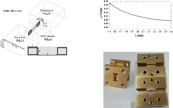
To demonstrate this design method, a sample was designed and fabricated. The EWRCs with h = 1.1 mm and l = 1.66 mm are chosen, which resonate at 31 GHz. So the parameters are Ln = 0.094 × 10⁻³ nH,Cn = 278.8 pF, Z0 = 513.7 , L = 0.048 nH, and C = 0.5427 pF. Moreover, the value of f is calculated using (10) at 31 GHz versus the length of le, as shown in Fig. 11. It can be seen that a frequency shift of more than 1.2 GHz is induced for a section of
Fig. 12. Photograph of the proposed evanescent mode waveguide filter.
air-filled evanescent mode waveguide theoretically. Considering the difference between the ideal lumped components and the realistic structures with losses, the discrepancy between the air-filled waveguide and the substrate inserted waveguide, and existence of fringing fields, this frequency deviation may be larger than the calculated one.
A photograph of the filter is shown in Fig. 12. This sample of the proposed miniaturized evanescent mode filter is tested by the PNA Network Analyzer N5244A. The RRRs are fabricated on the Duroid 5880 substrate with the relative permittivity of εr = 2.2 and the thickness of 0.127 mm which is inserted in the center E-plane of the standard WR-10. The I/O ports are the standard waveguides of WR-28. It should be mentioned that this kind of waveguide filter can be realized by fabricating an RRRs-loaded W -band waveguide with the Ka-band flange, which is used to connect with the I/O ports of WR-28. However, in the experiment, the total length of the proposed filter with l = 1.66 mm and d = 2.54 mm is 5.9 mm, which is too short to assemble to the experiment equipment, so the extra lengths of the I/O ports are fabricated together with the filter, as shown in Fig. 12, for easy assembling and test.
The step-discontinuity effect at the boundary between the evanescent-mode waveguide and the input standard waveguide is included in the design procedures and the measurement results. Comparisons between the simulation and measurement results are shown in Fig. 13. The simulation and measurement results show that the waveguide filter has large out-of-band rejection and high selectivity. The steepness of the out-of-band insertion loss curve on the higher frequency side is almost equal to the one on the lower frequency side. This happens because the waveguide below its cutoff frequency acts

This article has been accepted for inclusion in a future issue of this journal. Content is final as presented, with the exception of pagination.
6
Fig. 13. Comparison between HFSS simulation and measurement results (with l = 1.66 mm, h = 1.1 mm, t = 0.1 mm, and d = 2.54 mm).
TABLE I
COMPARISON WITH REPORTED RESEARCH
like a lumped reactance, contributing to large rejection. The HFSS simulated sample operates at the center frequency of 32.8 GHz with a 3 dB bandwidth of 3%, whereas the measured one works at the center frequency of 32.3 GHz with a 3 dB bandwidth of 3%. It is noted that the center frequency of the designed filter is higher than the resonant frequency of the EWRCs. The measured minimum insertion loss is 0.86 dB and the skirt coefficient of K0.1 is calculated to be 1.83. Finally, a frequency shift of 0.5 GHz (1.5%) between the HFSS simulation and measurement results is shown, which is mainly because of the fabrication tolerance, resembling, and material errors. Despite the slight frequency shift, good agreement is achieved between the simulation and measurement results. Besides, there is no doubt that the proposed filter can operate exactly at any other central frequencies by changing the sizes of the RRRs, i.e., l and h.
Some comparisons have been summarized between a previous waveguide filter operating at Ka-band and ours as shown in Table I. This kind of proposed filter can realize a very large size reduction compared with the conventional waveguide filter. The cross section size of this proposed one is 2.54 mm × 1.27 mm, which is only 12.8% of that of the conventional ones, which are always 7.112 mm × 3.556 mm, such as the filter in [18]. The proposed filter is not only smaller than the previous waveguide filters in length, but also with smaller cross section sizes.
IV. DIPLEXER DESIGN
As shown earlier, this kind of waveguide filter with compact size has a larger out-of-band rejection, so it can be used to design a compact diplexer. In this section, a compact diplexer would be proposed using the described evanescent
IEEE TRANSACTIONS ON MICROWAVE THEORY AND TECHNIQUES
Fig. 14. |
Simulation results of Filter1 and Filter2 (with l1 = l2 = 1.8 mm, |
t1 = t2 |
= 0.1 mm, h1 = 1.1 mm, h2 = 1 mm, d1 = 2.5 mm, and |
d2 = 2.6 mm).
Fig. 15. Configuration of the compact diplexer.
mode waveguide filter. First of all, two filters (denoted by Filter1 and Filter2) operate at different frequency bands need to be selected. Here, Filter1 (h1 = 1.1 mm, l1 = 1.8 mm, t1 = 0.1 mm, and d1 = 2.5 mm) and Filter2 (h2 = 1.0 mm, l2 = 1.8 mm, t2 = 0.1 mm, and d2 = 2.6 mm) are chosen for the next step. The simulation results of the two filters are shown in Fig. 14. Filter1 operates at 31.86 GHz with a 3 dB bandwidth of 3%, whereas Filter2 operates at 35.82 GHz with a 3 dB bandwidth of 3.1%. These two filters are used in two channels of the diplexer separately for different works.
For easy fabrication, the conventional T-junction is utilized, as shown in Fig. 15. The two filters are located at two arms of
the T-junction of |
this designed diplexer. The parameters |
of dcen1 and dcen2 |
represent the distances from the center |
of T-junction to Filter1 and Filter2, respectively. The three waveguide ports (denoted by Port1, Port2, and Port3) are standard WR-28, which are modeled for signal input and exact simulation. The distances of dcen1 and dcen2 are adjusted to optimize the diplexer performance. By adjusting dcen2, it is possible that the input impedance, looking from the center of the T-junction into the upper channel arm loaded with Filter2, is equivalent to an open circuit for frequencies of the Filter1 passband, then the input signal from Port1 is transmitted into Port2, through Filter1. Vice versa, i.e., the upper channel operates normally while the lower channel (Filter1) equals to an open circuit by adjusting dcen1. Taking into account the

This article has been accepted for inclusion in a future issue of this journal. Content is final as presented, with the exception of pagination.
JIN et al.: MINIATURIZED EVANESCENT MODE WAVEGUIDE FILTER USING RRRs |
7 |
Fig. 16. |
Simulation |
results |
of |
diplexer |
(with |
dcen1 |
= 3.2 |
mm |
and |
dcen2 = 2.8 mm). |
|
|
|
|
|
|
|
|
|
dielectric loss7of tan δ = |
9 × 10⁻⁴ and the conductivity of |
|
σ = 5.8 × 10 |
(S/m), the |
simulation results of a sample are |
shown in Fig. 16. It can be seen that the isolation between the two channels is more than 37 dB. Except for the I/O ports, the designed diplexer can be realized by only 18.3 mm, which is <2λ0. In contrast, in [19], the sizes of the designed diplexer are estimated to be more than 5λ0.
V. CONCLUSION
A miniaturized evanescent mode waveguide filter is presented, which uses the resonance of EWRCs, composed of a section of evanescent mode waveguide loaded with a pair of RRRs, to introduce a passband. A sample using the W -band standard waveguide (WR-10) to operate at Ka-band is simulated and measured. This kind of waveguide filter (except the I/O rectangular waveguide WR-28) has smaller cross section size than that of the conventional one. The crosssectional area of the proposed waveguide filter, i.e., the cross section of WR-10, is only 12.8% of the WR-28 for standard Ka-band. The evanescent waveguide filter can be fabricated with Ka-band waveguide flange to directly connect with the I/O ports of the standard Ka-band rectangular waveguides with a cross section size of 7.112 mm × 3.556 mm. The total filter length is made short, and the cross section of the proposed filter is also made smaller by the evanescent mode waveguide than the conventional ones, resulting in a large reduction of the filter volume. The proposed filter has large out-of-band rejection and high selectivity. This kind of filter can be used to design diplexers with compact size and high isolation.
[4]L. Szydlowski and M. Mrozowski, “A self-equalized waveguide filter with frequency-dependent (resonant) couplings,” IEEE Microw. Wireless Compon. Lett., vol. 24, no. 11, pp. 769–771, Nov. 2014.
[5]N. Mohottige, O. Glubokov, and D. Budimir, “Ultra compact inline E-plane waveguide extracted pole bandpass filters,” IEEE Microw. Wireless Compon. Lett., vol. 23, no. 8, pp. 409–411, Aug. 2013.
[6]D. Budimir, O. Glubokov, and M. Potrebi´c, “Waveguide filters using T-shaped resonators,” Electron. Lett., vol. 47, no. 1, pp. 38–40, Jan. 2011.
[7]J. Y. Jin, X. Q. Lin, Y. Jiang, L. Wang, and Y. Fan, “A novel E-plane substrate inserted bandpass filter with high selectivity and compact size,”
Int. J. RF Microw. Comput.-Aided Eng., vol. 24, no. 4, pp. 451–456, Jul. 2014.
[8]S. Amari and M. Bekheit, “A new class of dual-mode dual-band waveguide filters,” IEEE Trans. Microw. Theory Techn., vol. 56, no. 8,
pp.1938–1944, Aug. 2008.
[9]S. Bastioli, C. Tomassoni, and R. Sorrentino, “A new class of waveguide dual-mode filters using TM and nonresonating modes,” IEEE Trans. Microw. Theory Techn., vol. 58, no. 12, pp. 3909–3917, Dec. 2010.
[10]M. Ohira, T. Matsumoto, Z. Ma, H. Deguchi, and M. Tsuji, “A new type of compact evanescent-mode waveguide bandpass filter using planar dual-behavior resonators,” in Proc. IEEE Asia–Pacific Microw. Conf., Dec. 2011, pp. 1023–1026.
[11]G. Craven, “Waveguide bandpass filters using evanescent modes,” Electron. Lett., vol. 2, no. 7, pp. 251–252, Jul. 1966.
[12]R. V. Snyder, “New application of evanescent mode wave-guide to filter design,” IEEE Trans. Microw. Theory Techn., vol. MTT-25, no. 12,
pp.1013–1021, Dec. 1977.
[13]Q. Zhang and T. Itoh, “Computer-aided design of evanescent-mode waveguide filter with nontouching E-plane fins,” IEEE Trans. Microw. Theory Techn., vol. 36, no. 2, pp. 404–412, Feb. 1988.
[14]H. Baher, J. Beneat, and P. Jarry, “A new class of evanescent-mode waveguide filters,” in Proc. 3rd IEEE Int. Conf. Electron., Circuits, Syst., Oct. 1996, pp. 335–338.
[15]S. Hrabar, J. Bartolic, and Z. Sipus, “Waveguide miniaturization using uniaxial negative permeability metamaterial,” IEEE Trans. Antennas Propag., vol. 53, no. 1, pp. 110–119, Jan. 2005.
[16]J. Y. Jin, X. Q. Lin, X. L. Deng, and Y. Fan, “A novel miniaturized waveguide bandpass filter using meta-material,” in Proc. Cross Strait Quad-Regional Radio Sci. Wireless Technol. Conf. (CSQRWC), Jul. 2013, pp. 12–14.
[17]P. Ludlow, V. Fusco, G. Goussetis, and D. E. Zelenchuk, “Applying band-pass filter techniques to the design of small-aperture evanescentmode waveguide antennas,” IEEE Trans. Antennas Propag., vol. 61, no. 1, pp. 134–142, Jan. 2013.
[18]Z. Xu, J. Guo, C. Qian, and W. Dou, “Broad-band E-plane filters with improved stop-band performance,” IEEE Microw. Wireless Compon. Lett., vol. 21, no. 7, pp. 350–352, Jul. 2011.
[19]F. M. Vanin, D. Schmitt, and R. Levy, “Dimensional synthesis for wideband waveguide filters and diplexers,” IEEE Trans. Microw. Theory Techn., vol. 52, no. 11, pp. 2488–2495, Nov. 2004.
REFERENCES
[1]M. Guglielmi, P. Jarry, E. Kerherve, O. Roquebrun, and D. Schmitt, “A new family of all-inductive dual-mode filters,” IEEE Trans. Microw. Theory Techn., vol. 49, no. 10, pp. 1764–1769, Oct. 2001.
[2]Q. Zhang and Y. Lu, “Dimensional synthesis of symmetric wideband waveguide cross-coupled filters without global full-wave optimization,”
IEEE Trans. Microw. Theory Techn., vol. 58, no. 12, pp. 3742–3748, Dec. 2010.
[3]P. Soto, E. Tarin, V. E. Boria, C. Vicente, J. Gil, and B. Gimeno, “Accurate synthesis and design of wideband and inhomogeneous inductive waveguide filters,” IEEE Trans. Microw. Theory Techn., vol. 58, no. 8, pp. 2220–2230, Aug. 2010.
Jun Ye Jin (S’11) was born in Inner Mongolia, China. She received the B.S. and M.S. degrees in electromagnetics and microwave technology from the University of Electronic Science and Technology of China, Chengdu, China, in 2011 and 2014, respectively. She is currently pursuing the Ph.D. degree with the State Key Laboratory of Millimeter Waves, Department of Electronic Engineering, City University of Hong Kong, Hong Kong, and the Shenzhen Research Institute, City University of Hong Kong, Shenzhen, China.
Her current research interests include microwave or millimeter-wave circuits and systems.

This article has been accepted for inclusion in a future issue of this journal. Content is final as presented, with the exception of pagination.
8
Xian Qi Lin (M’08–SM’15) was born in Zhejiang, China, in 1980. He received the B.S. degree in electronics engineering from the University of Electronic Science and Technology of China (UESTC), Chengdu, China, in 2003, and the Ph.D. degree in electromagnetic and microwave technology from Southeast University, Nanjing, China, in 2008.
He joined the Department of Microwave Engineering, UESTC, in 2008, where he has been an Associate Professor and a Doctoral Supervisor since 2009 and 2011, respectively. From 2011 to 2012, he
was a Post-Doctoral Researcher with the Department of Electromagnetic Engineering, Royal Institute of Technology, Stockholm, Sweden. He is currently a Full Professor with UESTC. He has authored over ten patents and over 40 scientific journal papers, and has presented over 20 conference papers. His current research interests include microwave/millimeter-wave circuits, metamaterials, and antennas.
Dr. Lin was a recipient of 2011 Honorable Mention for the national hundred outstanding doctoral dissertations, a 2012 Excellent Young Scholar
by |
UESTC, |
and a |
2013 New Century Excellent Talent in Univer- |
sity |
by the |
State Ministry of Education. He is a Reviewer of many |
|
well-known |
journals, |
such as the IEEE TRANSACTIONS ON MICROWAVE |
|
THEORY AND TECHNIQUES, IEEE TRANSACTIONS ON ANTENNAS AND PROPAGATION, IEEE MICROWAVE AND WIRELESS COMPONENTS LETTERS, IEEE ANTENNAS AND WIRELESS PROPAGATION LETTERS, the
Journal of Electromagnetic Wave Application/PIER, and Electronics Letters.
IEEE TRANSACTIONS ON MICROWAVE THEORY AND TECHNIQUES
Quan Xue (M’02–SM’04–F’11) received the B.S., M.S., and Ph.D. degrees from the University of Electronic Science and Technology of China (UESTC), Chengdu, China, in 1988, 1991, and 1993, respectively, all in electronics engineering.
He joined UESTC as a Lecturer in 1993, where he became a Professor in 1997. He was a Research Associate and then a Research Fellow with the Chinese University of Hong Kong, Hong Kong, from 1997 to 1998. In 1999, he joined the City
University of Hong Kong, Hong Kong, where he is currently a Chair Professor of Microwave Engineering. He also served as the Associate Vice President (Innovation Advancement and China Office) of the City University of Hong Kong from 2011 to 2015, where he is currently the Director of the Information and Communication Technology Center and the Deputy Director of the State Key Laboratory of Millimeter Waves. He has authored or co-authored over 300 internationally referred journal papers and over 120 international conference papers with over 4500 citations by others (Scopus). He holds five granted Chinese patents and 12 granted U.S. patents, and has filed 26 patents. His current research interests include microwave/millimeter-wave/THz passive components, active components, antenna, microwave monolithic integrated circuits, and radio frequency integrated circuits.
Prof. Xue served as an AdCom Member of the IEEE MTT-S from
2011 to |
2013, the Associate |
Editor |
of the |
IEEE TRANSACTIONS ON |
||
MICROWAVE THEORY AND TECHNIQUES from 2010 |
to 2013, the |
Editor |
||||
of the |
International Journal |
of |
Antennas |
and |
Propagation |
from |
2010 to |
2013, and the Associate Editor of |
the IEEE TRANSACTIONS |
||||
ON INDUSTRIAL ELECTRONICS from |
2010 to |
2015. |
He is an Associate |
|||
Editor of the IEEE TRANSACTIONS ON ANTENNA AND PROPAGATIONS.