

диафрагмированные волноводные фильтры / f2f2c1d9-5109-4537-a636-5f26a6e5e878
.pdfThis article has been accepted for inclusion in a future issue of this journal. Content is final as presented, with the exception of pagination.
IEEE MICROWAVE AND WIRELESS COMPONENTS LETTERS |
1 |
Capacitive Obstacle Realizing Multiple
Transmission Zeros for In-Line
Rectangular Waveguide Filters
Carlos Carceller, Member, IEEE, Pablo Soto, Member, IEEE, Vicente Boria, Senior Member, IEEE,
and Marco Guglielmi, Fellow, IEEE
Abstract— This paper presents a capacitive obstacle for rectangular waveguide filters capable of realizing multiple transmission zeros (TZs). By combining a capacitive window with multiple thin stubs, a filter designer has the ability to control the total coupling implemented by the obstacle, and the frequency location of the TZs generated. The resulting structure is compact, and can be employed at the input/output and intermediate stages of direct-coupled-resonator filters. This letter includes a parametric analysis of the obstacle and practical design guidelines. To validate its practical application, an in-line five-pole filter realizing three TZs has been successfully realized.
Index Terms— Band-pass filters, computer-aided design, microwave filters, quasi-elliptic filters.
I. INTRODUCTION
TWO groups of techniques have been traditionally employed to generate transmission zeros (TZs) in microwave filters. One group comprises those techniques that implement multiple signal paths in the structure. This can be either done geometrically, by realizing cross-couplings between non-adjacent resonators [1], or electrically, by exciting multiple modes in certain cavities [2]. The second group of techniques uses bandstop elements to realize both transmission and in-band reflection zeros. These elements are frequently connected to the filter via non-resonating nodes (NRN) [3], in order to facilitate the design and manufacture of the structure. In [4], an alternative approach was proposed: the usage of wide stubs to implement coupling elements in in-line E- plane filters. The purpose of each stub is twofold: generate an appropriate coupling level and also realize a TZ. This can be achieved by adjusting its height and width. Although practical in many applications, this mechanism has some drawbacks. The implementation of moderate and weak coupling levels between resonators is difficult (note that the examples reported in [4] include the stubs at the input and output stages). It often requires bulky solutions with extremely high stubs, and given the finite range of coupling levels available, the frequency band where the TZ can be realized is quite limited (usually around the passband). As reported in [4], a wider stub can introduce a pair of TZs. This property helps mitigate the limitation in
Manuscript received February 29, 2016; revised June 20, 2016; accepted July 18, 2016. This work was supported by the Spanish Ministerio de Economia y Competitividad under R&D project TEC2013-47037-C5-1-R.
The authors |
are with the |
Universitat Politecnica |
de Valencia, |
46022 Valencia, |
Spain (e-mail: |
carcarc2@upvnet.upv.es; |
pabsopac@ |
dcom.upv.es; vboria@dcom.upv.es; marco.guglielmi@iteam.upv.es).
Color versions of one or more of the figures in this paper are available online at http://ieeexplore.ieee.org.
Digital Object Identifier 10.1109/LMWC.2016.2605462
Fig. 1. Capacitive obstacle including one stub (side wall removed).
TZ tunability, but a quite longer structure is obtained, and the resulting TZs cannot be independently controlled.
In the present paper, a new capacitive obstacle is introduced, which can substitute any iris of in-line rectangular waveguide filters. It is based on the connection of up to two E-plane stubs to a classical capacitive window. The obstacle is responsible for providing an adequate coupling level between adjacent resonators while realizing one TZ per stub. By isolating the adjustment of the coupling level from the realization of TZs, a more compact obstacle can be implemented. Likewise, it provides greater flexibility to control both values (coupling level and TZ frequency). The range of couplings that this obstacle is able to provide is considerably larger than the one in [4], thus it can be used at the input/output stages as well as at any intermediate iris of the filter. At the same time, each TZ can be individually controlled in a wide frequency range.
II. DESIGN METHODOLOGY
The basic building block is depicted in Fig. 1. It is formed by a capacitive window attached to one or two thin stubs (one on each side). An iris with one stub is first considered (with the stub length h and window height d as design parameters), since its results can be extrapolated to the two-stub case.
The role of the stub is to realize a TZ. Making use of the equivalent circuit of an E-plane T-junction (described in [5]), connected on its branching port to a transmission line of electrical length βh (and normalized characteristic admittance b/ ls ), we conclude that this structure realizes a
TZ when: |
|
+ |
− |
|
ls |
Bc Bd + Bb Bd − Bc Bb |
|
|||
|
= |
|
|
|||||||
βh |
|
nπ |
|
tan |
1 |
|
b |
|
Bb + Bc |
(1) |
|
|
|
|
|
|
|||||
where Bb, Bc , Bd are reactances defined in [5], and n can take any integer value. Initially, the width ls is fixed to a small value
1531-1309 © 2016 IEEE. Personal use is permitted, but republication/redistribution requires IEEE permission. See http://www.ieee.org/publications_standards/publications/rights/index.html for more information.
This article has been accepted for inclusion in a future issue of this journal. Content is final as presented, with the exception of pagination.
2 |
|
|
|
|
|
|
|
|
|
|
|
|
|
|
|
|
IEEE MICROWAVE AND WIRELESS COMPONENTS LETTERS |
||||||||||||||
|
|
|
|
|
|
|
|
|
|
|
|
|
|
|
|
|
|
|
|
|
|
|
|
|
|
|
|
|
|
|
|
|
|
|
|
|
|
|
|
|
|
|
|
|
|
|
|
|
|
|
|
|
|
|
|
|
|
|
|
|
|
|
|
|
|
|
|
|
|
|
|
|
|
|
|
|
|
|
|
|
|
|
|
|
|
|
|
|
|
|
|
|
|
|
|
|
|
|
|
|
|
|
|
|
|
|
|
|
|
|
|
|
|
|
|
|
|
|
|
|
|
|
|
|
|
|
|
|
|
|
|
|
|
|
|
|
|
|
|
|
|
|
|
|
|
|
|
|
|
|
|
|
|
|
|
|
|
|
|
|
|
|
|
|
|
|
|
|
|
|
|
|
|
|
|
|
|
|
|
|
|
|
|
|
|
|
|
|
|
|
|
|
|
|
|
|
|
|
|
|
|
|
|
|
|
|
|
|
|
|
|
|
|
|
|
|
|
|
|
|
|
|
|
|
|
|
|
|
|
|
|
|
|
|
|
|
|
|
|
|
|
|
|
|
|
|
|
|
|
|
|
|
|
|
|
|
|
|
|
|
|
|
|
|
|
|
|
|
|
|
|
|
|
|
|
|
|
|
|
|
|
|
|
|
|
|
|
|
|
|
|
|
|
|
|
|
|
|
|
|
|
|
|
|
|
|
|
|
|
|
|
|
|
|
|
|
|
|
|
|
|
|
|
|
|
|
|
|
|
|
|
|
|
|
|
|
|
|
|
|
|
|
|
|
|
|
|
|
|
|
|
|
|
|
|
|
|
|
|
|
|
|
|
|
|
|
|
|
|
|
|
|
|
|
|
|
|
|
|
|
|
|
|
|
|
|
|
|
|
|
|
|
|
|
|
|
|
|
|
|
|
|
|
|
|
|
|
|
|
|
|
|
|
|
|
|
|
|
|
|
|
|
|
|
|
|
|
|
|
|
|
|
|
|
|
|
|
|
|
|
|
|
|
|
|
|
|
|
|
|
|
|
|
|
|
|
|
|
|
|
|
|
|
|
|
|
|
|
|
|
|
|
|
|
|
|
|
|
|
|
|
|
|
|
|
|
|
|
|
|
|
|
|
|
|
|
|
|
|
|
|
|
|
|
|
|
|
|
|
|
|
|
|
|
|
|
|
|
|
|
|
|
|
|
|
|
|
|
|
|
|
|
|
|
|
|
|
|
|
|
|
|
|
|
|
|
|
|
|
|
|
|
|
|
|
|
|
|
|
|
|
|
|
|
|
|
|
|
|
|
|
|
|
|
|
|
|
|
|
|
|
|
|
|
|
|
|
|
|
|
|
|
|
|
|
|
|
|
|
|
|
|
|
|
|
|
|
|
|
|
|
|
|
|
|
|
|
|
|
|
|
|
|
|
|
|
|
|
|
|
|
|
|
|
|
|
|
|
|
|
|
|
|
|
|
|
|
|
|
|
|
|
|
|
|
|
|
|
|
|
|
|
|
|
|
|
|
|
|
|
|
|
|
|
|
|
|
|
|
|
|
|
|
|
|
|
|
|
|
|
|
|
|
|
|
|
|
|
|
|
|
|
|
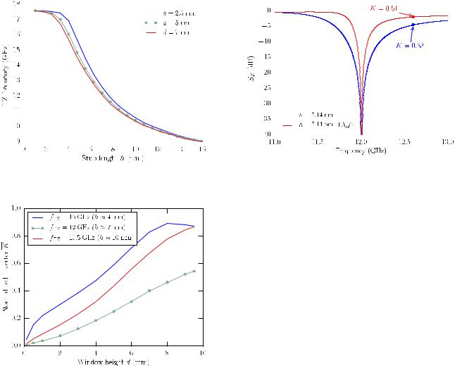
Fig. 2. TZ frequency as a function of the stub length h for different values of d. The stub thickness (ls ) and window length (lw ) are set to 2 mm.
Fig. 4. Two different stub solutions, separated by λg /2, are able to realize the same TZ but enable the implementation of different inverter values.
Fig. 3. Normalized impedance inverter parameter as a function of the window height d. Simulations are performed at 12.6 GHz. For each curve, the stub length h is slightly adjusted to keep the TZ at the same frequency.
(normally limited by manufacturing constraints) to avoid bulky stubs. Thus, the TZ location can be controlled by adjusting h.
Once length h yields a proper location of the TZ, the capacitive window height d is adjusted until the obstacle provides an adequate normalized inverter value K . It is obtained from full-wave EM simulations as:
|
= |
|
|
1 |
− |S11| |
|
(2) |
|
K |
||||||||
1 |
+ |S11| |
|||||||
|
|
|
||||||
The reason to adjust the TZ first, and then the inverter value, is that the stub dimensions have an important effect on the total coupling level. However, the effect of the window dimensions on the location of the TZ is much smaller. This is confirmed by EM simulations of one of these obstacles implemented in standard WR-75 waveguide. Fig. 2 reveals that the TZ can be located in a wide frequency range, and it is barely affected by a moderate change in the iris height d . In contrast, Fig. 3 represents the variation of the normalized impedance inverter parameter with the height of the capacitive window. For each curve, the stub length h is slightly adjusted to keep the TZ at exactly the same frequency. As expected,
the normalized inverter value can be controlled by adjusting the height of the capacitive window. However, for different TZ locations, the required window height differs.
After synthesizing the filter coupling windows, each resonator is simulated attached to its input/output windows (to consider the loading effect) and its length is adjusted to restore the desired resonant frequency. From this point, a final optimization of the complete structure can be carried out.
Note also that as a TZ approaches the filter passband (with the stub length h approaching an odd multiple of λg /4 at such frequency range), the maximum normalized inverter value that can be achieved decreases. In Fig. 3, the normalized inverter is computed at 12.6 GHz. As can be seen, the curve associated with a TZ at 12 GHz has much smaller values than the other two curves, associated with TZs that are farther from the simulation frequency. Certain moderate or wideband applications may require large coupling levels, while simultaneously ensuring that TZs are placed close to the passband. In these scenarios, we can benefit from the multiple solutions for the stub length that yield the same TZ location, according to (1). Take, for instance, the S21 parameter response of Fig. 4. One curve corresponds to the simulation of a stubiris structure with h = 7.14 mm, d = 6 mm, ls = lw = 2 mm. The other curve corresponds to the same structure except for the stub, which is λg /2 longer. The TZ associated with this longer stub has a much narrower bandwidth. This means that it can provide larger values of the S21 parameter for frequencies close to the TZ. Consequently, the S11 parameter is smaller near the TZ, and thus the normalized inverter K is larger. Effectively, by increasing the length of the stub by λg /2 we can implement larger coupling elements while still realizing TZs that are close to the passband. However, these solutions may generate unwanted resonances in the stopband. For that reason, they are only employed if shorter solutions are not able to yield an adequate inverter value.
Another interesting application of these obstacles is found in filters that contain very thin coupling windows, which may be difficult to manufacture. The introduction of a stub next to a capacitive window reduces the overall coupling provided by the obstacle. To compensate for the loss of coupling, the size of the capacitive window has to be increased. This is a positive consequence, since the window is now easier to manufacture, and more robust to potential manufacturing deviations.

This article has been accepted for inclusion in a future issue of this journal. Content is final as presented, with the exception of pagination.
CARCELLER et al.: CAPACITIVE OBSTACLE REALIZING MULTIPLE TRANSMISSION ZEROS FOR IN-LINE RECTANGULAR WAVEGUIDE FILTERS |
3 |
Fig. 5. a) Physical structure of the designed filter containing three stubs. b) Measurements from a manufactured prototype are successfully compared with EM simulations.
The main drawback of this obstacle is that it generates undesired resonances associated with the stub, limiting the spurious-free band. To shift these resonances away from the stopband, several solutions apply: readjusting the stub width ls , changing the wall (top or bottom) where the stubs are placed and/or reducing the height of the adjacent resonator.
III. RESULTS
The practical applicability of this coupling structure will be shown with a five-pole all-capacitive filter centered at 12.6 GHz and with 400 MHz bandwidth. This structure includes three stubs, realizing TZs on both sides of the passband.
The highest-frequency TZ is adjacent to the passband, separated 170 MHz from the edge. As was previously discussed and shown in Fig. 3, this fact limits the normalized inverter value that can be achieved by the stub-iris combination. In a Chebyshev filter, the irises that implement the smallest impedance inverters are the central ones. Consequently, the stub associated with this TZ is implemented there. The two TZs below the passband could be assigned to any other iris, since there seems to be no serious coupling limitation. In this case, they are both assigned to the other central iris (see Fig. 5a), demonstrating the capability of a single capacitive window to support multiple stubs.
An initial value for the normalized impedance inverters can be obtained from an all-pole distributed model [6]. From these values, the all-pole version of the filter is constructed.
Then, stubs are introduced in order to generate the TZs. This forces a readjustment of the corresponding coupling windows and adjacent resonator lengths before recovering the filter response in its passband. The resulting structure is shown in Fig. 5a. In contrast with all-pole filters, note that the central coupling windows (with stubs) are not the narrowest ones, thus improving the manufacturing sensitivity and the powerhandling capability of the filter.
A prototype has been manufactured in bare aluminum. Measurements are successfully compared, in Fig. 5b, with full-wave simulations provided by FEST3D. As can be seen, the location of the TZs is perfectly predicted by the EM simulations with a maximum deviation of 14 MHz. It is also clear that the presence of a TZ close to the upper edge of the passband makes the in-band response around this edge more sensitive to manufacturing deviations. However, this effect was expected after performing a tolerance analysis [7] on the filter, and can be compensated in practical applications with strict passband specifications and wider design margins. Finally, the peak observed at 10.8 GHz is a resonance generated by the combination of resonators 3 and 4 of the filter (see Fig. 5a), which are strongly coupled at low frequencies by the wide iris placed between them (that is required after placing the highest-frequency TZ very close to the passband).
IV. CONCLUSION
This paper proposes a new capacitive rectangular waveguide obstacle that enables the realization of TZs in a simple and direct way. This block is composed of one or two stubs attached to a classical capacitive window, thus enabling the realization of up to two TZs. This compact obstacle offers great flexibility to prescribe the location of the TZ in a wide frequency range, and can be employed to implement external and inter-resonator couplings. Practical guidelines for designing filters including this type of obstacle have been given. Likewise, a filter prototype has been designed and manufactured to illustrate the practical use of this obstacle.
REFERENCES
[1]R. M. Kurzrok, “General three-resonator filters in waveguide,” IEEE Trans. Microw. Theory Techn., vol. 14, no. 1, pp. 46–47, Jan. 1966.
[2]A. E. Atia and A. E. Williams, “Narrow-bandpass waveguide filters,”
IEEE Trans. Microw. Theory Techn., vol. 20, no. 4, pp. 258–265, Apr. 1972.
[3]S. Amari and G. Macchiarella, “Synthesis of inline filters with arbitrarily placed attenuation poles by using nonresonating nodes,” IEEE Trans. Microw. Theory Techn., vol. 53, no. 10, pp. 3075–3081, Oct. 2005.
[4]S. Amari and J. Bornemann, “Using frequency-dependent coupling to generate finite attenuation poles in direct-coupled resonator bandpass filters,” IEEE Microw. Guided Wave Lett., vol. 9, no. 10, pp. 404–406, Oct. 1999.
[5]N. Marcuvitz, Waveguide Handbook. New York, NY, USA: McGraw-Hill, 1951.
[6]G. L. Matthaei, E. M. T. Jones, and L. Young, Microwave Filters, Impendence-Matching Networks and Coupling Structures. New York, NY, USA: McGraw-Hill, 1964.
[7]P. Soto, V. E. Boria, C. Carceller, C. P. Vicente, J. Gil, and B. Gimeno, “EM-based synthesis and design of bandpass waveguide filters including manufacturing effects with FEST 3D,” Int. J. RF Microw. Comput.-Aided Eng., vol. 22, no. 1, pp. 93–103, 2012.