

диафрагмированные волноводные фильтры / d81b895b-a623-4ba2-ab54-dfde2b237b2d
.pdf106 |
IEEE TRANSACTIONS ON TERAHERTZ SCIENCE AND TECHNOLOGY, VOL. 9, NO. 1, JANUARY 2019 |
THz Letters
Micromachined Filters at 450 GHz With 1% Fractional Bandwidth and
Unloaded Q Beyond 700
Oleksandr Glubokov  , Xinghai Zhao, James Campion
  , Umer Shah
  , and Joachim Oberhammer
Abstract—This letter presents two silicon-micromachined narrowband fourth-order waveguide filter concepts with center frequency of 450 GHz, which are the first narrowband submillimeter-wave filters implemented in any technology with a fractional bandwidth as low as 1%. Both filters designs are highly compact and have axial port arrangements, so that they can be mounted directly between two standard waveguide flanges without needing any split-block interposers. The first filter concept contains two TM1 1 0 dual-mode cavities of circular shape with coupling slots and perturbations arranged in two vertically stacked layers, while the second filter concept is composed of four TE1 0 1 series resonators arranged in a folded, two-level topology without crosscouplings. Prototype devices are fabricated in a multilayer chip platform by high-precision, low-surface roughness deep-silicon etching on silicon-on-insulator wafers. The measured passband insertion loss of two prototype devices of the dual-mode circularcavity filters is 2.3 dB, and 2.6 dB for three prototypes of the folded filter design. The corresponding extracted unloaded quality factors of the resonators are 786 ± 7 and 703 ± 13, respectively, which are the best so far reported for submillimeter-wave filters in any technology. The presented filters are extremely compact in terms of size; their footprints have areas of only 0.53 and 0.55 mm2, respectively, and the thickness between the waveguide flanges is 0.9 mm.
Index Terms—All-pole filters, dual-mode filters, microfabrication, micromachining technology, waveguide filters.
I. INTRODUCTION
Silicon micromachining is a fabrication technology that allows us to produce three-dimensional (3-D) and high aspect ratio geometries with micrometer sized features and high aspect ratios, thus enabling novel approaches to design high-performance devices operating at millimeter and submillimeter-wave frequencies, in particular, when accurate geometries are needed as in the case of higher order filters. Micromachining facilitates parallel processing, i.e., many thousands of devices can be manufactured simultaneously on silicon wafers with high-product uniformity and high yield [1]. Recently, a novel micromachined
Manuscript received October 4, 2018; revised November 12, 2018; accepted November 12, 2018. Date of publication November 23, 2018; date of current version January 9, 2019. This work was supported in part by the European Research Council under the European Union’s Horizon 2020 Research and Innovation Programme under Grant 616846 and in part by the Swedish Foundation for Strategic Research Synergy Grant Electronics SE13-007. (Corresponding author: Oleksandr Glubokov.)
The authors are with the Department of Micro and Nanosystems, KTH Royal Institute of Technology, SE-100 44, Stockholm, Sweden (e-mail: glubokov@ kth.se; xinghai@kth.se; jcampion@kth.se; umers@kth.se; joachimo@kth.se).
Color versions of one or more of the figures in this letter are available online at http://ieeexplore.ieee.org.
Digital Object Identifier 10.1109/TTHZ.2018.2883075
waveguide technology has been reported, where a double H- plane split waveguide has shown only 0.02 dB/mm measured insertion loss (IL) at 330 GHz [2], and filters implemented in that technology showed outstanding results in the 110–170 [3] and in the 220–330 GHz bands [4].
At the moment, very few micromachined filter designs have been reported at frequencies above 300 GHz; a summary of the state of the art is shown in Table I. Most of prior-art filters are relatively broadband (fractional bandwidth, FBW, over 2%), for which the IL is naturally lower and good agreement between simulations and experiments is easier to achieve as compared to narrow-band filters.
In this letter, we present two different concepts of narrowband waveguide filters, designed for 450 GHz. The filters are implemented with axial port arrangement, which enables direct insertion of the filters between two standard WM-570 waveguide flanges without the need to fabricate additional metal blocks or sophisticated transitions. The filters shown in this letter achieve for the first time a FBW as low as 1%, and the so far highest measured unloaded Q factors ever reported in the literature for any submillimeter-wave filters in any technology, which also results in an outstanding low-IL.
II. FILTER DESIGN AND FABRICATION
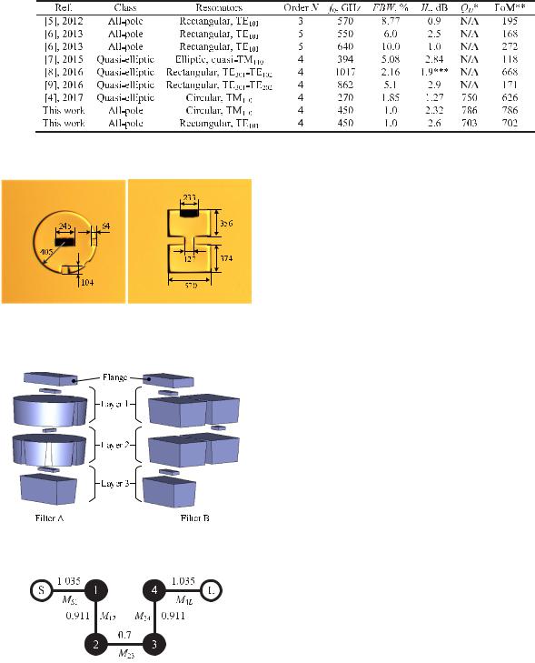
The first filter concept (referred to as concept A) is an all-pole filter with a pair of dual-mode circular cavities, each accommodating a pair of degenerate TM110 modes with vertically and horizontally polarized magnetic fields. This filter has a similar configuration as the dual-mode filter designed by our group at 270 GHz [4] but is implemented without the virtual negative crosscoupling between the cavities. The second filter concept (concept B) is a classical direct-coupled design [10], using TE101 rectangular waveguide cavities as the basic resonators but arranged in a folded manner in order to achieve axial port arrangement. Here, the first and the second resonators are situated in the same layer and coupled through a symmetric inductive iris. The second and the third resonators interact through a coupling slot located along the long sidewall of the resonators, thus establishing magnetic coupling. Input/output couplings are facilitated by means of horizontal slots between the feeding waveguides and the first and the fourth resonator, respectively. In Figs. 1 and 2, microscope pictures of fabricated prototypes and exploded views of the designed narrowband filter concepts are shown, respectively.
Both filter designs implement the same frequency response that satisfies the following design specifications:
1) center frequency: f0 = 450 GHz;
2156-342X © 2018 IEEE. Personal use is permitted, but republication/redistribution requires IEEE permission. See http://www.ieee.org/publications standards/publications/rights/index.html for more information.
IEEE TRANSACTIONS ON TERAHERTZ SCIENCE AND TECHNOLOGY, VOL. 9, NO. 1, JANUARY 2019 |
107 |
TABLE I
STATE-OF-THE-ART SILICON-MICROMACHINED FILTERS OPERATING AT FREQUENCIES ABOVE 260 GHZ AND RESULTS OF THIS WORK
Extracted from measured data.
Figure of merit for filter performance, calculated as 21.5·N·(f0 )1/2 /(IL·FBW).
Estimated losses.
Fig. 1. Microscope pictures of two fabricated prototypes of the two filter concepts. (a) Circular dual-mode TM1 1 0 cavity of filter concept A. (b) Two cavities of filter concept B, coupled through an inductive iris. All dimensions are in micrometer.
Fig. 2. Exploded views of the designed filter concepts A and B. Each layer represents a SOI wafer chip and consists of a handle layer (thick, with cavities) and device layer (thin, with slots).
Fig. 3. Coupling scheme of the filter design, implemented for both concepts A and B.
2)bandwidth: BW = 4.5 GHz (1% FBW); and
3)return loss in passband: RL = 20 dB.
The corresponding coupling scheme of the filters along with the coupling coefficients of the filter prototypes are displayed in Fig. 3. Design procedure for the filters is described as follows. At first, initial sizes of the cavities are determined by tuning their dimensions so as to match their resonant frequencies with
the center frequency of the filter using the eigenmode solver in CST Microwave Studio. Then, external couplings (MS 1 , M4L ) and couplings between the pairs of the resonators (M12 , M23 , M34 ) were examined through simulations and tuned in order to match the prototype values by changing dimensions of the corresponding irises, slots, and perturbations. All the coupling coefficients are extracted using a well-known procedure [11]. Eventually, the entire filter structures are simulated with the obtained dimensions, their coupling matrices are extracted through vector fitting algorithm [12] embedded in CST filter designer 3-D tool, and the responses of the filters are fine-tuned by matching the extracted coupling matrix entries with the prototype values.
The filters consist of three stacked silicon micromachined chips fabricated on silicon-on-insulator (SOI) wafers (handle layer and device layer thickness of 275 μm and 30 μm, respectively). The two top chips contain the cavities, the coupling perturbations or irises, and the input and internal coupling slots (layers 1 and 2, see Fig. 2); the bottom chip (layer 3) accommodates the output slots and the waveguide opening. The total size of the entire chip with five test filters (2 of concept A, 3 of concept B), including waveguide-flange alignment holes and other auxiliary elements, is 20 × 8 mm2. The footprint of a single filter of concept A is 0.53 mm2, and 0.55 mm2 for a filter of concept B. The dimensions of the filters are shown in Fig. 1.
The chips are fabricated in a two-mask micromachining process on SOI wafers, using silicon dioxide photolithography masks. The cavities and the couplings slots are fabricated by deep-reactive ion etching using a modified BOSCH-process in an Applied-Materials Centura tool. Using the tool, we can achieve fast switching of gases, which significantly improves surface roughness on the sidewalls. The etching process creates a slightly tilted but highly-reproducible sidewall profile, which was taken into account at the design phase by evaluating the sidewall profile of test fabrication runs. Each chip is metallized by sputtering a 1-μm thick layer of gold. The metallized chips are then assembled into a three layers stacked configuration and bonded using thermo-compression bonding, resulting in a 0.9-mm-thick device. The flange-to-microchip alignment accuracy is greatly enhanced by using a method with a pair of circular-elliptic flange alignment holes, which was recently published in [13].
III. EXPERIMENTAL VERIFICATION
For characterization, the filters were directly placed between standard WR-2.2 waveguide flanges and measured using a

108 |
IEEE TRANSACTIONS ON TERAHERTZ SCIENCE AND TECHNOLOGY, VOL. 9, NO. 1, JANUARY 2019 |
The measurements of all filter prototypes are characterized by a slightly detuned return loss due to minor assembly inaccuracies, but still being around or better than 20 dB for the major part of the passband. The filters show the best so far reported combination of fractional bandwidth and measured ILs in passband, as summarized in Table I.
In addition, we estimated the effective conductivity of the metallization for both types of filters, using the extracted Q- factor values, to σAu = 2.3 × 10⁷ S/m (approx. 50% of the ideal gold bulk resistivity value), which was applied to calculate the simulation responses in Figs. 4 and 5, which resulted in a very good agreement of the measured average IL in the passband.
IV. CONCLUSION
Fig. 4. Measured and simulated responses of two filter prototypes (A1, A2) filters of concept A.
Two narrowband waveguide filters with 4.5 GHz bandwidth operating at 450 GHz have been presented. The dual-mode filter with circular cavities has shown just 2.3 dB IL in passband, while the folded all-pole filter with TE101 resonators has displayed 2.6 dB. Quality factors of the resonators have been extracted from the measurement results. The presented designs are the first ever reported narrowband submillimeter-wave filters with fractional bandwidth as low as 1%, in any technology. In addition, the best ever measured Q factor in any technology has been reported for submillimeter-wave filters.
Fig. 5. Measured and simulated responses of three prototypes (B1, B2, B3) of concept B.
Rohde&Schwarz ZVA24 vector network analyzer with two WM-570 millimeter-wave converters by VDI for 325–500 GHz. Calibration was done at the waveguide flanges using a Thru- Reflect-Line standard.
Fig. 4 shows the responses of two filter prototypes of concept A, compared to the simulation data. Both filter prototypes have near identical results, i.e., the fabrication process is very uniform and well reproducible; however, they are shifted by approx. 2 GHz (0.44% of the f0 ) with respect to the simulated data. This happened due to slightly larger underetching than estimated in the test fabrication runs using slightly smaller cavities. The detuning of the measured return losses is explained by the influence of a small misalignment between adjacent layers of the chip stack. The IL in the passband is 2.3 dB. The unloaded quality factor of the dual-mode cavity resonators, extracted from the two measurements, is 786 ± 7 (1σ, 2 chips).
The measured responses of the filter prototypes of concept B are shown in Fig. 5, together with the simulated data. Similarly to the filters of concept A, the measured response of the prototypes is almost identical, but also exhibits a frequency shift by about 3 GHz (0.67% of the f0 ), as compared to the simulation data, due to the same effect. Also, a minor widening of the passband is observed, which could be traced to the window of the coupling iris being slightly enlarged. Since the relative shift of the passband is larger for filters of concept B, the dual-mode filters are less sensitive to the enlargement of the cavities during fabrication. The IL in passband for the filter prototypes of concepts B is 2.6 dB. The corresponding unloaded quality factor extracted from the measurements is 703 ± 13 (1σ, 3 chips).
REFERENCES
[1]M. Sterner et al., “Microwave MEMS devices designed for process robustness and operational reliability,” Int. J. Microw. Wireless Technol., vol. 3, no. 5, pp. 547–563, 2011, doi: 10.1017/S1759078711000845.
[2]B. Beuerle, J. Campion, U. Shah, and J. Oberhammer, “A very low loss 220–325 GHz silicon micromachined waveguide technology,” IEEE Trans. THz Sci. Technol., vol. 8, no. 2, pp. 248–250, Mar. 2018, doi: 10.1109/TTHZ.2018.2791841.
[3]J. Campion et al., “An ultra low-loss silicon-micromachined waveguide filter for D-band telecommunication applications,” in Proc. IEEE MTT- S Int. Microw. Symp., Philadelphia, PA, USA, 2018, pp. 583–586, doi: 10.1109/MWSYM.2018.8439601.
[4]O. Glubokov et al., “Micromachined multilayer bandpass filter at 270 GHz using dual-mode circular cavities,” in Proc. IEEE MTT-S Int. Microw. Symp., 2017, pp. 1449–1452, doi: 10.1109/MWSYM.2017.8058894.
[5]K. M. K. H. Leong et al., “WR1.5 silicon micromachined waveguide components and active circuit integration methodology,” IEEE Trans. Microw. Theory Techn., vol. 60, no. 4, pp. 998–1005, Apr. 2012, doi: 10.1109/TMTT.2012.2184296.
[6]C. A. Leal-Sevillano et al., “Silicon micromachined canonical E-plane and H-plane bandpass filters at the terahertz band,” IEEE Microw. Wireless Compon. Lett., vol. 23, no. 6, pp. 288–290, Jun. 2013, doi: 10.1109/LMWC.2013.2258097.
[7]J. X. Zhuang, Z. C. Hao, and W. Hong, “Silicon micromachined terahertz bandpass filter with elliptic cavities,” IEEE Trans. THz Sci. Technol., vol. 5, no. 6, pp. 1040–1047, Nov. 2015, doi: 10.1109/TTHZ.2015.2480844.
[8]S. Liu et al., “1 THz micromachined waveguide band-pass filter,” J. Infrared, Millimeter, THz Waves, vol. 37, no. 5, pp. 435–447, 2016, doi: 10.1007/s10762-015-0229-6.
[9]S. Liu et al., “Micromachined WR-1.0 waveguide band-pass filter,” in
Proc. IEEE Int. Conf. Microw. Millimeter Wave Technol., Jun. 2016, vol. 2, pp. 949–951, doi: 10.1109/ICMMT.2016.7762496.
[10]R. J. Cameron, C. M. Kudsia, and R. R. Mansour, Microwave Filters for Communication Systems: Fundamentals, Design, and Applications. Hoboken, NJ, USA: Wiley, 2007, doi: 10.1002/9781119292371.
[11]J.-S. Hong and M. J. Lancaster, Microstrip Filters for RF/Microwave Applications. New York, NY, USA: Wiley, 2001, doi: 10.1002/0471221619.
[12]B. Gustavsen and A. Semlyen, “Rational approximation of frequency domain responses by vector fitting,” IEEE Trans. Power Del., vol. 14, no. 3, pp. 1052–1061, Jul. 1999, doi: 10.1109/61.772353.
[13]J. Campion, U. Shah, and J. Oberhammer, “Elliptical alignment holes enabling accurate direct assembly of micro-chips to standard waveguide flanges at sub-THz frequencies,” in Proc. IEEE MTT-S Int. Microw. Symp., 2017, pp. 1262–1265, doi: 10.1109/MWSYM.2017.8058838.