

диафрагмированные волноводные фильтры / c1709068-1fb8-412f-b4d9-8c2a25f3bd81
.pdfMicromachined J-band Rectangular Waveguide Filter
M. Vahidpour, K.Sarabandi
Radiation Laboratory, Department of Electrical Engineering and Computer Science, University of Michigan Ann Arbor, Michigan, 48109, {mvahid, saraband}@umich.edu
Abstract
Fully micromachined waveguide filters are realized based on metal E-plane rods. The rods make a series of shunt inductors separated by the length of the waveguide. Twoand threepole filter designs for 230~245 GHz bands constructed in WR-3 waveguide are introduced. The filters are microfabricated by etching the rods and waveguides on one silicon wafer which later is bonded with another metal-coated wafer. The devices are measured using a J-band S- parameter test and the measurement results are in good agreement with the simulation results.
1. Introduction
In the past decade, high millimeterand submillimeter-wave frequencies have found widespread applications in communications, navigation, radiometry, active and passive imaging, detection of concealed explosives, etc. Meanwhile, the need to employ compact and low-cost fully integrated circuits on a single chip has become more noticeable. The emphasis of recent systems operating at the atmospheric window above 200 GHz is on the advances of the active components on low-noise high electron mobility transistors (HEMTs). Fully integrated MMIC receiver and transmitter based on CMOS, InP, SiGe and GaAs on coplanar waveguides (CPW) have recently been developed ([1]-[6] in [1]). The implementation on CPW lines provides compact planar geometry and ease of integration of shunt and series elements. In addition, the design of microwave probes for on-wafer characterization of millimeter-wave integrated circuits is another important motivation to employ CPW lines. However, in all planar transmission lines, loss increases as frequency is increased. On the other hand, hollow rectangular waveguides are widely used at higher frequencies as antenna feeds and filters due to their superior low loss characteristics, and high power handling capabilities. Because of these features, it is common to fabricate passive components in rectangular waveguide medium at submillimeterand high millimeter-wave frequencies.
Waveguide filters, like ordinary filters are designed using reactive elements. These reactive components are usually realized by inserting discontinuities or obstacles such as rods or diaphragms along the length of the host waveguide. At microwave and low millimeter wave frequencies, these filters are fabricated by cutting slits in the crosssection of the waveguide, inserting the element inside and finally soldering the edges. However, standard machining methods are not suitable for high MMW applications because of low fabrication tolerances and high cost in assembly. With the advances on silicon micromachining, this approach has been used to fabricate rectangular waveguide and high- Q cavity structures from Ka- [2] to W-band [3]. Most of the early work in micromachining involved creating the waveguide height by stacking layers of etched silicon wafers. However, this technique needs high-quality wafer-to- wafer metallic bonds in order to prevent interruption of the current flow [4]. There have been several attempts to fabricate W-band waveguides with lithography. However, in these techniques, the height of the waveguide is limited by the maximum thickness of the spun photoresist, limiting the fabrication to the reduced-height waveguides which suffer from high attenuation. Taking advantage of the "snap-together" technique, a rectangular waveguide was fabricated in two halves and then the halves were put together to form a complete waveguide [3]. An alternate technique to etch the waveguide is deep reactive ion etching (DRIE) of silicon which is a viable approach for fabrication of high-performance micromachined waveguide structures. In [5] both diamond and rectangular waveguide were fabricated by bonding two halves of the waveguide. A waveguide based two-pole filter using iris was realized by stacked layers of silicon wafers in [6]. These methods involve a high degree of fabrication complexity, complex three-dimensional geometries and assemblies of various parts. Also, high quality assemblies of different metallic parts are not achievable by only snapping the parts together especially at high MMW frequencies where superior metal-to-metal contact is essential.
In this study, we propose a micromachined E-plane fully-metallic rectangular waveguide filter for J-band (220~ 325 GHz) applications. In this structure, the required susceptance for filter is obtained by metal rods in the E-plane which extend all the way across the cross section of the waveguide, separated by the lengths of the waveguide as the impedance transformers. The filter is fabricated on two silicon wafers which are later gold-coated and bonded using high quality gold thermocompression bonding.
978-1-4244-6051-9/11/$26.00 ©2011 IEEE
2. Filter Design
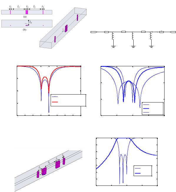
In E-plane pure metal insert filters the insert connects the broad walls of a rectangular waveguide. The proposed filter topology is shown in Fig. 1. Depending on the number of poles, it consists of a number of rods serving as inductances separated by lengths of the waveguide. This structure is simpler than iris, since the inserts are rod shape and do not deform along the cross-section of waveguide. Therefore, they can be easily fabricated using single-step etching of silicon. The standard WR-3 waveguide (a = 864 µm, b = 432 µm) along with rods with h = 432 µm and cross sections larger than 50 µm × 50 µm – to provide mechanical rigidity - are assigned to design filters with various passbands at J-band. This filter can be modeled by an equivalent circuit model shown Fig. 1 (c). It is well-known that a rod terminated by the broad wall of a rectangular waveguide acts as an inductive element whose inductance is inversely proportional to its cross-section size and the waveguide dimensions [7]. By changing the dimensions the cross-sections of the rods the desired inductance values can be designed. The spacing between the rods is an impedance transformer whose length is a quarter of a guiding wavelength of the fundamental TE10 mode of the waveguide. Fig. 2 (a) shows the response (full-wave analysis with Ansoft HFSS) of the two-pole filter (with three rods) shown in Fig. 1 compared to the response of the circuit model. It is designed to have the pass band at 230~245 GHz and the nulls around 235 and 240 GHz. In this structure, the length of the impedance transformer is considered (2+1/4) λ in order to limit the bandwidth to 230~245 GHz. For wider band applications, the length could be decreased to (1+1/4) λ or λ /4 as shown in Fig. 2 (b).
Another filter with three-pole (four rods and three connecting lines) is also designed for the same frequency band. The total length of this filter is shorter since the spacing is kept at λ /4 and the roll-off is higher since one more pole is added. The response of the filter is shown in Fig. 3. Higher order filters can also be realized with this method depending on the application.
3. Fabrication and Measurement
In order to excite the structure with GSG probes, the in-plane CPW to waveguide transition introduced in [8] is used. The transition is used at both ends of the waveguide in order to be able to measure the S-parameters of the back- to-back structure.
The waveguide filters presented here are fabricated using the method described in [8]. Since the rods have the same height as the waveguide and they do not deform along the cross-section, they can be fabricated with the same procedure as waveguide by etching a single substrate. The microfabrication procedure is based on etching the waveguide height and rods on one silicon wafer, gold deposit the surface to make the structure conductive and bonding another gold-deposited silicon wafer to form the waveguide structure as shown in Fig. 4 (a). The waveguide trench is etched with DRIE method to achieve vertical sidewalls. The structure is then gold-sputtered so that the sidewalls are also covered with gold as well as top and bottom to form a fully conductive filter. Finally, the wafers are aligned in contact and high quality gold-gold thermocompression bonding is applied to form a sealed waveguide. For measurement purposes, additional steps of multi-step silicon etching and fabricating CPW to waveguide transition is required which are explained in [8] in detail. Fig. 4 (b) shows the fabricated bottom wafer of the two-pole filter of Fig. 1 before gold-gold bonding to the top wafer. Fig. 5 shows the three-dimensional interferometric image of the rods after gold deposition. The fabrication processes have been carried out at the University of Michigan Lurie Nanofabrication Facilities.
S-parameter measurement of the filter is performed using dual source PNA-X with OML frequency extenders shown in Fig. 6. The structure is fed through GSG probes connected to the frequency extending modules using WR-3 bent waveguides controlled by Cascade Microtech MMW micropositioners. On-substrate TRL calibration lines are measured first to de-embed the effect of the CPW line. In addition, the response of a back-to-back transition is also deembedded from the final response of the filter. After calibration, S-parameters of the filter is measured and presented in Fig. 7. The measurement results show a good agreement with the simulation. The deviation can be attributed to error in the precision of the etch depth and the quality of the boding of the rods to the top wafer.
7.References
1.M. Abbasi, et.al ,”Single-Chip 220-GHz Active Heterodyne Receiver and Transmitter MMICs With On-Chip Integrated Antenna”, IEEE. Trans. Microwave Theory Tech., pp. 466-478, Feb. 2011.
2.M. T. Stickel, P. C. Kremer, and G. V. Eleftheriades, “High-Q silicon micromachined cavity resonators at 30 GHz using the split-block echnique,” Proc. Inst. Elect. Eng., vol. 151, no. 5, pp. 450–454, Oct. 20, 2004.
3.C. E. Collins, et. al. “A new micro-machined millimeter-wave and terahertz snaptogether rectangular waveguide technology,” IEEE Microw. Guided Wave Lett., vol. 9, pp. 63–65, Feb. 1999.
4.M. Stickel, “A millimeter-wave bandpass waveguide Filter Using a Width-Stacked Silicon Bulk Micromachining Approach, “IEEE Microwave Wireless Comp. Lett, pp. 209-211., Apr. 2006
5.Y. Lee, J. P. Becker, J. East, L. P. B. Katehi, “Fully micromachined finite-ground coplanar line-to-waveguide transitions for w-band applications,”
IEEE Trans. Microwave Theory Tech., vol. 52, pp. 1001-1007, Mar. 2004
6.Y. Li, B. Pan, C. Lugo, M. M. Tentzeris, and J. Papapolymerou, "Design and characterization of a W-band micromachined cavity filter including a novel integrated transition from CPW feeding lines," IEEE Trans. Microwave Theory Tech., vol. 55, pp. 2902-2910, Dec. 2007
7.R. F. Harrington, Time-Harmonic Electromagnetic Fields, McGraw-Hill, New York, 1961, pp. 177-179 and 425-428.
8.M. Vahidpour, K. Sarabandi, “In-plane cavity-backed coplanar waveguide to rectangular waveguide transition for micromachining applications,” submitted to IEEE Trans. Microwave Theory Tech.
(c)
Fig. 1. The structure of E-plane two-pole filter (a) side view (b) top view. (c) The equivalent circuit model.
|
0 |
|
0 |
|
-20 |
|
|
|
|
|
-20 |
) |
|
|
) |
11 |
-40 |
|
11 |
dB(S |
|
dB(S |
|
|
Circuit Model |
||
|
|
|
|
|
|
|
|
Full-wave Simulation |
-40 |
|
|
|
|
|||
-60 |
|
|
|
|
|
|
|
|
|
||||
|
|
|
|
(HFSS) |
|
|
|
|
|
l=λ/4+λ |
|
||
|
|
|
|
|
|
|
|
|
|
|
|||
|
|
|
|
|
|
|
|
|
|
|
|
|
|
|
|
|
|
|
|
|
|
|
|
|
|
l=λ/4+λ /2 |
|
|
|
|
|
|
|
|
|
|
|
|
|
l=λ/4 |
|
-80 |
225 |
230 |
235 |
240 |
245 |
250 |
255 |
260 |
-60 |
230 |
240 |
250 |
260 |
220 |
220 |
||||||||||||
|
|
|
Frequency (GHz) |
|
|
|
|
|
Frequency (GHz) |
|
|
||
|
|
|
(a) |
|
|
|
|
|
|
|
(b) |
|
|
Fig. 2. (a) The reflection coefficient of the filter presented in Fig. 1 with t1=75 µm, l1=2.344 mm, t2=365 µm, l2= l1, t3= t1, l3= 638.6 µm. (b) The response of the same filter with various values for l= l2= l1 maintaining λ /4 difference.
0 |
|
|
|
|
-10 |
|
|
|
|
-20 |
|
|
|
|
-30 |
|
|
|
|
dB |
|
|
|
|
-40 |
|
|
|
|
|
|
|
dB(S11) |
|
-50 |
|
|
dB(S21) |
|
|
|
|
|
|
-60 |
|
|
|
|
-70 |
230 |
240 |
250 |
260 |
220 |
||||
|
|
Frequency (GHz) |
|
|
(a) (b)
Fig. 3. (a) The structure of the three-pole filter. (b) The response of the filter for with t1=117 µm, l1= 636 µm, t2=466 µm, l2=1.562 mm, t3= t1, t4= t2, l3= l1, l4= l2

|
Top wafer |
|
|
Bonding |
rods |
gold-coating |
|
|
Bottom wafer |
|
|
|
|
CPW-Waveguide transition |
rods |
|
(a) |
|
(b) |
Fig. 4. (a) Microfabrication process of the E-plane waveguide filter. (b) The fabricated structure before bonding. The CPW to waveguide transition in [8] used to excite the waveguide with GSG-probes
Fig. 5. three-dimensional interferometric image of the rods after gold deposition
Fig. 6. MMW S-parameter measurement setup.
|
0 |
|
|
|
|
|
0 |
|
|
|
|
|
-5 |
|
|
|
|
|
|
|
|
|
|
|
|
|
|
|
|
|
-5 |
|
|
|
|
|
-15 |
|
|
|
|
|
|
|
|
|
|
) |
|
|
|
|
|
) |
|
|
|
|
|
11 |
|
|
|
|
|
21 |
-10 |
|
|
|
|
dB(S |
-25 |
|
|
|
|
dB(S |
|
|
|
|
|
|
|
|
|
|
|
|
Measurement |
|
|||
|
|
|
|
Measurement |
|
|
|
|
|
Simulation |
|
|
|
|
|
|
|
|
|
|
|
|
|
|
-35 |
|
|
Simulation |
|
|
-15 |
|
|
|
|
|
|
|
|
|
|
|
|
|
|
|
|
|
-45 |
230 |
240 |
250 |
260 |
|
-20 |
230 |
240 |
250 |
260 |
|
220 |
|
220 |
||||||||
|
|
|
Frequency (GHz) |
|
|
|
|
|
Frequency (GHz) |
|
|
|
|
|
(a) |
|
|
|
|
|
(b) |
|
|
Fig. 7. Measured (a) reflection and (b) transmission coefficient of the filter shown in Fig. 1 compared to the full-wave simulation. The nulls of the |
|||||||||||
filter are precisely detected and the results are in good agreement with the simulation. |
|
|
|
||||||||