

диафрагмированные волноводные фильтры / b1f08cce-e6b4-487a-8c92-40b493ec56eb
.pdf816 |
IEEE TRANSACTIONS ON COMPONENTS AND PACKAGING TECHNOLOGIES, VOL. 32, NO. 4, DECEMBER 2009 |
Coplanar Waveguide Filters Based on Multibehavior Etched-Ground Stubs
Marwa Abdel Aziz, Member, IEEE, Amr M. E. Safwat, Member, IEEE, Florence Podevin,
and Anne Vilcot
Abstract—In this paper, coplanar waveguide filters with etched-ground stubs that have multiple behaviors are proposed. The response of a unit cell is a bandreject with one or more transmission zeros according to the number and the lengths of the stubs. A library of transmission line models is being built for the basic cells and then used for the design of more elaborated structures. The potential of these new topologies is highlighted by providing different filtering structures with interesting features: a second-order narrow bandpass filter, and two configurations for a lowpass filter with a wide stopband. All theoretical predictions have been verified by electromagnetic simulation and measurements.
Index Terms—Coplanar waveguide, coupled resonators, defected ground structures, filters, transmission lines.
I. Introduction
THE RAPID growth of telecommunications systems (worldwide interoperability for microwave access, wire-
less local area networks, satellite, wireless fidelity, etc.) has exponentially increased the number of users. However, the frequency spectrum is still a limited resource. The requirements imposed on the filtering stages are consequently becoming harder to achieve using the topologies adopted since the 1990s. This fact has urged the researchers to investigate new filtering structures that are simple, easy to design and implement, and characterized by a high-isolation and low-insertion loss.
Slotted “defected” ground structures were initially presented in [1] as a subcategory of the electromagnetic bandgap (EBG) structures. The goal was to locally change the guided wave properties by etching a lattice shape in the ground plane of a microstrip line, thus providing a filtering effect. The defected ground structures showed microwave properties similar to those of the EBG structures. Moreover, they turned to be much easier to model and to manufacture. They have then shown a huge evolution in terms of the defect shape. This
Manuscript received March 31, 2008; revised March 12, 2009. Current version published November 20, 2009. Recommended for publication by Associate Editor L. Li upon evaluation of reviewers’ comments.
M. Abdel Aziz, F. Podevin, and A. Vilcot are with the Institut de Microélectronique, Electromagnétisme et Photonique, Grenoble 38016, France (e-mail: marwa.mohamed@ieee.org; podevin@minatec.inpg.fr; vilcot@minatec.inpg.fr).
A. M. E. Safwat is with the Department of Electronics and Communications Engineering, Ain Shams University, Cairo 11517, Egypt (e-mail: asafwat@ieee.org).
Color versions of one or more of the figures in this paper are available online at http://ieeexplore.ieee.org.
Digital Object Identifier 10.1109/TCAPT.2009.2030418
work essentially lies on dumbbell-shaped structures [2] and its modifications as well as L-shaped lattices [3]. Coplanar filters based on the etching of a rectangular slot in the ground plane of a coplanar waveguide line have already been introduced as the conventional dumbbell structures in [2]. A modification has been presented in [4] with the insertion of a patch in the etched-rectangular area. Then, short circuits have been added between the patch and the ground plane. However, the modified dumbbell structures together with their equivalent circuits in [4] lacked the physical interpretation of the theory of operation. In this paper, a library of models for possible configurations of the modified dumbbell filter is built. These models are then considered as the basic building blocks in more elaborated filtering structures. The proposed design technique has the advantage of saving the huge simulation time consumed by the 3-D electromagnetic (EM) simulators in solving closely coupled resonant structures. The proposed model has been verified and compared to the EM solver and the previous transmission line results for the secondorder narrow bandpass filter of [5]. The paper then presents two different topologies for a lowpass filter with a wide stopband where the design procedure is based on the proposed transmission line model.
The paper is organized as follows. Section II presents the proposed modeling procedure and the corresponding results for the basic configurations. Section III presents the applications. The paper ends with the conclusion in Section IV.
II. Modeling of Coplanar Filters with Etched-Ground Stubs
A. Proposed Modeling Procedure
Figs. 1–3 show different configurations of the unit cell. They consist of a 6 mm × 6 mm square hole, etched in the ground plane of a 50 coplanar waveguide line, a square metallic patch, 5 mm × 5 mm centered inside the square hole, and short circuits that connect between the patch and the ground plane of the coplanar waveguide. The resulting slot behaves as an etched stub in the ground plane. Therefore, the corresponding response consists of a certain number of transmission zeros equal to the number of λ/2 and/or λ/4 etched stubs.
Fig. 1(a) presents the modified dumbbell where the etched stub resonates at one-half wavelength measured as the mean circumference around the patch. If we examine the orientation of the electric field along the slots of the etched stub presented
1521-3331/$26.00 c 2009 IEEE

ABDEL AZIZ et al.: COPLANAR WAVEGUIDE FILTERS BASED ON MULTIBEHAVIOR ETCHED-GROUND STUBS |
817 |
Fig. 2. Modified dumbbell filter with 2-D symmetry with four short circuits. Fig. 1. Modified dumbbell filter. (a) Schematic. (b) Equivalent circuit model. (a) Schematic. (b) Equivalent circuit model.
by the black arrows in Fig. 1(a), we would conclude that the horizontal slotlines outlined by the solid frame show an even mode distribution, while the vertical slotlines outlined by the dotted frame show an odd mode distribution as illustrated in the figure. Fig. 1(b) shows the equivalent circuit model where the resonator is partitioned into small sections of slotlines whose parameters are dependent on the orientation of the electric field in the original schematic. Fig. 4 summarizes the propagation parameters for each building block. In our case, the horizontal slotines are substituted by the model in Fig. 4(d) where the nearest slotine to the coplanar waveguide (CPW) main line is termed as Znear and the other slotine is termed as Zrear as illustrated in Fig. 1(b). The vertical slotlines are equivalent to the model in Fig. 4(f). The neck and the slotline T-junction are substituted by their equivalent models in Fig. 4(a) and (b), respectively.
Fig. 2(a) presents the schematic of the modified dumbbell filter when two short circuits are added to each resonator so as to maintain both the horizontal and the vertical symmetry. The resulting etched stub consists then of two series connected λ/4 stubs, which results in a bandreject filter with two equal transmission zeros. The near horizontal slotlines are almost uncoupled to the rear horizontal ones as outlined by the dashed frame in Fig. 2(a). These horizontal slotlines would be then replaced by the equivalent model of Fig. 4(c), which corresponds to an asymmetric slotline. While the vertical slotlines are still coupled and show an odd mode distribution as outlined by the dotted frame in Fig. 2(a). They would be replaced then in the equivalent circuit model by the transmission line section in Fig. 4(f). The short circuits are replaced by the equivalent inductance of Fig. 4(i). The resulting equivalent circuit is shown in Fig. 2(b).
Fig. 3(a) shows the dumbbell filter with horizontal symmetry only due to the addition of one short circuit per resonator. The etched stubs in Fig. 3(b) consist of two unequal λ/4 stubs connected in series whose response corresponds to a bandreject filter with two distinct transmission zeros. In this case, the horizontal slotlines outlined by the solid frame to the right
Fig. 3. Modified dumbbell filter with 1-D horizontal symmetry with two short circuits. (a) Schematic. (b) Equivalent circuit model.
in Fig. 3(a) show an even mode distribution, therefore they are modeled as in Fig. 4(d). While the horizontal slotlines in the region outlined by the double solid frame in Fig. 3(a) show an odd mode distribution and are consequently modeled as in Fig. 4(e). On the other hand, as shown in Fig. 3(a), the vertical slotlines show an odd mode distribution in the region outlined by the dotted frame and an even mode distribution in the region outlined by the dash-dot frame. They correspond then to the models shown in Fig. 4(f) and (g), respectively. The region of the vertical slotline which faces the short circuit is modeled as an asymmetric slotline following the parameters in Fig. 4(h).
According to the previous discussion, the etched stubs in the ground plane of the coplanar waveguide line are sectioned into simpler building blocks whose parameters are directly related to the dimensions and are easy to compute. These building

818 |
IEEE TRANSACTIONS ON COMPONENTS AND PACKAGING TECHNOLOGIES, VOL. 32, NO. 4, DECEMBER 2009 |
blocks are presented hereafter where the modeling parameters are specific to the FR4 substrate under study, characterized by 4.7 dielectric constant, 1.6 mm height and 0.016 loss tangent at 1 GHz. The substrate occupies a total area of 20 mm width and 30 mm length for all the basic cells presented within this paper. With reference to Fig. 1(a), these dimensions are maintained constant for any considered basic cells unless the contrary is stated, the gap width (g) is 1 mm, s1 = 1 mm, s2 = 5.5 mm, s3 = 7 mm, and d = 5 mm. The library of building blocks is presented hereafter.
1) The Neck: |
The neck is a 1 mm length slotline with |
0.5 mm gap width |
and 9.75 mm strip width on each side. |
Using CST Microwave Studio [6], the corresponding characteristic impedance is computed at 5 GHz as 82 and the effective dielectric constant is found to be 2.26. The neck is modeled, as shown in Fig. 4(a), as a four terminals lossless transmission line section.
2) The T-Junction: The slotline T-junction can be viewed as a planar E-plane T-junction where the input power from the neck is equally distributed between the horizontal arms with 180° phase shift. The T-junction is modeled, as shown in Fig. 4(b), as a center-tapped transformer, whose turn ratio is reduced from the theoretical value of 2:1 to 1.8:1. The insertion loss from the neck to each horizontal arm is theoretically −6 dB yet it was computed using [6] as −5 dB at 5.5 GHz. The 1 dB loss is attributed to the mismatch loss between the neck and each near horizontal arm.
3) Uncoupled Horizontal Slotlines: When the horizontal slotlines are not coupled to the rear ones as in the case shown in Fig. 2, each horizontal slotline is modeled as an asymmetric slotline of 0.5 mm gap width, 1 mm strip width on one side and 11 mm strip width on the other side corresponding to (d +g+s2). The corresponding characteristic impedance and the effective dielectric constant have been computed at 5 GHz by [6] as 103 and 2.56, respectively. The uncoupled horizontal slotline is modeled as shown in Fig. 4(c) as a lossless four terminals transmission line section of 2.25 mm length.
4) Adjacently Coupled Slotlines: As previously discussed, the electric field distribution along the slots between the patch and the ground plane in the structures shown in Figs. 1–3 implies a coupling between the adjacent slotlines. Therefore, the characteristic impedance of each slotline section is determined by either the even mode or the odd mode propagation parameters.
a) Coupling between horizontal slotlines: The slotline characteristic impedance and the effective dielectric constant have been computed using [7]. The voltage and current along each metal strip are provided by [7] as it is based on the method of moments. The three coupled strips for the horizontal slotlines are outlined by the solid frame in Fig. 1(a), the strip widths (s1, d, s2) are not identical. Therefore, there will be a discrepancy between the near and the rear slotlines characteristic impedances. According to the authors knowledge, [7] does not include the effect of dispersion, which is one possible source of error in the proposed model.
The transmission line models for the horizontal near and rear slotline sections are shown in Fig. 4(d) for an even mode distribution and in Fig. 4(e) for an odd mode distribution.
Fig. 4. Transmission line models for the building blocks of the proposed etched-ground filters, where Zc is the characteristic impedance of the slotline section, εeff is the effective dielectric constant of the slotline section, L is the
length of the slotline section, L’ is the inductance, Zeven is the even mode characteristic impedance, even is the even mode effective dielectric constant,
is the odd mode characteristic impedance, and odd is the odd mode effective dielectric constant. (a) Neck. (b) Slotline T-junction. (c) Uncoupled horizontal slotline. (d) Adjacently coupled horizontal slotlines (even mode).
(e) Adjacently coupled horizontal slotlines (odd mode). (f) Vertical slotline (odd mode). (g) Vertical slotline (even mode). (h) Vertical slotline facing a short circuit. (i) Terminating short circuit. (j) Short circuit with a coupled parasitic loop. (k) Coupling region between two cells closely separated by
0.95mm.
b)Coupling between vertical slotlines: The coupled vertical slotlines consist of three metal strips as shown by the dotted frame in Fig. 1(a). Due to the symmetry between left and right strip widths, there is no difference between the characteristic impedances of the right and the left slotlines. The corresponding model characteristics are computed using the 3-D EM solver [6] and are shown for the odd mode and the even mode in Fig. 4(f) and (g), respectively. The length of the vertical slotline depends on the position of the short circuit. Wherever, the vertical slotline is adjacent to a short circuit as in Fig. 3(a) the vertical slotline is then modeled as a slotline of 1 mm length with 0.5 mm gap width corresponding to a characteristic impedance of 82 and an effective dielectric constant of 2.26 as shown in Fig. 4(h).
5)Short Circuits: The characterization of short circuited slotlines has been studied by many authors, either experimentally [9] or analytically [10]. The short circuits are usually replaced by equivalent inductances. The inserted short

ABDEL AZIZ et al.: COPLANAR WAVEGUIDE FILTERS BASED ON MULTIBEHAVIOR ETCHED-GROUND STUBS |
819 |
circuits in all the proposed structures have 0.5 mm width and 1 mm length. The equivalent inductance is computed for a two-ports slotline with a strip width equal to the patch width (b) from one side and a strip width equal to the distance (s3) from the other side. A short circuit of 0.5 mm length is inserted midway between the two ports. The inductance has been calculated using the 3-D EM solver [6] by deembedding the input ports at the center plane of the short circuit. The ABCD matrix is then extracted and equated to that of a shunt impedance. The equivalent inductance is in the order of 0.3 nH as shown in Fig. 4(i). The short circuit ends the propagation of the electric field along the slot in all configurations except when the short circuits are misaligned and the vertical symmetry is violated. Therefore, the short circuit is then modeled as an inductance of 0.3 nH in parallel with a 1:1 transformer and a resistance of 1 k as shown in Fig. 4(j).
6) The Coupling Region Between Two Cells: The coupling region between any two cells is modeled as three coupled strips where the middle strip width is the separation distance between the two cells taken as 0.95 mm and the two outer strips widths are equal to the patch width, d. This region is modeled by the equivalent even and odd mode propagation parameters of three coupled coplanar strips. The four terminals coupled transmission lines are extended to eight terminals by the use of 1:1 transformers as shown in Fig. 4(k). This model requires no short circuits being inserted in the coupling region between the two cells.
B. Results
A library of transmission line models for the proposed basic cells is proposed for the different topologies of the coplanar waveguide filters with etched-ground stubs using the building blocks of Fig. 4(a–k). EM simulations and measurements are shown hereafter in order to confirm the performance predicted by the model for each case.
1) The Modified Dumbbell Filter: The modified dumbbell filter presented in Fig. 1(a) corresponds to a transmission line model consisting of two identical 50 coplanar waveguide section connected in series with the neck of Fig. 4(a), then to the T-junction of Fig. 4(b) followed by the slotline sections of Fig. 4(d) and (f). The vertical slotlines have a length of 5 mm. A schematic for the equivalent circuit model is shown in Fig. 1(b). Fig. 5 presents the S21 response for the modified dumbbell from measurements, EM simulation and the transmission line model. A very good agreement is observed for the frequencies below the resonance frequency while discrepancies arise afterwards. The shift introduced by the transmission line model can be accounted for by adding a shunt capacitance of about 1 pF in parallel to the neck. This would compensate for the added capacitance at frequencies above the resonance frequency [11].
2) 2-D Symmetry With Four Short Circuits: For the modified dumbbell with 2-D symmetry shown in Fig. 2(a), four short circuits are symmetrically placed with respect to the vertical slots so as to connect the patch to the coplanar waveguide ground plane. The schematic of the equivalent circuit model is shown in Fig. 2(b). The horizontal slotlines are
Fig. 5. Modified dumbbell of Fig. 1(a). (a) Experimental (solid line), transmission line model (gray line), and EM simulation (dashed line) S21 response.
(b) Schematic.
Fig. 6. 2-D symmetry modified dumbbell with four short circuits of Fig. 1(b). (a) Experimental (solid line), transmission line model (gray line), and EM simulation (dashed line) S21 response. (b) Schematic.
uncoupled to the parasitic loop and are consequently modeled as in Fig. 4(c), whereas each vertical slotline is modeled as in Fig. 4(f). The length of each vertical slotline is 2 mm. The symmetrically added short circuits prohibit the propagation of the electric field around the parasitic loop. Therefore, the short circuits are modeled as in Fig. 4(j).
Fig. 6 presents the S21 response where very good agreement is seen between the measurements, the EM simulation and the transmission line model. This is thanks to the additional short circuits which have reduced the equivalent capacitance of the etched resonator above the resonance frequency.
3)1-D Horizontal Symmetry With Two Short Circuits: The 1-D symmetry modified dumbbell in Fig. 3(a) behaves as the dual behavioral resonator proposed in microstrip technology in [12]. The longer λ/4 etched stub provides a transmission zero at 3.25 GHz, the shorter resonates at 7.6 GHz. The pole frequency is 5 GHz corresponding to half a wavelength along the mean circumference of the patch. The equivalent circuit model is shown in Fig. 3(b). Fig. 7 presents the S21 response of this filter from measurements, EM simulation and the transmission line model. A very good agreement is being observed until 8.4 GHz. Then the model deviates from both the EM simulation and the measurements results by the appearance of a resonance at 9.5 GHz. This corresponds to a one-wavelength resonance along the mean circumference around the patch. This resonance would physically appear as a radiation loss at
9.5GHz.
4)1-D Horizontal Symmetry With Four Short Circuits:
A modified dumbbell with 1-D horizontal symmetry results

820 |
IEEE TRANSACTIONS ON COMPONENTS AND PACKAGING TECHNOLOGIES, VOL. 32, NO. 4, DECEMBER 2009 |
Fig. 7. 1-D symmetry modified dumbbell with two short circuits of Fig. 1(c).
(a) Experimental (solid line), transmission line model (gray line), and EM simulation (dashed line) S21 response. (b) Schematic.
Fig. 9. 1-D symmetry |
modified |
dumbbell with |
four |
short |
circuits, with |
the parasitic loop of Fig. 7(a). (a) Experimental |
(solid line), transmission |
||||
line model (gray line), |
and EM |
simulation (dashed |
line) |
S21 response. |
|
(b) Fabricated structure. |
|
|
|
|
|
Fig. 10. 1-D symmetry modified dumbbell with four short circuits, without the parasitic loop of Fig. 7(b). (a) Experimental (solid line), transmission line model (gray line), and EM simulation (dashed line) S21 response.
(b) Fabricated structure.
Fig. 8. Schematic of the 1-D symmetry modified dumbbell with four short circuits. (a) With the parasitic loop. (b) Without the parasitic loop.
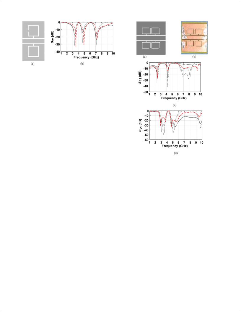
when two out of the four short circuits in Fig. 2(a) are moved 1 mm upward as shown in Fig. 8(a). The first resonator is presented by the λ/4 stub from the neck until the short circuit to the right while the second resonator is the series λ/4 stub from the neck until the short circuit to the left. There is a third rejection opportunity by the λ/2 U-shaped resonator. Since the transmission zeros are very close to each other, there might be a strong opportunity to obtain two rejected frequencies with a poor transmission band between them. In addition, there might be a slight coupling between the near and the rear horizontal slotlines. The constructing of the equivalent circuit model follows the same procedure previously discussed. The only difference is that the short circuits do not stop the propagation around the patch; therefore they are modeled as in Fig. 4(j). The effect of the parasitic loop is investigated by the removal of the loop which results in the filter configuration shown in Fig. 8(b). Figs. 9 and 10 show the measured and simulated frequency response for the basic cells in Fig. 8(a) and (b), respectively. The measured bandwidth for an insertion loss below −6 dB extends from 5.5 GHz to 9.5 GHz, which corresponds to 53% relative bandwidth. Once the parasitic loop is removed the response is almost unchanged except for a slight shift in the second transmission zero from 8.77 GHz to 9 GHz. This is explained by the elimination of the loading effect presented by the parasitic loop.
5) One Short Circuit Without Symmetry: The transmission line model for the asymmetric modified dumbbell in Fig. 11(a)
is simply a superposition of the modified dumbbell case (onehalf wavelength etched stub) in Fig. 1(a) and the case of the 1-D horizontal symmetry modified dumbbell with two short circuits (two λ/4 etched stubs) in Fig. 3(a). The frequency response is a bandreject filter with three independent transmission zeros measured at 3.4 GHz, 4.8 GHz, and 7.1 GHz. This response is attractive for bandstop applications where the frequencies to be rejected are neither even nor odd multiples of each other. The equivalent circuit model consists of the same model of the 1-D horizontal symmetry modified dumbbell with two short circuits for the upper resonator and the model of the modified dumbbell for the lower resonator. In addition, the model proposed in [13] is used for the transition from the coplanar waveguide to the slotline. This is to account for the excitation of the coplanar odd mode. The S21 response is shown in Fig. 11(b) where a discrepancy between the transmission line model and the measurements is seen above the third transmission zero measured at 7 GHz. This discrepancy is due to the capacitive effect added by the λ/2 etched resonator.
III. Applications
Once two or more basic cells are closely spaced, strong coupling occurs and the transmission zeros split. This technique has the advantage of improving the quality factor of the filter. The use of the transmission line models in the synthesis of such configurations saves the long time spent by the 3-D EM solvers for simulating structures involving closely coupled resonators.
ABDEL AZIZ et al.: COPLANAR WAVEGUIDE FILTERS BASED ON MULTIBEHAVIOR ETCHED-GROUND STUBS |
821 |
Fig. 11. Asymmetrical modified dumbbell with one short circuit.
(a) Schematic. (b) Experimental (solid line), transmission line model (gray line), and EM simulation (dashed line) S21 response.
A.Narrow Second-Order Bandpass Filter
1)Design Procedure: The 1-D symmetry modified dumbbell with two short circuits of Fig. 3(a) will serve as the fundamental building block for the second-order narrow bandpass filter around 4 GHz shown in Fig. 12(a). The two λ/4 etched stubs will correspond to 3 GHz and 5 GHz transmission zeros, therefore the dimensions of the patch and the rectangular hole have been slightly modified from those of the basic cells corresponding to Fig. 3(a). The modeling parameters have been readjusted yet the procedure is still the same.
2)Results: This prototype was previously proposed in [5] but the model was not considering the coupling between the adjacent slotlines nor the even/odd characteristic impedances in the coupling region between the two cells. Fig. 12 presents a comparison between the frequency response of the two closely coupled cells as per the transmission line model of [5] and the modified transmission line model presented herein with respect to the measured and the EM simulated response. The transmission line model previously presented in [5] did not take into account the coupling between the adjacent slotlines and considered only the even characteristic impedance in the coupling region between the two cells. Unlike the model of [5], the splitting in the transmission zeros is clearly seen with the modified model. This is an important figure as the larger is the splitting the higher is the coupling between the two cells. In addition, the newly proposed model gives a more accurate value for the insertion loss. Table I presents a quantitative comparison between the model of [5], the modified transmission line model and the EM solver results with respect to the measured results. In conclusion, the modified transmission line model shows more accuracy in terms of the transmission zeros and the insertion loss with respect to the EM solver, yet it shows a lower accuracy for the −3 dB bandwidth. Both the transmission line model and the EM solver show some deviations in the insertion loss and the return loss with respect
to the measured results from 6 GHz to 10 GHz. As one can see on the return loss curve shown in Fig. 12(c), spurious harmonics from the EM simulation are shifted from the ones obtained by the analytical model. This deviation might be attributed to various reasons. First one is the dispersive nature of the slotlines our model does not take into account. Moreover, high-dielectric loss in the FR4 substrate at 8 GHz impedes this resonance from occurring. Since the aim was
Fig. 12. Narrow second-order bandpass filter. (a) Schematic. (b) Fabricated structure. Experimental (solid line), transmission line model of [12] (gray double dashed line), modified transmission line (gray line), and EM simulation (dashed line). (c) Return loss. (d) Insertion loss.
to compare analytical together with numerical simulations, EM simulations does not deal with conductor loss which also explains the discrepancy between the measurements and the numerical results at high-frequencies. Finally, the remaining discrepancy at high-frequencies concerns radiations, hard to consider in analytical cases but obviously existing in practical cases as well as in numerical ones.
B.Low-Pass Filter With a Wide Bandstop
1)Design Procedure: All the modified dumbbell structures presented herein show a lowpass response for the band of frequencies below the lowest transmission zero. This is attributed to the inductive nature of the etched stubs below the resonance frequency [11]. Therefore, a lowpass filter with a wide bandstop response can be easily achieved by coupling two or more cells of identical or different topologies so as to broaden the rejection band. The limitation in such a procedure is the occupied area and the isolation provided by the resulting structure.
2)Configuration #1: The first topology proposes a 3 GHz lowpass filter. It consists of five cells as shown in Fig. 13(a) where the three middle cells are the λ/2 etched stub cells of Fig. 1(a), i.e., each cell introduces a transmission zero at 4.6 GHz. Each outer cell consists of two series connected λ/4

822 |
IEEE TRANSACTIONS ON COMPONENTS AND PACKAGING TECHNOLOGIES, VOL. 32, NO. 4, DECEMBER 2009 |
TABLE I
Quantitative Comparison Between the Transmission Line Model of [5], the Modified Transmission Line Model, and the EM Solver
Results, With Respect to the Measured Results
|
Meas. |
Model of [5] |
Modified Model |
EM Solver [6] |
|||
|
Abs. |
Abs. |
Rel. error |
Abs. |
Rel. error |
Abs. |
Rel. error |
Resonance frequencies fr (GHz) |
2.93 |
3.38 |
+0.15 |
3.03 |
+0.03 |
2.88 |
−0.02 |
|
3.62 |
3.38 |
−0.06 |
3.58 |
−0.01 |
3.73 |
+0.03 |
|
4.8 |
5.12 |
+0.06 |
4.62 |
−0.03 |
4.72 |
−0.02 |
|
5.4 |
5.12 |
−0.05 |
5.37 |
−0.005 |
5.67 |
+0.05 |
Insertion loss (dB) |
−2.27 |
−0.02 |
−0.99 |
−0.92 |
−0.59 |
−0.32 |
−0.86 |
−3 dB BW |
0.11 |
0.12 |
+0.07 |
0.07 |
−0.37 |
0.14 |
+0.24 |
Pole frequency (GHz) |
4.23 |
4.226 |
0 |
4.176 |
−0.01 |
4.27 |
+0.01 |
Fig. 13. Lowpass filter with a wide stopband (topology #1). (a) Schematic.
(b) Fabricated structure. Experimental (solid line), transmission line model (gray line), and EM simulation (dashed line). (c) Return loss. (d) Insertion loss.
Fig. 14. Lowpass filter with a wide stopband (topology #2). (a) Schematic.
(b) Fabricated structure. Experimental (solid line), transmission line model (gray line), and EM simulation (dashed line). (c) Return loss. (d) Insertion loss.
etched stubs as in Fig. 3(a) where the short circuits are readjusted so as to introduce two transmission zeros at 4.6 GHz and 4.8 GHz.
This configuration is typical for a multistage lowpass filter. The rejection band is broadened by the splitting of five transmission zeros around 4.8 GHz. It occupies a relatively large area of 48 mm × 30 mm, yet it provides a good selectivity. The attenuation is around −20 dB from 3 GHz to 6.5 GHz as shown in the frequency response in Fig. 13. The transmission line model proposed shows better resolution over the EM solver in terms of the cutoff frequency, but lower resolution in terms of the isolation level within the stopband.
3) Configuration #2: The second topology proposes another 3 GHz lowpass filter. It consists from left to right of the three cells of Figs. 3(a), 1(a), and 11(b) as shown in Fig. 14(a). The total area is 34 mm length × 30 mm width. Unlike the configuration #1, each cells contributes in the stopband with different values of transmission zeros. Fig. 14 presents the corresponding frequency response where the stopband extends from 2.6 GHz to 8.6 GHz. The left most cell defines the outer limits: 3.2 GHz and 7.6 GHz. These two transmission zeros are then splitted into four (3 GHz, 3.5 GHz, 7 GHz, and 8 GHz) thanks to the mutual coupling with the middle cell. The right most cell introduces another transmission zero in the middle of the stopband at 4.6 GHz. The middle cell slows down the

ABDEL AZIZ et al.: COPLANAR WAVEGUIDE FILTERS BASED ON MULTIBEHAVIOR ETCHED-GROUND STUBS |
823 |
signal and thus broadens the stopband. This topology offers fewer ripples in the passband when compared with topology #1. It shows 41% area reduction. This is at the expense of less isolation in the stopband. In addition, the use of a lower number of cells reduces the radiation, dielectric, and conductor losses which in turns, improves the insertion loss of the lowpass filter. Since the proposed model parameters are directly related to the physical dimensions and the topology of the structure it shows higher resolution in terms of the cutoff frequency and the position of the first transmission zero. It also shows better agreement with the measured return loss at 6.5 GHz. Yet it shows significant spikes around 9 GHz since the model parameters are extracted within the frequency band around the resonance frequency.
IV. Conclusion
The theory of operation of the modified dumbbell structures presented in [4] has been clarified. Such structures have been more clearly termed as etched-ground stubs structures. A design guideline is proposed using transmission line models. The proposed models have been verified for the different topologies. Three applications have been presented: a secondorder bandpass filter, and two topologies for a lowpass filter with a wide stopband. The proposed design procedure saves the long time consumed by the 3-D EM solvers when simulating closely coupled resonators. Moreover, the transmission line model shows in some aspects a better agreement with the measured results than the EM simulated results, especially in terms of the resonance frequencies. The EM solver would require more CPU time in order to achieve a higher resolution for applications like the closely coupled resonators presented herein.
Acknowledgment
The authors would like to thank N. Corrao, who is responsible for the platform microwaves, microwavephotonics, and electromagnetic characterization at the Institute of Microelectronics, Electromagnetism and PhotonicsLaboratory of High-frequencies and Characterization for performing the implementation and the measurements of the prototypes presented in Section III.
References
[1]D. Ahn, J.-S. Park, C.-S. Kim, J. Kim, Y. Qian, and T. Itoh, “A design of the low-pass filter using the novel microstrip defected ground structure,”
IEEE Trans. Microwave Theory Tech., vol. 49, no. 1, pp. 86–93, Jan. 2001.
[2]J.-S. Yoon, J.-G. Kim, J.-S. Park, C.-S. Park, J.-B. Lim, H.-G. Cho, and K.-Y. Kang, “A new DGS resonator and its application to bandpass filter design,” in Proc. IEEE Microw. Theory Tech. Soc. Int. Symp. Dig., vol. 3. TX, 2004, pp. 1605–1608.
[3]E. K. I. Hamad, A. M. E. Safwat, and A. S. Omar, “L-shaped defected ground structure for coplanar waveguide,” in Proc. IEEE Antennas Prop. Soc. Int. Symp. United Nations Security Council/Union Radio Scientifique Internationale Nat. Radio Sci. Meet., Washington D.C., Jul. 2005, pp. 663–666.
[4]A. M. E. Safwat, F. Podevin, P. Ferrari, and A. Vilcot, “Tunable bandstop defected ground structure resonator using reconfigurable dumbbell shaped coplanar waveguide,” IEEE Trans. Microwave Theory Tech., vol. 54, no. 9, pp. 3559–3564, Sep. 2006.
[5]M. A. Aziz, A. Safwat, F. Podevin, and A. Vilcot, “Narrow bandpass filter based on the modified DGS,” in Proc. 37th Eur. Microw. Conf. (EuMc), Munich, Germany, Oct. 2007, pp. 75–78.
[6]Microwave Studio User’s Guide, Wellesley, MA: Computer Simulations Technology (CST), 1998–2003.
[7]A. R. Djordjevic, M. B. Bazdar, T. K. Sarkar, and R. F. Harrington, “Linpar for windows: Matrix parameters for multiconductor transmission lines,” ver. 2. Software and User’s Manual, Norwood, MA: Artech House, 1999.
[8]Advanced Design System User’s Manual, Palo Alto, CA: Agilent Technologies, 1983–2006.
[9]J. Chramiec, “Reactances of slotline short and open circuits on alumina substrate,” IEEE Trans. Microwave Theory Tech., vol. 37, no. 10, pp. 1638–1641, Oct. 1989.
[10]J. Machac, J. Zehenter, W. Menzel, “Load impedances of complex slotline terminations,” in Proc. 25th Eur. Microw. Conf., vol. 2. Bologna, Italy, Oct. 1995, pp. 610–614.
[11]H.-M. Kim and B. Lee, “Bandgap and slow/fast-wave characteristics of defected ground structures (DGSs) including left-handed features,”
IEEE Trans. Microwave Theory Tech., vol. 54, no. 7, pp. 3113–3120, Jul. 2006.
[12]C. Quendo, E. Rius, and C. Person, “Narrow bandpass filters using dualbehavior resonators,” IEEE Trans. Microwave Theory Tech., vol. 51, no. 3, pp. 734–743, Mar. 2003.
[13]M. Ribo and L. Pradell, “Circuit model for a coplanar-slotline cross,”
IEEE Microw. Wirel. Comp. Lett., vol. 10, no. 12, pp. 511–513, Dec. 2000.
Marwa Abdel Aziz (S’00–M’04) was born in Cairo, Egypt, in September 1978. She received the B.S. and M.S. degrees in electrical engineering from Ain Shams University, Cairo, Egypt, in 2000 and 2004, respectively. She is currently working toward the Ph.D. degree in electrical engineering at the Institut de Microélectronique, Electromagnétisme et Photonique, Grenoble, France.
Her research interests include photonic bandgap and defected ground structure, slow-wave structures, and microwave planar antennas.
Amr M. E. Safwat (S’91–M’01) was born in Cairo, Egypt, in May 1970. He received the B.S. and M.S. degrees in electrical engineering from Ain Shams University, Cairo, Egypt, in 1993 and 1996, respectively, and the Ph.D. degree in electrical engineering from the University of Maryland, College Park, in 2001.
From August 2001 to August 2002, he was with Cascade Microtech, Inc., Beaverton, OR, where he co-developed the Infinity Probe. He has been an Assistant Professor in the Electronics and Communi-
cations Engineering Department of Ain Shams University since August 2002. He has held the position of Visiting Professor at Otto von Guericke University, Magdeburg, Germany (September–November 2004), Institut Polytechnique de Grenoble, Grenoble, France (September–November 2005) and at the Radio Laboratory and MilliLab, Helsinki University of Technology, Espoo, Finland (July 2006–June 2007). His research interests include microwave passive planar structures and microwave photonics.
Florence Podevin was born in France, in 1976. She received the Baccalaureat degree and the diploma from the Engineering School ECL in Lille, France, in 1993 and 1998, respectively, and the M.Sc and Ph.D. degrees, both in electronics and microelectronics engineering, from the Université des Sciences et Technologies de Lille (USTL) in France, in 1998 and 2001, respectively.
In 2001, she joined the Institut de Microélectronique, Electromagnétisme et Photonique (IMEP) in Grenoble, France, as an Assistant Professor, where
she is involved with the tunability of microwave devices, periodic structures filtering, and high frequency detectors.

824 |
IEEE TRANSACTIONS ON COMPONENTS AND PACKAGING TECHNOLOGIES, VOL. 32, NO. 4, DECEMBER 2009 |
Anne Vilcot received the M.S. degree in electronics from the Ecole Nationale Supérieure d’Electronique et de Radioélectricité de Grenoble, Grenoble Institute of Technology, Grenoble, France, in 1989, and the Ph.D. degree in microwaves from the Laboratory of Electromagnetism Microwaves and Optoelectronics (LEMO), Grenoble, France, in 1992.
In 1993, she joined LEMO as an Assistant Professor. She became a Full Professor in 2003. Since then, she has been involved in the optical control of microwave devices. She is currently a Full Professor
at the Institute of Microelectronics, Electromagnetics, and Photonics, Grenoble Institute of Technology. She is also the Head of Studies of the Phelma, School of Engineering in Physics, Electronics, and Materials, Grenoble. Her research interest includes microwaves photonics.