

J CIRCUIT SYST COMP Downloaded from www.worldscientific.com by KING`S COLLEGE LONDON MAUGHAN LIBRARY & INFORMATION SERVICES CENTRE (ISC) - JOURNAL SERVICES on 10/17/17. For personal use only.
Journal of Circuits, Systems, and Computers Vol. 27, No. 7 (2018) 1850100 (13 pages)
#c World Scienti¯c Publishing Company DOI: 10.1142/S0218126618501001
A Dual-Band Waveguide Bandpass Filter with Adjustable Transmission Zeros¤
Amit Bage† and Sushrut Das‡
Department of Electronics Engineering,
Indian Institute of Technology (Indian School of Mines),
Dhanbad 826004, Jharkhand, India
†bageism@gmail.com
‡sushrut_das@yahoo.com
Received 10 April 2017
Accepted 18 September 2017
Published 17 October 2017
This paper presents a planar insert-loaded compact, dual-pole, dual-band, waveguide bandpass ¯lter with adjustable multiple transmission zeros. Two identical inserts are placed on the transverse plane of a standard WR-90 waveguide at 8.41 mm distance to achieve the ¯lter characteristics. The insert consists of a stub-loaded C-shaped resonator and two asymmetric slot resonators. Two stub-loaded C-shaped resonators have been used to achieve dual-pole, dualband response whereas the asymmetric slot pairs have been used to introduce transmission zeros. The structure allows independent control of the center frequencies of the passbands and transmission zeros, which is useful to control the rejection level of out-of-band signals without disturbing the center frequency. Measured result shows a dual-pole, dual-band, bandpass response with center frequencies at 8.81 GHz and 10.9 GHz, the respective 3 dB bandwidths of 0.276 GHz and 0.398 GHz and transmission zeros at 8.02, 8.5, 9.46, 10.13, 11.53 and 12 GHz.
Keywords: Bandpass ¯lter; slot resonators; transmission zeros (TZs).
1. Introduction
Waveguide-based multiband ¯lters are widely used in high-power wireless systems due to their large power handling capability, low dielectric loss and rigid structures. However such ¯lters are bulky and heavier compared to planar ¯lters. Therefore, design of such ¯lters requires special attention to reduce their size and weight; in addition, to meet the primary goals like center frequencies, bandwidths and sharpness. The easiest way to design a dual-band bandpass ¯lter is to cascade a wideband bandpass ¯lter with a narrow stopband ¯lter.1 Following the technique Macchiarella
*This paper was recommended by Regional Editor Zoran Stamenkovic.
†Corresponding author.
1850100-1
J CIRCUIT SYST COMP Downloaded from www.worldscientific.com by KING`S COLLEGE LONDON MAUGHAN LIBRARY & INFORMATION SERVICES CENTRE (ISC) - JOURNAL SERVICES on 10/17/17. For personal use only.
A. Bage & S. Das
and Tamiazzo1 presented two dual-band bandpass ¯lters. The ¯rst has passbands of almost equal extension and the transmission zeros (TZs) are symmetrically placed in the stopband. The second has di®erent passbands but all the TZs should be at the same frequency. In 2008, Amari and Bekheit2 presented a dual-mode dual-band waveguide ¯lter. The passband is controlled by dedicated polarization in order to reduce the sensitivity of the ¯lter. The orientations of the input and output coupling apertures are adjusted in such a way that TZs are created between two passbands. In 2016, Jin3 presented the dual-band bandpass waveguide E-plane ¯lter using three pairs of resonators, the two pairs of resonators have been on the top of the dielectric substrate and one pair of resonators at the bottom of the dielectric substrate. In the same year, Stefanovski et al.4 presented a dual-band bandpass ¯lter based on H-plane metal insert with complementary split ring resonators (CSRRs). Two different lengths of the resonators are placed on the transverse plane of a standard WR90 rectangular waveguide. In 2017, Bage and Das5 presented the dual-pole tripleband bandpass ¯lter using seven concentric CSRR resonators. The out-of-band performances of these ¯lters are not good enough and they are easily a®ected by the interfering signals.
One of the ways to improve ¯lter stopband characteristics is to introduce multiple TZs above and below the passband. It is preferred that these TZs should be tunable so that better rejection of the out-of-band signals can be achieved. There are many techniques to control the TZs independently, some of them are use of cross-coupled resonator network,6 inline TM110-mode ¯lter with TE10-mode bypass coupling,7 source load coupling to introduce multiple coupling paths between the input output ports,8 dual-mode or multimode cavities,9 frequency-dependent techniques,10 fre- quency-selective surfaces11,12 etc. Although these ¯lters have improved stopband performance, they su®er from design complexity.
In this paper, a compact dual-pole dual-band waveguide bandpass ¯lter with multiple TZs has been presented using stub-loaded C-shaped resonator and asymmetrical slot resonators. The structure allows independent control of the center frequencies as well as the position of the TZs.
The organization of this paper is as follows. In Sec. 2, the design approach for the design of a dual-band bandpass ¯lter, but without transmission zeros, is presented. Section 3 presents the modi¯cations required in the resonator structure to introduce transmission zeros in the frequency response. The methodology behind the introduction of multiple transmission zeros has been described. It also establishes the independent control of the center frequency and transmission zeros. Finally, Sec. 4 describes the development of a dual-pole dual-band bandpass ¯lter with multiple transmission zeros and its frequency response. Comparative performances of the proposed dual-band waveguide ¯lter with few other similar bandpass ¯lters, reported in literatures, also have been presented. The paper is concluded in Sec. 5.
1850100-2

J CIRCUIT SYST COMP Downloaded from www.worldscientific.com by KING`S COLLEGE LONDON MAUGHAN LIBRARY & INFORMATION SERVICES CENTRE (ISC) - JOURNAL SERVICES on 10/17/17. For personal use only.
A Dual-Band Waveguide Bandpass Filter with Adjustable Transmission Zeros
2. Design Approach
The geometry of a C-shaped resonator is shown in Fig. 1 and its placement in a standard WR-90 rectangular waveguide is shown in Fig. 2. The C-shaped resonator has been chosen due to its simpler structure. The dimensions of such resonator are also easy to optimize for a given resonance frequency. In addition, such resonator allows use of stubs without increasing the footprint area. The proposed resonator has been designed on Roger RO4350 substrate (substrate thickness 0.762 mm, copper thickness 0.035 mm, relative permittivity 3.66 and loss tangent 0.004) due to its low loss characteristics. Equivalent circuit of the resonator can be represented as a parallel LC network, whose resonance frequency can be calculated using the relation4,5
!0 |
1 |
ð1Þ |
¼ p : |
||
|
LC |
|
For 500 characteristic impedance system, the lumped element values can be calculated using the relations provided in Ref. 5 after impedance scaling as
L |
i ¼ |
10B3dBi Z0ij S21ðj!0iÞ j |
; |
2 |
Þ |
|
2! 02i |
ð |
|||
Fig. 1. C-shaped resonator geometry.
Fig. 2. Integration of Fig. 1 into WR-90 rectangular waveguide.
1850100-3

J CIRCUIT SYST COMP Downloaded from www.worldscientific.com by KING`S COLLEGE LONDON MAUGHAN LIBRARY & INFORMATION SERVICES CENTRE (ISC) - JOURNAL SERVICES on 10/17/17. For personal use only.
A. Bage & S. Das
Fig. 3. Equivalent circuit of the proposed resonator with its lumped elemental values as L ¼ 0:29396 nH and C ¼ 0:70622 pF.
Ci ¼ |
2 |
; |
ð3Þ |
10B3dBi Z0ijS21ðj!0iÞj |
where jS21ðj!0iÞj and Z0i represent the magnitude of S21 and the characteristic impedance at the resonance frequency f0 and B3dBi represents the 3 dB bandwidth. Physically, the capacitance arises due to the gaps between the metallic parts and inductance arises due to the metallic parts of the structure. Therefore, the resonance frequency of the resonator can be controlled by varying ¯lter geometries.
The lumped equivalent circuit model of Fig. 2 is shown in Fig. 3. The simulated frequency responses of the structure in Fig. 2 (for L1 ¼ L2 ¼ 6 mm, G1 ¼ 0:7 mm, G2 ¼ 0:6 mm and W1 ¼ 0:3 mm) and its equivalent circuit are compared and shown in Fig. 4. The equivalent circuit parameters are obtained as L ¼ 0:294 nH and C ¼ 0:706 pF. The circuit parameters are extracted using the Eqs. (2) and (3). The ¯gure reveals that the structure resonates at 11.06 GHz with 3 dB bandwidth of 0.76 GHz.
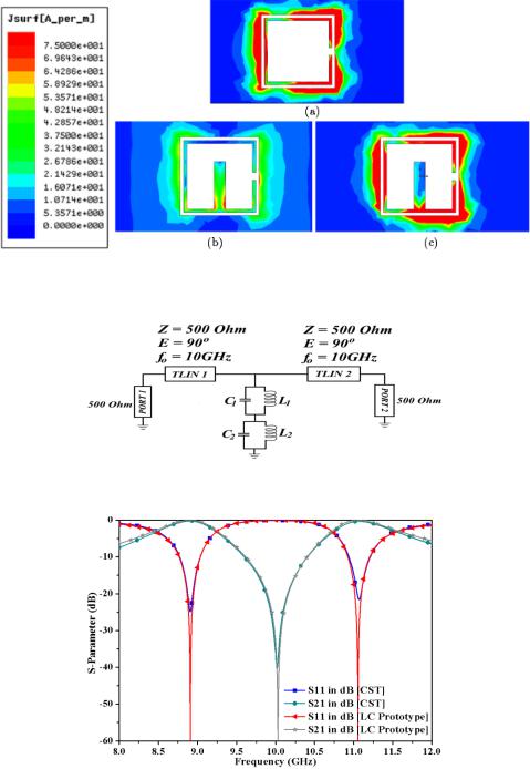
Figure 1 reveals that C-shaped resonator can provide a single passband. In order to achieve dual passband, the C-shaped resonator has been loaded with a stub, as shown in Fig. 5. To demonstrate the generation of singleand dual-band responses, the surface current distributions have been shown in Figs. 6(a)–6(c). Figure 6(a) reveals the maximum current distribution for a single-band resonance frequency at the C-shaped resonator. For dual bandpass responses, at the ¯rst resonance frequency of 8.91 GHz, the maximum current is distributed into the stub-loaded resonator, and the current distribution into the C-shaped resonator is very small. Due to these the stub is responsible for the generation of ¯rst band. At 11.06 GHz, the maximum current is distributed at the C-slot resonator and a negligible current at the loaded stub. So, the second band has been generated due to the C-shaped resonator. The above explanation reveals the generation of the dual passband responses. The equivalent circuit model for the dual passband responses has been shown in Fig. 7, and its elemental values can be extracted by using Eqs. (1) and (2). The extracted lumped elemental values are L1 ¼ 0:29396 nH, C1 ¼ 0:70622 pF, L2 ¼ 0:40498 nH and C2 ¼ 0:78759 pF.
1850100-4

J CIRCUIT SYST COMP Downloaded from www.worldscientific.com by KING`S COLLEGE LONDON MAUGHAN LIBRARY & INFORMATION SERVICES CENTRE (ISC) - JOURNAL SERVICES on 10/17/17. For personal use only.
A Dual-Band Waveguide Bandpass Filter with Adjustable Transmission Zeros
Fig. 4. Simulated frequency responses of Figs. 2 and 3.
Fig. 5. Proposed dual-band bandpass resonator structure (L1 ¼ L2 ¼ 6 mm, G1 ¼ 0:7 mm, G2 ¼ 0:3 mm, W1 ¼ 0:6 mm, W2 ¼ 1 mm and L3 ¼ 4:35 mm).
The frequency responses of Figs. 5 and 7 have been incorporated into Fig. 8, which reveals a single pole in the passband which is centered around 8.91 GHz and 11.06 GHz, respectively. In order to introduce the second pole another identical resonator has been placed at an optimized distance of 8.41 mm, as shown in Fig. 5. In the ¯gure, h indicates the thickness of the substrate, c indicates the thickness of the copper cladding and l represents the distance between the two identical inserts. The separation between the resonators is approximately quarter wavelength at the center of X-band and thus it forms an inverter.
The simulated frequency responses of the structures (Fig. 9) have been shown in Fig. 10. The frequency responses reveal dualband dual-pole response with center
1850100-5
J CIRCUIT SYST COMP Downloaded from www.worldscientific.com by KING`S COLLEGE LONDON MAUGHAN LIBRARY & INFORMATION SERVICES CENTRE (ISC) - JOURNAL SERVICES on 10/17/17. For personal use only.
A. Bage & S. Das
Fig. 6. Surface current distributions of single and dual passbands at (a) 11.06 GHz, (b) 8.91 GHz and (c) 11.06 GHz.
Fig. 7. Equivalent circuit model for dual passband.
Fig. 8. Simulated frequency responses of Figs. 5 and 7.
1850100-6