

диафрагмированные волноводные фильтры / 92dd89d4-03c2-4f24-a541-eb40bcab69c0
.pdfView metadata, citation and similar papers at core.ac.uk |
https://ntrs.nasa.gov/search.jsp?R=20160014507 2019-08-29T17:02:11+00:00Z |
|
brought to you by |
CORE |
|
|
provided by NASA Technical Reports Server |
|
4EPo2B-04 |
1 |
|
A Cryogenic Waveguide Mount for Microstrip Circuit and Material Characterization
Kongpop U-yen, Ari D. Brown, Member, IEEE, Samuel H. Moseley,
Omid Noroozian and Edward J. Wollack, Senior Member, IEEE
Abstract—A waveguide split-block fixture used in the characterization of thin-film superconducting planar circuitry at millimeter wavelengths is described in detail. The test fixture is realized from a pair of mode converters, which transition from rectangular-waveguide to on-chip microstrip-line signal propagation via a stepped ridge-guide impedance transformer. The observed performance of the W-band package at 4.2K has a maximum in-band transmission ripple of 2dB between 1.53 and 1.89 times the waveguide cutoff frequency. This metrology approach enables the characterization of superconducting microstrip test structures as a function temperature and frequency. The limitations of the method are discussed and representative data for superconducting Nb and NbTiN thin film microstrip resonators on single-crystal Si dielectric substrates are presented.
Index Terms—Material testing, millimeter wave devices, millimeter wave propagation, superconducting microwave devices.
I. INTRODUCTION
THE performance of cryogenic microwave circuits and systems have been significantly advanced through the use of low-loss dielectric and superconducting thin film materials.
In implementing the use of these materials the propagation properties must be known at the system’s operating frequency and temperature in order to reliably predict, design, and achieve the desired circuit response.
A variety of techniques have been used to study the properties of thin-films at cryogenic temperatures [1, 2]. However, many are best suited for exploring the DC and low frequency responses. At far infrared wavelengths, the material properties of homogenous superconducting thin-films have traditionally been explored via Fourier Transform Spectroscopy [3-5] and in more complex circuit settings when augmented with deembedding techniques [6]. Device characterization at microwave frequencies commonly relies on antenna-coupled
test structures combined with on-chip detection [2, 7-9].
Metrology based on these techniques generally simplifies the readout complexity; however increases the wafer fabrication overhead. Terahertz wafer probes are presently best suited for
This work was supported in part by the National Aeronautics and Space Administration under NNH12ZDA001N-APRA and Goddard Space Flight Center Internal Research and Development grants. (Corresponding author: Kongpop U-yen.)
Kongpop U-yen is with NASA Goddard Space Flight Center, Greenbelt, MD 20771 USA (e-mail: kongpop.u-yen-1@nasa.gov).
Ari D. Brown is with NASA Goddard Space Flight Center, Greenbelt, MD 20771 USA (e-mail: ari.d.brown@nasa.gov).
applications >10K due to the parasitic thermal loading and subsequent heating of the sample [10, 11].
In this paper superconducting films are characterized at millimeter wavelengths using a reusable waveguide mount configuration. The design described enables an appropriately prepared test device to be repeatedly positioned and precisely aligned with respect to metrology details incorporated in the waveguide fixture. The response of the sample can be calibrated and measured at cryogenic temperatures using standard vector network analyzer and mm-wave extension module waveguide interfaces. The design of the rectangular-waveguide to microstrip-line transition is discussed in Section II. The cryogenic waveguide test configuration used for validation of the packaging design concept is presented in Section III, followed by detailed measurement verification of test structures in Section IV. Finally, the concluding remarks and discussion are made in Section V.
II. WAVEGUIDE TO MICROSTRIP TRANSITION DESIGN
Waveguide is one of the most commonly used media in distributing single-mode mm-wave signals. Its low-loss properties, ease of fabrication, and rigid mechanical construction enables its use as a precision guiding media over wide range of operating conditions when used in conjunction with appropriate thermal isolation structures [12, 13]. To apply these measurement capabilities to the characterization of superconducting thin-film planar circuits, an appropriate modeconverter between waveguide and planar device structures is desired.
This transition can be performed using either non-contacting [14-16] or via physically contacting interfaces. In a noncontacting interface, a portion of the sample area is dedicated for use as a radiating element [17]. In addition, this technique requires relatively precise alignment between the coupling element and test sample, which can complicate fitting this structure within the waveguide cross-section and achievable resonance free bandwidth achievable. To enable efficient coupling many approaches resort to multiple metallization layers in the device structure [14], which increases the test sample’s overall fabrication complexity. On the other hand, an
Samuel H. Moseley is with NASA Goddard Space Flight Center, Greenbelt, MD 20771 USA (e-mail: samuel.h.moseley@nasa.gov).
Omid Noroozian is with University of Maryland, College Park, MD 20742 USA (e-mail: omid.noroozian@nasa.gov).
Edward J. Wollack is with NASA Goddard Space Flight Center, Greenbelt, MD 20771 USA (e-mail: edward.j.wollack@nasa.gov).

4EPo2B-04 |
2 |
Fig. 1. Cross-sectional view of the waveguide-to-microstrip transition employed for thin-film circuit and material characterization.
interface with physical film contact can be achieved through the use of a waveguide-planar transmission line mode converter [18]. This choice largely moves the complexity of the transition design to the waveguide housing and thus in principle reduces the sample fabrication overhead. Using a variation on this approach, a waveguide septum was introduced to transform the rectangular waveguide mode and reduce the guide height to the same thickness as the substrate.
A four-stage ridge-guide is used to convert from WR-10 waveguide to the microstrip line on a silicon substrate in use for test samples. The ridge-guide sections are implemented as a septum in an E-plane split-block housing and designed to provide efficient mode-conversion, a controlled impedance transformation, and physical contact to the microstrip line pads on the test structure. For a broadband spectral response, the microstrip line’s dielectric should be as thick as possible to maximize the microstrip pad contact area while maintaining single-mode transmission in the waveguide band. On the other hand, to limit the radiation loss from the microstrip structure, dielectric thickness should maintain small relative to the operating wavelength in order to minimize spurious electromagnetic coupling to the waveguide walls or septum.
The configuration’s electromagnetic performance was simulated using ANSYS HFSS (High Frequency Structural Simulator) finite-element electromagnetic simulation software.
An eigenmode analysis was used to evaluate the losses arising from various elements in the mount structure. The copper package walls limit the quality factor, Q = 2.1×10⁴, assuming a bulk resistivity of 1.68Ω-cm and a residual resistance ratio, RRR=10. For ohmic losses, to lowest order, Q scales as the square root of RRR for a normal metal. Similarly, the maximum quality factor achievable in the package, Qm, is limited to 7.04×10³ in the operating band between 80 and 100 GHz due to the proximity of the finite resistivity copper septum. The simulated S-parameter frequency response for the transition is shown in Fig. 2 and its optimized dimensions are provided in Fig.1.
The width of waveguide septum determines the contact area size as it is placed on top of the metal trace on the 50µm-thick
0 |
|
|
|
|
|
|
|
-10 |
|
|
|
|
|
|
|
dB-20 |
|
|
|
|
|
|
|
-30 |
|
|
|
|
|
|
S11 |
|
|
|
|
|
|
|
|
|
|
|
|
|
|
|
S21 |
-40 |
|
|
|
|
|
|
|
75 |
80 |
85 |
90 |
95 |
100 |
105 |
110 |
|
|
|
Frequency (GHz) |
|
|
|
|
Fig. 2. Simulated frequency response of the waveguide to 26-Ohm microstripline transitions in a back-to-back configuration.
single-crystal silicon substrate device layer. In this design the septum is 100µm wide and the 26Ω characteristic impedance microstrip line width is 150µm allowing the septum placement within a +/-25µm alignment tolerance. A pair of DC probes (Servometer part no. SK18648 from MW Industries, Inc.) are available in the fixture to provide DC bias or facilitate other onchip characterization needs.
III. HARDWARE IMPLEMENTATION AND MEASUREMENT
The E-plane split-block package was made from three copper pieces by direct CNC machining. See Fig. 3 for details. The waveguide septum was realized from a gold-plated 100-µm thick BeCu sheet fabricated using photo-chemical etching. Two of the copper blocks form the waveguide housing while the third is used to align and secure the microstrip test wafer in the fixture. The test device is pressed against the waveguide septum and with a physical contact force by a BeCu spring residing under the chip. Features machined into the split-block define the chip alignment with respect to the package housing. Alignment pins in the copper blocks are used to facilitate device assembly. In practice, the outer surfaces of the split-block housing are used as a reference to align the package elements with a precision machinist vice before tightening the housing fasteners.
To cryogenically test the package a section of thin-walled (thickness 250m) stainless steel waveguide was utilized as a
4EPo2B-04 |
3 |
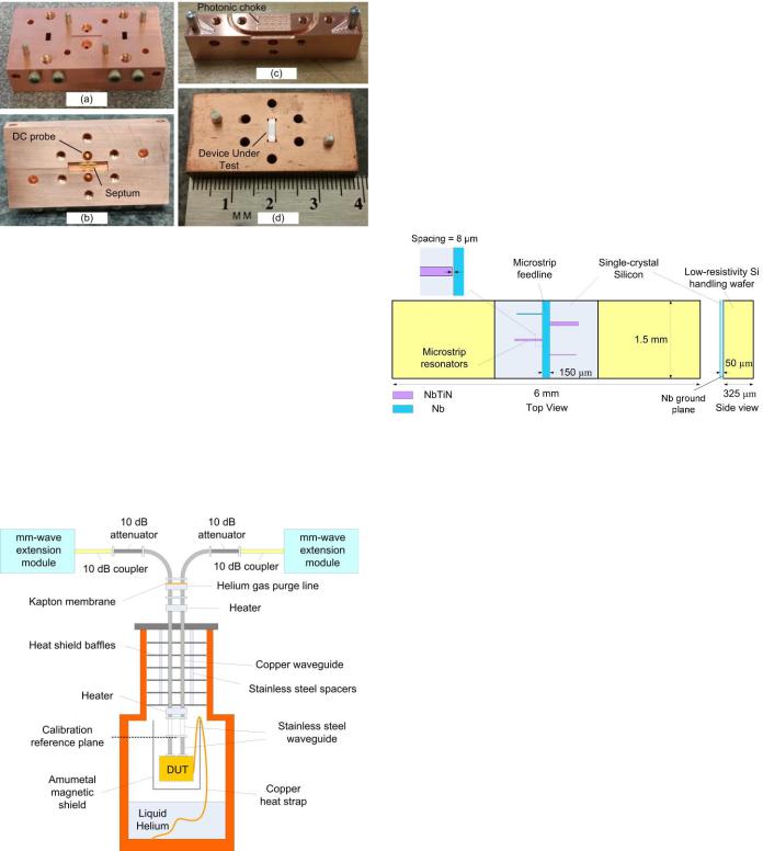
Fig. 3. Test fixture used for characterizing thin-film superconductor microstrip resonators (a) with gold-plated copper septum and DC probes when viewed from the bottom (b). The top-half contains waveguide channel and photonic choke (c). The bottom-half of the package contains chip alignment features (d).
thermal break as shown in Fig. 4. The room temperature ends of the waveguide are sealed by a 12m thick Kapton vacuum window and were connected to the WR-10 mm-wave extension modules and the PNA-X vector network analyzer. Helium gas is used to purge excess air from the package and the waveguide sections in cooling the device in the cryostat to 4.2K. A heater is used near the vacuum window interface to prevent cooling below the dew point and accumulation of condensates at this interface. Thermometry is provided by a calibrated (Lakeshore, DT-670) diode attached to the test fixture.
Fig. 4. Detail of the experimental setup used for superconducting circuit characterization at W-band frequencies that was connected to a PNA-X vector network analyzer.
The 10dB fixed attenuators are used to limit reflections and present an appropriate power level for the device under test (DUT). The test system was calibrated at room temperature using custom-made Thru-Reflect-Line (TRL) calibration
standards at the fixture’s input interface. The packaged device was enclosed in a magnetic shield to suppress interactions between the Earth’s magnetic field and the superconducting test device.
Test devices for cryogenic material characterization were fabricated, which contain three NbTiN and one Nb halfwavelength resonators coupled to a Nb microstrip feed line as shown in Fig. 5. The test chip ground plane is realized from 0.5m thick Nb. This configuration enables the test package transmission as well as loss to be evaluated in the superconducting film through quality factor measurement [1921].
Fig. 5. Device under test contained Nb and NbTiN microstrip resonators. The NbTiN resonator microstrip line widths are 80, 40, 20 µm and lengths are 550, 534, 510 µm, respectively. The Nb resonator is 20 µm wide and 510 µm long. The resonators are placed at 8 µm away from the feed line, respectively to define the microstrip resonator coupling.
The measurement results show relatively uniform transmission between 90 GHz and 110 GHz (e.g., see Fig. 6). The Nb resonator was designed to have the highest resonance frequency in the operating band. It was used to determine the dielectric loss of the substrate through the measurement of its quality factor and serves as a reference for the NbTiN resonators in the determination of the kinetic inductance. The kinetic inductance can be extracted by comparing the measured resonance frequency with that simulated using with single-sheet surface impedance model on the trace and ground plane as described in [20] and using SONNET or other electromagnetic simulation software. A kinetic inductance of ~0.81 pH/square for NbTiN and ~0.097 pH/square for Nb films respectively at 4.36K is found with this method. This is larger than the ~0.61 pH/square for NbTiN computed through the numerical integration of the Mattis-Bardeen integrals [21] adopting the measured sheet thickness of 150nm, critical temperature of 15K, and observed normal-state sheet resistivity of 79.4µΩ-cm.
The resonator parameters such as total quality factor (Qt), coupling quality factor (Qc), intrinsic quality factor (Qi), and center resonance frequency (f0) were extracted using a fit to the measured complex transmission S21. Fig. 7 shows the resulting model fit for one of the Nb resonators measured at 4.5 K. The model fit accounts for rotation effects due to impedance mismatch of the feedline on chip and the waveguide, using the circuit and technique described in [20, 22]. Using this method, Qi of 2,671 and Qc of 3,542, are extracted. This serves as an

4EPo2B-04 |
|
|
|
|
|
|
|
|
0 |
|
|
|
|
|
|
(dB) |
-5 |
|
|
|
|
|
|
|
|
|
|
|
|
|
|
Transmission |
-10 |
|
|
|
|
|
|
-15 |
|
|
|
|
4.36K |
|
|
|
|
|
|
|
|
300K |
|
|
-20 |
|
|
|
|
|
|
|
80 |
85 |
90 |
95 |
100 |
105 |
110 |
Frequency (GHz)
Fig. 6. Measured Nb microstrip line resonators transmission response at 300 K and at 4.36 K using waveguide-microstrip package. The data are uncorrected for the 33 mm length of WR10.0 stainless steel waveguide after the VNA calibration reference plane and the temperature change of the guide structures upon cooling from ambient (see Fig. 4).
Fig. 7. Complex scattering parameter amplitude, S21, (left) and power transmission (right) are measured and fit at a resonator physical temperature of 4.5K.
upper bound to the resonator’s internal resonator quality factor as the analysis does not formally correct for the losses arising from radiative coupling between the device and the package enclosure. A discussion of this and related considerations can be found in [23].
IV. CONCLUSION
A waveguide split-block fixture was designed and fabricated for thin-film circuit and material characterization at W-band frequencies. Although demonstrated in a wet cryogen dewar, the approach is more generally applicable in cryo-cooled systems with appropriately defined thermal isolation. Superconducting film phase velocity and dielectric loss measurements are demonstrated at millimeter wavelengths through the characterization of the transmission of halfwavelength niobium resonators in a reusable-mounting fixture.
ACKNOWLEDGMENT
Authors would like to acknowledge O. Rivera for providing CAD package drawing, K. Rostem for assisting with cryogenic measurements, and M. Berkeley for efforts in refining the cryostat and instrumentation used in this work.
REFERENCES
[1]C. Wilker, Z. Y. Shen, V. X. Nguyen and M. S. Brenner, "A sapphire resonator for microwave characterization of superconducting thin films," in IEEE Trans. Appl. Supercond., March 1993, vol. 3, no. 1, pp. 14571460.
4
[2]J. Gao, A. Vayonakis, O. Noroozian, J. Zmuidzinas, P.K. Day, H.G.
Leduc, “Measurement of loss in superconducting microstrip at millimeterwave frequencies”, 2009, Low Temperature Detectors LTD 13, AIP
Conference Proceedings, No.1185, pp. 164-167.
[3]K.E. Kornelsen, M. Dressel, J.E. Eldridge, M.J. Brett, K.L. Westra, “Farinfrared optical absorption and reflectivity of a superconducting NbN film”, 1991, Phys. Rev. B 44, 11882.
[4]V.B. Anzin, B.P. Gorshunov, G.V. Kozlov, A.A. Volkov, S.P. Lebedev,
I.V. Fedorov, “Measurement of Electrodynamic Parameters of
Superconducting Films in Far-Infrared and Submillimeter Frequency
Ranges”, 1993, Applied Superconductivity, Vol.1, No. 3-6, pp. 467-478.
[5]M. Šindler, R. Tesař, J. Koláček, L. Skrbek, and Z. Šimša, “Far-infrared transmission of a superconducting NbN film”, 2010, Phys. Rev. B 81,
184529.
[6]G. de Lange, J.J. Kuipers, T.M. Klapwijk, R.A. Panhuyzen, H. van de
Stadt, M.W.M. de Graauw, “Superconducting resonator circuits at frequencies above the gap frequency”, 1995, Journal of Applied Physics,
77, 1795-1804.
[7]T.M. Weller, L.P. Katehi, G.M. Rebeiz, “A 250-GHz Microshield Bandpass Filter”, 1995, IEEE Microwave and Guided Wave Letters, Vol.
5, No. 5., pp. 153-155.
[8]A. Vayonakis, C. Luo, H.G. Leduc, R. Schoelkopf, J. Zmuidzinas, “The millimeter-wave properties of superconducting microstrip lines” 2002,
Low Temperature Detectors LTD 9, AIP Conference Proceedings, No. 605, pp. 539-542.
[9]S. M. Jensen, R. B. Bass, A. W. Lichtenberger and A. M. Datesman, "A Simple GHz Resonator for Superconducting Materials Characterization," in IEEE Trans. on Applied Superconductivity, vol. 25, no. 3, pp. 1-4, June 2015.
[10]C. Zhang, M. Bauwens, N.S. Barker, R.M. Weikle, A.W. Lichtenberger, "A W-band balun integrated probe with common mode matching network," 2014, IEEE MTT-S International Microwave Symposium (IMS2014), Tampa, FL, 2014, pp. 1-4.
[11]‘THz probe arm’, Available: http://www.lakeshore.com/products/ Cryogenic-Probe-Stations/Pages/THz-Probe-Arm.aspx [Accessed: 30Aug- 2016]
[12]J. L. Hesler, A. R. Kerr, and N. Homer, "A boardband waveguide thermal isolator," 2003. Proc. Int. Symp. Space Terahertz Tech. vol. 14, pp. 148 154.
[13]E. J. Wollack, K. U-yen and D. T. Chuss, "Photonic choke-joints for dualpolarization waveguides," Microwave Symposium Digest (MTT), 2010 IEEE MTT-S International, Anaheim, CA, USA, 2010, pp. 177-180.
[14]S. Sun, Z. Wang, B. Yan and R. Xu, "Waveguide to microstrip transitions in W-band with LTCC technology," 2009 Asia Pacific Microwave Conference, Singapore, 2009, pp. 2515-2517.
[15]X. Huang and K. L. Wu, "A Broadband U-Slot Coupled Microstrip-to- Waveguide Transition," in IEEE Transactions on Microwave Theory and Techniques, vol. 60, no. 5, pp. 1210-1217, May 2012.
[16]J. H. C. Van Heuven, "A New Integrated Waveguide-Microstrip Transition," Microwave Conference, 1974. 4th European, Montreux, Switzerland, 1974, pp. 541-545.
[17]V. Hurm et al., "GaAs microstrip-to-waveguide transition operating in the WR-1.5 waveguide band (500–750 GHz)," 2012 Asia Pacific Microwave Conference Proceedings, Kaohsiung, 2012, pp. 145-147.
[18]Hui-Wen Yao, A. Abdelmonem, Ji-Fuh Liang and K. A. Zaki, "Analysis and design of microstrip-to-waveguide transitions," in IEEE Trans. on Microwave Theory and Techniques, vol. 42, no. 12, pp. 2371-2380, Dec 1994.
[19]G. Cataldo, E.J. Wollack, E.M. Barrentine, A.D. Brown, S.H. Moseley, K. U-Yen, “Analysis and calibration techniques for superconducting resonators“, 2015, Review of Scientific Instruments, 86, 013103.
[20]O. Noroozian, "Superconducting Microwave Resonator Arrays for Submillimeter/Far-Infrared Imaging", PhD dissertation, California Institute of Technology, 2012.
[21]T. R. Stevenson et al., "Superconducting Films for Absorber-Coupled MKID Detectors for Sub-Millimeter and Far-Infrared Astronomy," in IEEE Trans. on Applied Superconductivity, vol. 19, no. 3, pp. 561-564, June 2009.
[22]J. Gao, “The physics of superconducting microwave resonators,” Ph.D. dissertation, California Institute of Technology, 2008.
[23]E. J. Denlinger, "Radiation from Microstrip Resonators (Correspondence)," in IEEE Transactions on Microwave Theory and Techniques, vol. 17, no. 4, pp. 235-236, April 1969.